EP0442637B1 - Montage de circuit pour lier un amplificateur haute fréquence et un filtre de tension d'alimentation - Google Patents
Montage de circuit pour lier un amplificateur haute fréquence et un filtre de tension d'alimentation Download PDFInfo
- Publication number
- EP0442637B1 EP0442637B1 EP91300811A EP91300811A EP0442637B1 EP 0442637 B1 EP0442637 B1 EP 0442637B1 EP 91300811 A EP91300811 A EP 91300811A EP 91300811 A EP91300811 A EP 91300811A EP 0442637 B1 EP0442637 B1 EP 0442637B1
- Authority
- EP
- European Patent Office
- Prior art keywords
- supply voltage
- circuit
- transistor
- emitter
- circuit arrangement
- Prior art date
- Legal status (The legal status is an assumption and is not a legal conclusion. Google has not performed a legal analysis and makes no representation as to the accuracy of the status listed.)
- Expired - Lifetime
Links
- 238000001914 filtration Methods 0.000 claims abstract description 15
- 239000003990 capacitor Substances 0.000 claims abstract description 11
- 230000003321 amplification Effects 0.000 description 3
- 238000003199 nucleic acid amplification method Methods 0.000 description 3
- 238000000926 separation method Methods 0.000 description 3
- 238000004088 simulation Methods 0.000 description 3
- 230000001419 dependent effect Effects 0.000 description 2
- 230000000694 effects Effects 0.000 description 2
- 230000002238 attenuated effect Effects 0.000 description 1
- 238000010276 construction Methods 0.000 description 1
- 230000000087 stabilizing effect Effects 0.000 description 1
Images

Classifications
-
- H—ELECTRICITY
- H03—ELECTRONIC CIRCUITRY
- H03F—AMPLIFIERS
- H03F3/00—Amplifiers with only discharge tubes or only semiconductor devices as amplifying elements
- H03F3/189—High-frequency amplifiers, e.g. radio frequency amplifiers
- H03F3/19—High-frequency amplifiers, e.g. radio frequency amplifiers with semiconductor devices only
Definitions
- the invention relates to a circuit in which the RF amplifier circuit also serves as a filter for the supply voltage produced from the supply voltage of the amplifier.
- a high frequency amplifier primarily a radio frequency amplifier
- a radio frequency amplifier has been implemented using a common emitter transistor i.e. the radio frequency signal to be amplified is applied to the transistor base and the amplified output signal is obtained from the collector circuit.
- the emitter of the transistor has in general been connected directly to the ground of the circuit.
- the operating point of the transistor is set from the supply voltage using resistors, and the DC separation of the input and the output is performed by means of capacitors.
- the collector current is determined with base current, which in turn is determined by the resistance division which sets the operating point.
- the temperature compensation of the bias voltage of the transistor is made, for instance, by using a diode or resistive counteraction obtained through the collector line. If the emitter has been connected to the ground of the circuit through a resistor and the emitter voltage is high, the junction voltage of the base emitter will not essentially change the collector current, whereas, on the other hand, power losses take place in the resistor connected to the emitter, through which resistor the emitter current approaching the magnitude of collector current runs.
- the filtering of the supply voltage may be arranged in a number of ways as is known in the art.
- One of the basic ways is to use a simple RC filter.
- a high ohm resistor and a high capacitance capacitor should be used.
- a drawback is the great voltage loss produced by the loading current passing through the resistor and also the power loss produced herewith.
- a very small resistor cannot be used because the filtering effect will be reduced.
- a more profitable way is to use an emitter follower circuit in which the supply voltage to be filtered is applied to the collector of the transistor the base of which has through a resistor been connected to the supply voltage to be filtered, and to the ground through a capacitor. The filtered supply voltage is received from the transistor emitter.
- the main current travels through the collector, and the base current, that is, the current passing through the resistor, has been reduced to a ⁇ (beta) part, compared with the current passing through the simple RC filter whereby a high RC input can be used.
- the present invention introduces a circuit arrangement with which the shortcomings of separate amplifier and filter circuits can be eliminated and with which the current passing through the amplifier transistor may be used for two purposes: first, in conjunction with amplifying the input signal of the amplifier, and second, as the current for the supply voltage to be produced.
- German Patent Application DE-A-27 12 680 discloses a multi-stage transistor amplifier having an ac voltage supply, which has at least two amplification stages coupled together. The sum of the currents of the coupled together-stages is used as the supply for a further amplification stage.
- European Patent Application EP-A-O 160 223 discloses a high voltage, high frequency amplifier employing transistors.
- the amplifier provides parallel ac signal amplification paths through each transistor and a single dc power path through the transistor in series.
- a circuit arrangement for combining a high frequency amplifier circuit, supplied by a first supply voltage input and including a common emitter transistor with ancillary components, and a filter circuit for a second supply voltage produced from the first supply voltage characterised in that
- the basic circuit of the invention comprises a common emitter amplifier including a transistor with ancillary components.
- Said amplifier circuit acts as a filter for the supply voltage which is taken from the emitter of the transistor.
- the transistor acts thus in the manner of filter circuits known in the art in the form of emitter follower in the filter in addition to RF amplifier activity. With said circuit, two separate circuits have been contacted into one circuit provided with two operations.
- FIG. 1 presents a circuit arrangement of the invention.
- the RF amplifier comprises a transistor Q1, resistors R1, R2 and R3, capacitors C1, C2, C3, C4, C5, and a coil L1.
- the filtering circuit of the supply voltage V cc out comprises, excluding the DC separation capacitors C3 and C4 of the RF signals, all components of the RF amplifier circuit, and in addition, the resistor R4 and the capacitor C6.
- the amplifier part operates as follows: the voltage dividing resistors R1, R2 and R3 determine the bias voltage of the base of the transistor Q1, and the collector current is determined by the load connected to the voltage V cc out. Said loading current is expected to be as steady as possible since when approaching the collector current of the transistor, its magnitude affects the gain of the transistor.
- An appropriate loading may be, for instance, another amplifier, an IC circuit, or equivalent.
- the emitter capacitor C5 grounds the emitter at the operational range of RF amplifier, and the coil L1 provides the impedance matching of the output RFout for the present frequency.
- the capacitors C3 and C4 are provided for the DC separation of the RF signals, and the C1 is used as a filter for stabilizing the bias voltage.
- the present circuit operates in the manner of a common emitter amplifier.
- the filter circuit of the supply voltage V cc out As regards the voltage V cc out, the transistor Q1 serves as the emitter follower, and its bias-voltage is determined as already described above, at the resistor division R1, R2, R3. The voltage obtained from the emitter of the current buffer Q1 is conducted through the resistor R4 to be the load voltage V cc out. Said voltage is naturally expected to be so high that it suffices for the circuit serving as the load.
- the filtering of the supply voltage V cc out is performed in circuits R1-C1 and C5-R4-C6.
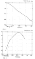
- Fig. 2 shows a simulation of the attenuation of a signal between the supply voltages V cc and V cc out.
- the frequency is 10 Hz to 1G Hz and on the vertical axis, the attenuation is 0 to 200 dB.
- a 1 kHz signal fed to V cc when viewed from the V cc out output, attenuated 30 dB, and a 100 kHz signal over 80 dB.
- this attenuation is sufficient.
- the attenuation is, of course, dependent on the component values used, but this simulation informs, however, of the order of magnitude of attenuation.
- Fig. 3 In the simulation of Fig. 3 is presented a typical gain curve between RFin and RFout. In the range 150 MHz to 1 GHz, the gain is over 10 dB. Even this value is actually dependent on the component values used.
- the arrangement of the invention in which the filtering of the voltage of the amplifier connection produced from the supply voltage and the amplifier itself constitute a combined circuit saves both components and power in comparison with the separate arrangements known.
- the supply voltage can be utilized efficiently with the described double connection.
- the practical circuit realization can be implemented in a plurality of ways.
- the input matching, the output matching and the biasing of the. transistor are implemented to meet the requirements in each instance.
- the filter section may also comprise a plurality of filtering blocks to be in conformance with the requisite filtering requirements. All of this is obvious to a person skilled in the art and feasible to be implemented within the scope of protection of the claims.
Landscapes
- Engineering & Computer Science (AREA)
- Power Engineering (AREA)
- Amplifiers (AREA)
- Hall/Mr Elements (AREA)
- Optical Recording Or Reproduction (AREA)
- Networks Using Active Elements (AREA)
Claims (6)
- Agencement de circuit destiné à combiner un circuit d'amplificateur à haute fréquence, alimenté par une première entrée de tension d'alimentation (VCC) et comprenant un transistor à montage à émetteur commun (Q1) et des composants accessoires, et un circuit de filtrage pour une seconde tension d'alimentation (VCC de sortie) produite à partir de la première tension d'alimentation (VCC), caractérisé en ce quele filtre est un filtre actif obtenu en disposant des composants de filtrage (R1, C1) au niveau du cheminement de la circulation du courant dudit transistor à montage à émetteur commun (Q1),un autre composant (R2) est prévu entre les composants de filtrage (R1, C1) et la base dudit transistor à montage à émetteur commun (Q1),la seconde tension d'alimentation (VCC de sortie) est sortie depuis l'émetteur dudit transistor (Q1),l'émetteur dudit transistor (Q1) est relié à la masse de l'agencement de circuit par l'intermédiaire d'un premier condensateur (C5), etledit transistor (Q1) sert de montage émetteur-suiveur dans ledit filtre actif.
- Agencement de circuit selon la revendication 1, comprenant en outre un ou plusieurs étages de filtres (R4, C6) reliés après le circuit d'amplificateur à haute fréquence, afin de filtrer davantage la seconde tension d'alimentation (VCC de sortie).
- Agencement de circuit selon la revendication 1, caractérisé en ce que ledit autre composant est un élément résistif (R2).
- Agencement de circuit selon l'une quelconque des revendications 1 à 3, dans lequel la seconde tension d'alimentation (VCC de sortie) est destinée à appliquer une tension à une charge.
- Agencement de circuit selon la revendication 4, dans lequel la charge comprend un circuit intégré.
- agencement de circuit selon la revendication 4 ou 5, dans lequel la charge comprend un autre amplificateur.
Applications Claiming Priority (2)
| Application Number | Priority Date | Filing Date | Title |
|---|---|---|---|
| FI900803A FI87027C (fi) | 1990-02-16 | 1990-02-16 | Kopplingsanordning foer foerening av rf-foerstaerkare och driftspaenningsfilter |
| FI900803 | 1990-02-16 |
Publications (3)
| Publication Number | Publication Date |
|---|---|
| EP0442637A2 EP0442637A2 (fr) | 1991-08-21 |
| EP0442637A3 EP0442637A3 (en) | 1992-01-29 |
| EP0442637B1 true EP0442637B1 (fr) | 1998-04-22 |
Family
ID=8529899
Family Applications (1)
| Application Number | Title | Priority Date | Filing Date |
|---|---|---|---|
| EP91300811A Expired - Lifetime EP0442637B1 (fr) | 1990-02-16 | 1991-02-01 | Montage de circuit pour lier un amplificateur haute fréquence et un filtre de tension d'alimentation |
Country Status (4)
| Country | Link |
|---|---|
| EP (1) | EP0442637B1 (fr) |
| AT (1) | ATE165481T1 (fr) |
| DE (1) | DE69129278T2 (fr) |
| FI (1) | FI87027C (fr) |
Families Citing this family (5)
| Publication number | Priority date | Publication date | Assignee | Title |
|---|---|---|---|---|
| GB2268348B (en) * | 1992-06-30 | 1996-01-03 | Texas Instruments Ltd | Noise reduction circuit |
| US5809410A (en) * | 1993-07-12 | 1998-09-15 | Harris Corporation | Low voltage RF amplifier and mixed with single bias block and method |
| US5424686A (en) * | 1994-04-20 | 1995-06-13 | Philips Electronics North America Corporation | Negative-resistance-compensated microwave buffer |
| US5498997A (en) * | 1994-12-23 | 1996-03-12 | Schiebold; Cristopher F. | Transformerless audio amplifier |
| US7015755B2 (en) * | 2001-08-31 | 2006-03-21 | Nokia Corporation | Stacked modulator and automatic gain control amplifier |
Citations (1)
| Publication number | Priority date | Publication date | Assignee | Title |
|---|---|---|---|---|
| EP0160223A2 (fr) * | 1984-04-27 | 1985-11-06 | GTE Laboratories Incorporated | Amplificateur haute fréquence |
Family Cites Families (3)
| Publication number | Priority date | Publication date | Assignee | Title |
|---|---|---|---|---|
| US3422365A (en) * | 1965-05-28 | 1969-01-14 | Wilcox Electric Co Inc | Stabilized transistor amplifier |
| US3671884A (en) * | 1970-09-29 | 1972-06-20 | Gen Electric | Improved amplifying circuit |
| DE2712680C2 (de) * | 1977-03-23 | 1982-10-21 | Robert Bosch Gmbh, 7000 Stuttgart | Mehrstufiger Transistorverstärker für Wechselspannungen |
-
1990
- 1990-02-16 FI FI900803A patent/FI87027C/fi not_active IP Right Cessation
-
1991
- 1991-02-01 AT AT91300811T patent/ATE165481T1/de active
- 1991-02-01 EP EP91300811A patent/EP0442637B1/fr not_active Expired - Lifetime
- 1991-02-01 DE DE69129278T patent/DE69129278T2/de not_active Expired - Fee Related
Patent Citations (1)
| Publication number | Priority date | Publication date | Assignee | Title |
|---|---|---|---|---|
| EP0160223A2 (fr) * | 1984-04-27 | 1985-11-06 | GTE Laboratories Incorporated | Amplificateur haute fréquence |
Also Published As
| Publication number | Publication date |
|---|---|
| FI87027C (fi) | 1992-11-10 |
| DE69129278T2 (de) | 1998-11-12 |
| FI900803A0 (fi) | 1990-02-16 |
| FI87027B (fi) | 1992-07-31 |
| EP0442637A3 (en) | 1992-01-29 |
| DE69129278D1 (de) | 1998-05-28 |
| ATE165481T1 (de) | 1998-05-15 |
| FI900803L (fi) | 1991-08-17 |
| EP0442637A2 (fr) | 1991-08-21 |
Similar Documents
| Publication | Publication Date | Title |
|---|---|---|
| US5241284A (en) | Circuit arrangement for connecting RF amplifier and supply voltage filter | |
| US7535289B2 (en) | Integrated RC filter | |
| CA1153076A (fr) | Amplificateur differentiel couple par resonateur | |
| US4713628A (en) | Compensation and biasing of wideband amplifiers | |
| EP0938776A1 (fr) | Etage d'amplificateur cascode replie | |
| US5774019A (en) | Low distortion differential amplifier circuit | |
| US5057788A (en) | 2-stage differential amplifier connected in cascade | |
| KR100830812B1 (ko) | 고주파 증폭기 회로 | |
| US5945880A (en) | Low noise amplifier | |
| US5923216A (en) | Frequency selective amplifier circuit | |
| GB2406728A (en) | A current mirror bias sensing circuit for a low-noise low-voltage RF amplifier | |
| US5424686A (en) | Negative-resistance-compensated microwave buffer | |
| EP0442637A2 (fr) | Montage de circuit pour lier un amplificateur haute fréquence et un filtre de tension d'alimentation | |
| US4460876A (en) | Low consumption, wide-band linear amplifier operating in sliding class A | |
| US4540950A (en) | Wideband linear amplifier | |
| US3631356A (en) | Controllable amplifier stage | |
| RU2053592C1 (ru) | Усилитель | |
| US5760651A (en) | Inductorless voltage biasing circuit for and Ac-coupled amplifier | |
| CA1121869A (fr) | Amplificateurs de puissance | |
| US4453135A (en) | Amplifier circuit arrangement having two amplifiers with respectively different electrical properties | |
| US5909147A (en) | Amplifier having DC coupled gain stages | |
| US5019788A (en) | Amplifier with wide dynamic range | |
| EP0765028A2 (fr) | Dispositifs amplificateurs | |
| US5903190A (en) | Amplifier feedforward arrangement and method for enhanced frequency response | |
| JPH0572129B2 (fr) |
Legal Events
| Date | Code | Title | Description |
|---|---|---|---|
| PUAI | Public reference made under article 153(3) epc to a published international application that has entered the european phase |
Free format text: ORIGINAL CODE: 0009012 |
|
| AK | Designated contracting states |
Kind code of ref document: A2 Designated state(s): AT BE CH DE DK ES FR GB GR IT LI LU NL SE |
|
| PUAL | Search report despatched |
Free format text: ORIGINAL CODE: 0009013 |
|
| AK | Designated contracting states |
Kind code of ref document: A3 Designated state(s): AT BE CH DE DK ES FR GB GR IT LI LU NL SE |
|
| 17P | Request for examination filed |
Effective date: 19920701 |
|
| 17Q | First examination report despatched |
Effective date: 19940906 |
|
| GRAG | Despatch of communication of intention to grant |
Free format text: ORIGINAL CODE: EPIDOS AGRA |
|
| GRAG | Despatch of communication of intention to grant |
Free format text: ORIGINAL CODE: EPIDOS AGRA |
|
| GRAH | Despatch of communication of intention to grant a patent |
Free format text: ORIGINAL CODE: EPIDOS IGRA |
|
| GRAH | Despatch of communication of intention to grant a patent |
Free format text: ORIGINAL CODE: EPIDOS IGRA |
|
| GRAH | Despatch of communication of intention to grant a patent |
Free format text: ORIGINAL CODE: EPIDOS IGRA |
|
| GRAA | (expected) grant |
Free format text: ORIGINAL CODE: 0009210 |
|
| AK | Designated contracting states |
Kind code of ref document: B1 Designated state(s): AT BE CH DE DK ES FR GB GR IT LI LU NL SE |
|
| PG25 | Lapsed in a contracting state [announced via postgrant information from national office to epo] |
Ref country code: IT Free format text: LAPSE BECAUSE OF FAILURE TO SUBMIT A TRANSLATION OF THE DESCRIPTION OR TO PAY THE FEE WITHIN THE PRE;WARNING: LAPSES OF ITALIAN PATENTS WITH EFFECTIVE DATE BEFORE 2007 MAY HAVE OCCURRED AT ANY TIME BEFORE 2007. THE CORRECT EFFECTIVE DATE MAY BE DIFFERENT FROM THE ONE RECORDED.SCRIBED TIME-LIMIT Effective date: 19980422 Ref country code: CH Free format text: LAPSE BECAUSE OF FAILURE TO SUBMIT A TRANSLATION OF THE DESCRIPTION OR TO PAY THE FEE WITHIN THE PRESCRIBED TIME-LIMIT Effective date: 19980422 Ref country code: AT Free format text: LAPSE BECAUSE OF FAILURE TO SUBMIT A TRANSLATION OF THE DESCRIPTION OR TO PAY THE FEE WITHIN THE PRESCRIBED TIME-LIMIT Effective date: 19980422 Ref country code: ES Free format text: THE PATENT HAS BEEN ANNULLED BY A DECISION OF A NATIONAL AUTHORITY Effective date: 19980422 Ref country code: NL Free format text: LAPSE BECAUSE OF FAILURE TO SUBMIT A TRANSLATION OF THE DESCRIPTION OR TO PAY THE FEE WITHIN THE PRESCRIBED TIME-LIMIT Effective date: 19980422 Ref country code: GR Free format text: LAPSE BECAUSE OF NON-PAYMENT OF DUE FEES Effective date: 19980422 Ref country code: BE Free format text: LAPSE BECAUSE OF FAILURE TO SUBMIT A TRANSLATION OF THE DESCRIPTION OR TO PAY THE FEE WITHIN THE PRESCRIBED TIME-LIMIT Effective date: 19980422 Ref country code: LI Free format text: LAPSE BECAUSE OF FAILURE TO SUBMIT A TRANSLATION OF THE DESCRIPTION OR TO PAY THE FEE WITHIN THE PRESCRIBED TIME-LIMIT Effective date: 19980422 |
|
| REF | Corresponds to: |
Ref document number: 165481 Country of ref document: AT Date of ref document: 19980515 Kind code of ref document: T |
|
| REG | Reference to a national code |
Ref country code: CH Ref legal event code: EP |
|
| REF | Corresponds to: |
Ref document number: 69129278 Country of ref document: DE Date of ref document: 19980528 |
|
| ET | Fr: translation filed | ||
| PG25 | Lapsed in a contracting state [announced via postgrant information from national office to epo] |
Ref country code: DK Free format text: LAPSE BECAUSE OF FAILURE TO SUBMIT A TRANSLATION OF THE DESCRIPTION OR TO PAY THE FEE WITHIN THE PRESCRIBED TIME-LIMIT Effective date: 19980722 |
|
| NLV1 | Nl: lapsed or annulled due to failure to fulfill the requirements of art. 29p and 29m of the patents act | ||
| REG | Reference to a national code |
Ref country code: CH Ref legal event code: PL |
|
| PG25 | Lapsed in a contracting state [announced via postgrant information from national office to epo] |
Ref country code: LU Free format text: LAPSE BECAUSE OF NON-PAYMENT OF DUE FEES Effective date: 19990201 |
|
| PLBE | No opposition filed within time limit |
Free format text: ORIGINAL CODE: 0009261 |
|
| STAA | Information on the status of an ep patent application or granted ep patent |
Free format text: STATUS: NO OPPOSITION FILED WITHIN TIME LIMIT |
|
| 26N | No opposition filed | ||
| REG | Reference to a national code |
Ref country code: GB Ref legal event code: IF02 |
|
| PGFP | Annual fee paid to national office [announced via postgrant information from national office to epo] |
Ref country code: GB Payment date: 20020130 Year of fee payment: 12 |
|
| PGFP | Annual fee paid to national office [announced via postgrant information from national office to epo] |
Ref country code: SE Payment date: 20020206 Year of fee payment: 12 |
|
| PGFP | Annual fee paid to national office [announced via postgrant information from national office to epo] |
Ref country code: FR Payment date: 20020212 Year of fee payment: 12 |
|
| PGFP | Annual fee paid to national office [announced via postgrant information from national office to epo] |
Ref country code: DE Payment date: 20020227 Year of fee payment: 12 |
|
| REG | Reference to a national code |
Ref country code: GB Ref legal event code: 732E |
|
| PG25 | Lapsed in a contracting state [announced via postgrant information from national office to epo] |
Ref country code: GB Free format text: LAPSE BECAUSE OF NON-PAYMENT OF DUE FEES Effective date: 20030201 |
|
| PG25 | Lapsed in a contracting state [announced via postgrant information from national office to epo] |
Ref country code: SE Free format text: LAPSE BECAUSE OF NON-PAYMENT OF DUE FEES Effective date: 20030202 |
|
| PG25 | Lapsed in a contracting state [announced via postgrant information from national office to epo] |
Ref country code: DE Free format text: LAPSE BECAUSE OF NON-PAYMENT OF DUE FEES Effective date: 20030902 |
|
| GBPC | Gb: european patent ceased through non-payment of renewal fee | ||
| EUG | Se: european patent has lapsed | ||
| PG25 | Lapsed in a contracting state [announced via postgrant information from national office to epo] |
Ref country code: FR Free format text: LAPSE BECAUSE OF NON-PAYMENT OF DUE FEES Effective date: 20031031 |
|
| REG | Reference to a national code |
Ref country code: FR Ref legal event code: ST |