EP0443154A2 - Appareil et méthode pour le traitement de surface de dispositifs microélectroniques - Google Patents
Appareil et méthode pour le traitement de surface de dispositifs microélectroniques Download PDFInfo
- Publication number
- EP0443154A2 EP0443154A2 EP90124468A EP90124468A EP0443154A2 EP 0443154 A2 EP0443154 A2 EP 0443154A2 EP 90124468 A EP90124468 A EP 90124468A EP 90124468 A EP90124468 A EP 90124468A EP 0443154 A2 EP0443154 A2 EP 0443154A2
- Authority
- EP
- European Patent Office
- Prior art keywords
- specimen
- surface treatment
- plasma
- ion beam
- etching
- Prior art date
- Legal status (The legal status is an assumption and is not a legal conclusion. Google has not performed a legal analysis and makes no representation as to the accuracy of the status listed.)
- Withdrawn
Links
Images




Classifications
-
- H—ELECTRICITY
- H01—ELECTRIC ELEMENTS
- H01J—ELECTRIC DISCHARGE TUBES OR DISCHARGE LAMPS
- H01J37/00—Discharge tubes with provision for introducing objects or material to be exposed to the discharge, e.g. for the purpose of examination or processing thereof
- H01J37/32—Gas-filled discharge tubes
- H01J37/32009—Arrangements for generation of plasma specially adapted for examination or treatment of objects, e.g. plasma sources
- H01J37/32357—Generation remote from the workpiece, e.g. down-stream
Definitions
- the present invention relates to an apparatus for and a method of surface treatment for carrying out dry etching, surface cleaning, thin film deposition and the like, and more particularly to an apparatus for and a method of surface treatment suitable for pattern delineation of microelectronic devices such as semiconductor integrated circuits.
- the dry etching technique is an indispensable technique for delineating very fine patterns of semiconductor integrated circuits in that pattern delineation on thin film materials can be made without pattern width shift from the mask width by making the most of directional movement of ions from plasma.
- Degradation of an insulating film by means of a plasma process as described above is generated because a large quantity of charged particles such as ions and electrons are incident on a specimen from plasma.
- the present inventor et al. have developed a technique of carrying out etching with a neutral beam without having charged particles be incident on a specimen surface by an apparatus and a method disclosed in JP-A-61-248428 and JP-A-62-259443.
- an ion beam extracted from plasma by accelerating to desired kinetic energy e.g., several hundred eV
- desired kinetic energy e.g., several hundred eV
- a part of the ion beam is converted into a neutral beam by charge exchange reactions with atoms and molecules in the gas
- residual ions are repelled to proceed by means of appropriate electric field or magnetic field which is applied in front of the specimen, and only the neutral beam is radiated onto the specimen.
- a gas containing halogen such as Cl2 is supplied at the same time so as to be adsorbed on the specimen surface.
- halogen such as Cl2
- a chemical reaction between halogen and a surface material is proceeded at a location where a neutral beam at several hundred eV is radiated and etching of the surface can be proceeded by converting the surface material into a volatile material such as halide.
- Etching can be applied to variety of materials such as Si, SiO2, Si2N4, WSi2, TiN and Al forming semiconductor integrated circuits by this method.
- Rare gas atoms such as Ne and Ar may be used principally as a neutral beam, and an appropriate gas may be selected among Cl2, F2, XeF2, CCl4, NF3, BCl3 and so on depending on a material to be etched as a reactive gas supplied to the specimen surface.
- etching reaction is proceeded only at a location irradiated with a neutral beam, etching is applied along a direction of the neutral beam and highly precise pattern delineation can be realized without etching pattern width shift.
- a first problem is that the etching rate is very low.
- the etching rate was 30 nm/min at most, and when SiO2 was etched with a neutral beam of Ar and a CHF3 gas, the etching rate was about 10 nm/min.
- the degree of improvement of the etching rate according to this construction is 1.5 to 2 times as fast as a conventional case for instance. This value varies depending on a quality of a material to be etched and so on.
- a second problem is that an etching rate is not constant, but a phenomenon in which the etching rate is decreased gradually with the progress of etching is presented frequently.
- a third problem is that a material of an ion beam deflection plate or an ion beam retarding grid which is used for radiating only a selected neutral beam generated from an ion beam to a specimen is sputtered and incorporated into the specimen, thus causing metal contamination in semiconductor elements.
- contaminating metal is Fe, Ni, Cr, W and the like, which is not desirable to be introduced into a semiconductor element which is used as a specimen even if a very small amount.
- a fourth problem is that, although a neutral beam etching is superior in directional etching, it causes disadvantage frequently. Particularly, it is required to apply etching on a surface provided with steps for accumulating a plurality types of elements and parts of constitute circuits in multilevel structures, but etching residue is liable to be produced along the steps.
- T. Mizutani has reported, in his paper entitled “Surface Damage Induced by Plasma Process and Its Reduction” in the Proceedings of 7th Meeting on Plasma Material Science by 153rd Committee of Japan Academy of Science, held on October 19, 1989, that enhancement of the etching rate has been attained by supplying to a surface of a specimen radicals or the like generated by forming a gas into plasma outside of a vacuum chamber.
- the first problem is improved by having radicals generated in a vacuum chamber, and by extracting electrically neutral particles from these radicals and supplying them to a specimen surface together with a neutral beam.
- a halide gas such as Cl2, HCl, BCl3, HF and NF3 is supplied to a specimen surface as it is and made to be adsorbed thereon.
- Gas plasma having halogen as a constituent element is generated first in the proximity of (preferably just in front of) the specimen as a concrete means of forming radicals in front of the specimen.
- plasma Since density and chemical activity of radicals generated by plasma are reduced in many cases by colliding with a chamber wall, etc. in general, it is preferable to have plasma for such a purpose generate as proximately to the specimen as possible.
- the extent of proximity is different depending on a type of a gas generating plasma, gas pressure, excitation method of plasma, material to be etched and so forth, but it is desirable to be within about 10 cm from a view point of the typical life time (an order of m sec.) of radicals.
- the ion beam is diverged during flight by space charges of positive charges of ions, and the divergence is remarkable particularly in an ion beam of low energy in a degree of several hundred eV employed in the present invention.
- the neutral beam obtained from this ion beam by charge exchange reactions also becomes a divergent beam, and movement directions of particles are distributed and the beam density is reduced at the same time.
- the plasma for supplying radicals of the present invention is generated within the ion-beam path, however, since electrons of high density exist in plasma, an effect that these electrons neutralize space charges of the ion beam is obtained.
- the method of suppressing divergence of an ion beam by a space charge effect by generating plasma within the ion-beam path can be applied to an optional charged particle beam, and it is also possible to suppress divergence of a beam by neutralizing space charges with positive ions in plasma.
- This method is applicable to a technique of carrying out surface treatment such as etching and film growth while irradiating the specimen with an electron beam and a negative ion beam.
- a window for microwave power input is provided on a sidewall of a vacuum chamber, and plasma is generated by supplying microwave with a wave-guide.
- microwave supply windows in a plurality of units or in ring structure on the sidewall of the vacuum chamber in order to supply radicals uniformly with respect to the specimen surface.
- a single plasma source has been heretofore employed principally in a plasma etching apparatus which has been used in a manufacturing process of semiconductor integrated circuits and the like. This is because of such a reason that etching uniformity can be secured comparatively easily even in the case of a specimen having a large diameter because of a simple construction of exposing the specimen directly to plasma.
- a method of supplying microwave to a sidewall of a vacuum chamber of an etching apparatus as described above can achieve an object of the present invention to increase the etching rate remarkably by supplying radicals of high density.
- this method also has problems to be solved, which will be described later.
- excitation of plasma for supplying radicals is not limited to microwave, but may be realized by supplying rf power at several hundred KHz to several ten MHz. In order to generate radicals of higher density, however, it is preferred to supply microwave.
- radicals utilizing plasma has been described above, but it is also possible to achieve the same object by means of ultraviolet light or laser light. That is, radicals are formed by excitation or dissociation by photo-absorption of gas molecules.
- this means also serves to retard a residual ion beam which remains after converting an ion beam into a neutral beam by charge exchange reactions. Further, even when an ion beam is neutralized through charge exchange reactions, it is not necessarily converted into a neutral beam completely, but ions remain. Thus, strictly speaking, an ion beam after charge exchange in the present invention becomes a mixed beam of an ion beam and a neutral beam.
- the retarding means is a grid system.
- a positive voltage and a negative voltage are applied to two grids, respectively, thereby to retard proceeding of charged particles and extract neutral particles so as to supply them to the specimen.
- This grid system is composed of 4 grids for aiming at more perfection, but may also be composed of two to three grids for simplicity's sake.
- a ground potential or a negative voltage about -10 to -50 V is applied to a grid which is farthest from plasma among 4 grids. In such a manner, it is possible to prevent positive and negative charged particles existing in front of the grid system from being incident on the specimen.
- a mesh of the grid which is in contact with plasma of a grid system composed of 3 to 4 grids is sufficiently fine.
- the size of a mesh is typically at the width of an ion sheath of plasma, i.e., 0.1 to 0.5 mm and less.
- a grid composed of carbon or silicon having such a fine mesh is not known. A manufacturing method, etc. thereof will be described later.
- the second problem can be improved by providing means for maintaining temperatures of a specimen surface and a gas supplied to the specimen surface at predetermined values.
- the variation of a temperature of a gas supplied to the specimen surface mainly depends on the variation of the temperature of the sidewall of the vacuum chamber.
- thermocouple As a concrete technique for the above, it is considered to provide means for maintaining the specimen surface temperature and the temperature of the sidewall of the vacuum chamber at predetermined values (predetermined constant values).
- heating means such as a heater
- cooling means such as cooling means by water
- temperature measurement means such as a thermocouple
- temperature control means for maintaining the temperature on the specimen surface and the temperature of the sidewall of the vacuum chamber at predetermined values (predetermined constant values), respectively, by combining those means organically on an apparatus for surface treatment according to the present invention.
- damages introduced near the interface between the insulating film and the semiconductor are originated from the facts that positive holes generated on a surface when charged particles and ionizing radiation such as photons of high energy are incident on the surface move near the interface and trapped there, and dangling bond is formed by breaking chemical bond at the interface.
- a process in which positive holes generated on the surface move in an insulating film, i.e., a SiO2 film in the case of a Si MOS transistor is indispensable.
- the mobility of positive holes is very small at a temperature of about -100°C and smaller by several figures and more as compared with a case at the room temperature, and positive holes are fixed in the surface layer which has grown essentially and become unmovable.
- generation of damages near the interface between the insulating film and the semiconductor can be suppressed by holding the specimen at a low temperature during etching treatment.
- the above is the mechanism which the present inventor is thinking on the causes of suppressing occurrence of damages by holding the specimen at a low temperature.
- the third problem i.e., contamination of the specimen caused by the grid for checking charged particles is due to the fact that the grid material is a metal such as tungsten, nickel and stainless steel.
- grids composed of a material such as silicon and carbon that exerts no influence upon semiconductor element characteristics in case the specimen is for semiconductor elements.
- etching residue 96 is liable to be produced frequently at locations along steps 92 on the specimen surface as shown in Fig. 1 because a neutral beam etching is superior in directional etching.
- this method cannot be realized with conventional plasma etching. Because, in plasma etching, the plasma and the specimen are in contact with each other, and ions in the plasma are accelerated by the ion sheath electric field formed normal to the specimen surface, and hence it is impossible to control the incident angle of ions on the specimen surface optionally.
- the neutral beam etching method is superior to conventional plasma etching also in a point that the incident angle can be controlled freely.
- Fig. 1 is a drawing for explaining problems to be solved by the invention, specifically for showing steps generated on the specimen surface etched by a neutral beam etching method.
- Fig. 2 is a drawing showing an etching method according to the present invention, specifically for showing that the incident angle of a beam is inclined by a predetermined angle ⁇ from the direction normal to the specimen surface and etching is applied while rotating the specimen while holding such a state.
- Fig. 3 shows the whole construction of a neutral beam etching apparatus according to the present invention.
- Figs. 4a - 4d show multiaperture electrodes for extracting an ion beam according to the present invention.
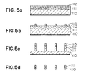
- Figs. 5a - 5d show a manufacturing process of grids used in a neutral beam etching apparatus of the present invention.
- Figs. 6a and 6b show the construction of a grid electrode used in a neutral beam etching apparatus of the present invention.
- Figs. 7a - 7c show another construction of charged particle retarding means used in a neutral beam etching apparatus of the present invention.
- Fig. 8 shows the whole construction of a neutral beam etching apparatus of the present invention using a coaxial type ion beam radical source of a first type.
- Fig. 9 shows the whole construction of a neutral beam etching apparatus of the present invention using a coaxial type ion beam radical source of a second type.
- Fig. 10 shows the whole construction of a neutral beam etching apparatus according to the present invention featured in that an ion beam is generated using rf hollow cathode discharge plasma.
- a neutral beam etching apparatus in Fig. 3 is composed of a discharge tube 22 which generates plasma for extracting an ion beam, two plates of graphite multiaperture electrodes 23 for extracting an ion beam, a wave-guide 21 for supplying microwave power, a solenoid 26 for generating a magnetic field in a discharge tube region, a gas supply tube 24, discharge tubes 28 and 30 for producing radicals, wave-guides 35 and 36 for supplying microwave power, solenoids 27 and 29 for generating a magnetic field in the discharge tube region, a set of grids 31 which prevent charged particles from being incident on a specimen 32 to be etched, a gas supply tube 25 for generating radicals, a device 33 for controlling specimen temperature and a vacuum pump 34.
- two sets of plasma sources for generating radicals are provided, which have an object to supply radicals uniformly in the specimen. It is effectual to provide further a plurality of plasma sources for effecting such an object, but sufficient uniformity can be realized with one set of plasma source only when the specimen is small.
- An ion beam having energy of several hundred eV which is extracted through the multiaperture electrodes 23 is converted into a neutral beam at a fair rate by charge exchange reactions with background gas molecules until it reaches a charged particle retarding grid system 31, and a residual ion beam is checked by the operation of the charged particle retarding grid system.
- the neutral beam is incident on the specimen surface.
- a gas for obtaining a neutral beam may be of any type, but it is more preferable to use a rare gas such as Ne, Ar, Kr and Xe which has a comparatively large charge exchange sectional area in a low ion energy region at several hundred eV and lower for obtaining a neutral beam of high density.
- a rare gas such as Ne, Ar, Kr and Xe which has a comparatively large charge exchange sectional area in a low ion energy region at several hundred eV and lower for obtaining a neutral beam of high density.
- Such an optional gas is supplied into the discharge tube 22 from the gas supply tube 24.
- Metal or graphite is used normally as an electrode material, and a plurality of apertures each having a diameter d are arranged regularly.
- Two plates of multiaperture electrodes are usually installed at an interval l which satisfies the relationship l ⁇ d. Because, if the distance between two plates of multiaperture electrodes is narrow to show l ⁇ d, parallelism of equipotential surfaces between both electrodes is very poor, divergence of the extracted ion beam is large, and dispersion of energy of ions is also large.
- a multiaperture electrode of the present invention is characterized in that the thickness of a multiaperture electrode 84 installed on a downstream side of an ion beam flow is made two times and more as large as the diameter d of the aperture as shown in Fig. 4b.
- Typical voltages applied to multiaperture electrodes for extracting an ion beam are +200 to +600 V for the multiaperture electrode on the discharge tube side, and -30 to -100 V for another multiaperture electrode.
- voltages at 0 V (ground potential), -40 to -100 V, voltage higher than the voltage corresponding to ion energy by 50 - 150 V and 0 V are applied in order to four pieces of charged particle retarding grid system 31 starting from a grid located on the ion source side, respectively.
- the kinetic energy of the neutral beam is at 500 eV and below from such a viewpoint, too.
- a carbon film 111 is grown in the thickness of several ⁇ m to ten and several ⁇ m by plasma chemical vapor deposition (plasma CVD) using well-known methane gas plasma and the like on a silicon substrate 110.
- plasma CVD plasma chemical vapor deposition
- an SiO2 film 112 having the thickness of about 1 ⁇ m is formed thereon by a sputtering method (Fig. 5a).
- a photoresist mesh-pattern 113 having a line width of 20 ⁇ m and a line space of 200 ⁇ m is further formed thereon through an ordinary photolithography process (Fig. 5b).
- the specimen thus obtained is applied with etching in order of SiO2 film, carbon film and silicon substrate as shown in Fig. 5c using appropriate reaction gas plasma, respectively, using a plasma etching apparatus.
- etching is stopped after etching down to the depth of 100 to 150 ⁇ m.
- a mesh grid composed of two layers of carbon and silicon as shown in Fig. 5d can be formed.
- this grid has carbon of slow sputtering and etching rate as an upper layer, it has such features of less abrasion and long life time and holding mechanical strength as a grid with silicon in the lower layer.
- a silicon carbide film may be used in place of the SiO2 film 112 in the forming method of the grid.
- Another method of the present invention for forming carbon grids for retarding charged particles is as follows.
- fibers 130 each having a diameter of 10 - 20 ⁇ m with pitch, polyester and the like as the material are knitted first in a mesh form in a desired texture, typically so as to show a distance at 0.5 to 1.0 mm between fibers.
- This mesh is fixed on a graphite holder 131 so as to obtain a grid such as shown in Fig. 6. Furthermore, a plurality of these grids are put one upon another, and desired voltage is applied thereto respectively, thereby to have them function as a charged particle retarding grid system.
- a similar carbon grid may also be formed by knitting preformed carbon fibers in a mesh form.
- Still another method of the present invention having an object of retarding charged particles is to replace a part of a plurality of grids with a comb-type deflection plate.
- Fig. 7b shows a sketch of a comb-type deflection plate, in which a positive voltage and a negative voltage are applied to comb-type deflection plates 64 and 65 forming one set with two pieces which are arranged in a nest, respectively, for use.
- a comb-type deflection plate 63 As a sectional view shown in Fig. 7a, two pieces of grids 61 and 62 are arranged in front of a comb-type deflection plate 63, viz., in a direction toward an ion source, and ground potential is applied to the grid 61 and a negative voltage is applied to the grid 62, thereby to check incidence of electrons from plasma. Those ions that have positive charges are deflected by the comb-type deflection plate 63 and are lost after being incident on the surface of the deflection plate.
- either grid is etched gradually since a neutral beam collides therewith. Therefore, it is required to replace the grids with new ones periodically in order to maintain predetermined functions.
- a cassette including a plurality of required grids formed in one body is formed and new and old cassettes are exchanged for each other by movement from a preparation chamber.
- An Ar gas was introduced into the discharge tube 22 at a pressure of 0.1 Pa, plasma was generated by supplying microwave power at 200 W, and an Ar positive ion beam at 500 eV was extracted therefrom.
- the current density of the ion beam was 0.5 mA/cm2.
- This ion beam was converted into a neutral beam by approximately half until it reached a charged particle retarding electrode 31 which was apart from a multiaperture electrode 23 by 13 cm.
- a CHF3 gas was introduced at a partial pressure of 65 mPa from the gas supply tube 25, and plasma was generated by discharge tubes 28 and 30. It was found at that time that the ion beam current density and the neutral beam density increased 1.2 to 1.5 times as large as before due to generation of the plasma.
- the etching rate of SiO2 was approximately 8 nm/min when plasma was not generated by the discharge tubes 28 and 30, but it increased to approximately 80 nm/min when plasma was generated. In the case of the latter, the etching rate for silicon was approximately 10 nm/min, and the etching selective ratio for silicon was 8.
- a gas obtained by mixing SF6 and Cl2 at a ratio of 3:1 was introduced from the gas supply tube 25 in place of the CHF3 gas mentioned above so as to show a pressure at 80 mPa, thereby to generate plasma in the discharge tubes 28 and 30.
- the etching rate for silicon was 100 to 150 nm/min. This etching rate is about six times as fast as that in a case when plasma is not generated in the discharge tubes 28 and 30. It was confirmed that the etched cross-sectional configuration was rectangular and etching could be made perpendicularly.
- the charged particle retarding grid 31 is a grid made of carbon fibers formed by a method explained previously or having a two layer structure of carbon and silicon. The obtained etching characteristics were the same in the cases when either grid was used.
- a method of supplying microwave to a sidewall of a vacuum chamber of an etching apparatus can achieve the original object of increasing etching rate remarkably by supplying radicals of high density, but has two problems as follows.
- a first problem is the increase in manufacturing cost of the apparatus due to the fact that a plasma source for radical supply is provided separately from the ion beam source.
- a microwave generator a wave-guide, a discharge tube, a magnetic field generator for operating cyclotron motion of electrons and so forth are required in order to generate plasma with microwave.
- a plasma generator for an ion beam source, the manufacturing cost of the apparatus may be curtailed by that portion.
- a second drawback is such that, when a unit for generating microwave plasma is provided on a sidewall of a vacuum chamber, a direction of required magnetic field takes a direction normal to or close to normal to the direction of an ion beam and a neutral beam, and thus, a path of an ion beam before neutralized by charge exchange is bent by Lorentz force.
- the beam direction diverges, thus lowering the etching rate or harming the etching direction.
- Fig. 8 shows an embodiment of a neutral beam etching apparatus using a coaxial type ion-beam and radical source according to the present invention.
- a coaxial ion-beam and radical source includes a first wave-guide 1 and a second wave-guide 2. These two wave-guides have a coaxial type double structure starting on the way, and microwave is supplied to each of them independently.
- the etching apparatus shown in the figure consists of a discharge tube 6, a set of solenoids 4 arranged coaxially, a multiaperture electrode 3 for extracting an ion beam, gas supply pipes 5 and 7, a set of charged particle retarding grids 8, a device 10 for controlling the temperature of a specimen 9 and an evacuation device 11 in addition to those wave-guides.
- a set of solenoids 4 are arranged coaxially, that a plasma generating region for supplying radicals is provided in the peripheral portion of the discharge tube 6 for extracting an ion beam, and that wave-guides for microwaves supplied to both are formed into a duplex tube and microwave power is supplied to each of them independently.
- This is referred to as a "coaxial type ion-beam and radical source" in the present invention.
- an ion beam make a flight for a certain distance (for example, 10 cm and more) in order to convert an ion beam into a neutral beam.
- the multiaperture electrode 3 for extracting an ion beam was installed at a position farther from the specimen than a generating region 12 of plasma for supplying radicals as shown in Fig. 8.
- the discharge tube 6 which is composed of a dielectric such as quartz and alumina, and plasma is generated therein.
- a positive voltage and a negative voltage are applied to two plates of multiaperture electrodes 3, respectively, whereby an ion beam at desired energy can be extracted from the plasma.
- the microwave supplied to the first wave-guide 1 serves to generate plasma in a chamber 12 in front of the specimen 9.
- the magnetic field produced by a group of electromagnets 4 can be made almost parallel to the direction of an ion beam extracted from the multiaperture electrode 3, the ion beam before neutralization will never be deflected largely by means of the magnetic field.
- a second type of coaxial type plasma source supplies microwave which generates both plasma for forming an ion beam and plasma for supplying radicals with a single wave-guide 41 as shown in Fig. 9.
- a discharge tube 42 is divided into the inner part and the outer part, and a multiaperture electrode 44 which extracts an ion beam is installed in the inner part portion.
- the outer part portion is a region for generating plasma for supplying radicals.
- the first type is excellent in such a point that the microwave intensity supplied to plasma sources of both microwave attenuators can be controlled independently, but the microwave intensity can be controlled to some extent by providing a microwave attenuator in the wave-guide in the second type, too.
- the specimen was etched at respective temperatures at 40°C and below by controlling the specimen temperature in etching using apparatus in the embodiments 1, 2 and 3.
- the specimen was a silicon wafer for composing a semiconductor integrated circuit including a MOS (metal-oxide semiconductor) capacitor and a MOS transistor.
- MOS metal-oxide semiconductor
- the life time of a MOS transistor means voltage application time to exceed a certain permissible shift as to a phenomenon in which a threshold voltage of a MOS transistor shifts when a certain voltage is applied for a long time to each of a source, a gate, a drain and a substrate which compose the MOS transistor.
- Etching of silicon was carried out using the apparatus shown in Fig. 3 in a similar manner as the Embodiment 1.
- a excimer laser light using KrF was radiated to the front of a charged particle retarding electrode through a window on a sidewall of the apparatus instead of generating plasma for supplying neutral radicals, thus exciting molecules of SF6 + Cl2 gas by laser light.
- Other conditions were set similarly to those of silicon etching example in the Embodiment 1.
- the silicon etching rate in the case of no irradiation with laser light, viz., by a neutral beam only was 15 - 30 m/min, but was increased to 1.5 - 2 times by irradiation with laser light.
- the silicon etching rate was also increased to about 1.5 times thereof.
- the line space of grids of the charged particle retarding grids arranged in front of the specimen may be as large as 1 - 2 mm because it is only required to retard proceeding of only an ion beam and a few electrons remaining in a neutral beam.
- a central axis 104 of a specimen rest 103 was inclined by an angle 8 with respect to a direction 101 of a neutral beam as shown in Fig. 2 so that the neutral beam would be incident from a direction with a slight gradient with respect to a direction normal to the specimen surface.
- ⁇ was set at an optional angle between 3° and 15°.
- a function of rotating the specimen rest 103 was added, thereby to rotate the specimen during etching.
- the rotating speed was set between 10 rpm and 100 rpm.
- Fig. 1 is an external view of an etched specimen, in which it is shown that etching residue 96 is produced along a bottom portion of a step portion 92 in polysilicon 94.
- a mixed gas plasma of SiH4 + N2O at a pressure of approximately 0.13 Pa was generated.
- An insulating film containing Si and O as principal components has grown by chemical reactions on a surface generated when neutral molecules only in plasma reached the specimen surface.
- the temperature of the specimen that time was maintained at a constant value between 100°C and 400°C.
- the temperature of the specimen while the insulating film is growing is as high as 300 - 500°C in general, which is advantageous for forming a dense and uniform film.
- a dense and uniform film can also be formed at a lower temperature of 100 - 200°C.
- a neutral beam etching apparatus shown in Fig. 10 shows an embodiment characterized in that an rf hollow cathode discharge plasma is used in a portion of generating an ion beam in place of a system using microwave excitation plasma shown in Fig. 3, Fig. 8 and Fig. 9.
- the kinetic energy of ions in the ion beam can be controlled by a potential applied to the anode, and the higher the positive potential is, the higher the energy of the generated ion beam becomes.
- the kinetic energy of neutral particles can also be increased when the ion beam is converted into a neutral beam by charge exchange reactions.
- ions of high density collide with the internal surface of the hollow cathode 122 at a comparatively high energy of several hundred eV. Therefore, the hollow cathode is heated to a very high temperature as well as consumed by etching.
- graphite is adopted as the material for the hollow cathode 122 and the multiaperture 124.
- the present invention is a very effectual technique in a point that defects such as insulation breakdown and charge accumulation in film of a very thin insulating film scarcely occur.
- a system composing the present invention it is possible to curtail the manufacturing cost and the working cost of the apparatus by a large margin by simplifying the structure of an apparatus for surface treatment for etching, deposition and so on using a neutral beam, and also to suppress divergence of the neutral beam, thereby enabling uniform surface treatment.
- the density of the neutral beam which is finally obtainable can be increased, and the surface treatment speed can also be increased.
Landscapes
- Physics & Mathematics (AREA)
- Engineering & Computer Science (AREA)
- Plasma & Fusion (AREA)
- Chemical & Material Sciences (AREA)
- Analytical Chemistry (AREA)
- Drying Of Semiconductors (AREA)
Applications Claiming Priority (2)
| Application Number | Priority Date | Filing Date | Title |
|---|---|---|---|
| JP41004/90 | 1990-02-23 | ||
| JP4100490 | 1990-02-23 |
Publications (2)
| Publication Number | Publication Date |
|---|---|
| EP0443154A2 true EP0443154A2 (fr) | 1991-08-28 |
| EP0443154A3 EP0443154A3 (en) | 1992-01-02 |
Family
ID=12596257
Family Applications (1)
| Application Number | Title | Priority Date | Filing Date |
|---|---|---|---|
| EP19900124468 Withdrawn EP0443154A3 (en) | 1990-02-23 | 1990-12-17 | Apparatus for and method of surface treatment for microelectronic devices |
Country Status (4)
| Country | Link |
|---|---|
| US (1) | US5284544A (fr) |
| EP (1) | EP0443154A3 (fr) |
| JP (1) | JPH04180621A (fr) |
| KR (1) | KR910016054A (fr) |
Cited By (15)
| Publication number | Priority date | Publication date | Assignee | Title |
|---|---|---|---|---|
| EP0522296A3 (en) * | 1991-06-10 | 1993-03-10 | Kawasaki Steel Corporation | Plasma processing system and method |
| EP0528655A3 (fr) * | 1991-08-16 | 1994-03-23 | Hitachi Ltd | |
| WO1994029494A1 (fr) * | 1993-06-04 | 1994-12-22 | Applied Science Technology | Generateur de plasma a micro-ondes |
| WO1996015545A1 (fr) * | 1994-11-15 | 1996-05-23 | Mattson Technology, Inc. | Reacteur a plasma inductif |
| WO1996025755A1 (fr) * | 1995-02-16 | 1996-08-22 | Plasmion | Dispositif a resonance cyclotron electronique pour creer un faisceau d'ions |
| EP0789506A1 (fr) * | 1996-02-09 | 1997-08-13 | Nihon Shinku Gijutsu Kabushiki Kaisha | Dispositif pour engendrer et utiliser un plasma du type à décharge suivant une ligne magnétiquement neutre |
| EP0740327A3 (fr) * | 1995-04-28 | 1998-03-04 | Hitachi, Ltd. | Appareil de traitement par faisceau d'ions |
| WO1999001888A1 (fr) * | 1997-07-02 | 1999-01-14 | Tokyo Electron Arizona, Inc. | Appareil et procede pour un traitement au plasma anisotrope, uniforme et a faibles deteriorations |
| EP0964425A3 (fr) * | 1998-06-09 | 2004-02-11 | Hitachi, Ltd. | Apparaeil pour le traitement d'une cible par un faisceau d'ions uniformement neutralisé |
| WO2005053365A1 (fr) * | 2003-11-27 | 2005-06-09 | Sem Technology Co., Ltd | Appareil de traitement de faisceau de particules neutres |
| WO2007034239A3 (fr) * | 2005-09-19 | 2008-10-09 | Owlstone Ltd | Pompe ionique |
| US7604708B2 (en) | 2003-02-14 | 2009-10-20 | Applied Materials, Inc. | Cleaning of native oxide with hydrogen-containing radicals |
| FR3011712A1 (fr) * | 2013-10-07 | 2015-04-10 | Riber | Source plasma radiofrequence a couplage inductif |
| US9136794B2 (en) | 2011-06-22 | 2015-09-15 | Research Triangle Institute, International | Bipolar microelectronic device |
| EP2933822A1 (fr) * | 2014-04-17 | 2015-10-21 | Zavtrod Innovation Corporation | Système de gravure physique sans contact |
Families Citing this family (111)
| Publication number | Priority date | Publication date | Assignee | Title |
|---|---|---|---|---|
| JP2888258B2 (ja) * | 1990-11-30 | 1999-05-10 | 東京エレクトロン株式会社 | 基板処理装置および基板処理方法 |
| US5217570A (en) * | 1991-01-31 | 1993-06-08 | Sony Corporation | Dry etching method |
| JPH05251408A (ja) * | 1992-03-06 | 1993-09-28 | Ebara Corp | 半導体ウェーハのエッチング装置 |
| CH686254A5 (de) * | 1992-07-27 | 1996-02-15 | Balzers Hochvakuum | Verfahren zur Einstellung der Bearbeitungsratenverteilung sowie Aetz- oder Plasma-CVD-Anlage zu dessen Ausfuehrung. |
| US5580808A (en) * | 1992-07-30 | 1996-12-03 | Canon Kabushiki Kaisha | Method of manufacturing a ROM device having contact holes treated with hydrogen atoms and energy beam |
| US5462629A (en) * | 1992-08-28 | 1995-10-31 | Kawasaki Steel Corp. | Surface processing apparatus using neutral beam |
| US5413954A (en) * | 1992-11-10 | 1995-05-09 | At&T Bell Laboratories | Method of making a silicon-based device comprising surface plasma cleaning |
| US5556475A (en) * | 1993-06-04 | 1996-09-17 | Applied Science And Technology, Inc. | Microwave plasma reactor |
| JP2611732B2 (ja) * | 1993-12-13 | 1997-05-21 | 日本電気株式会社 | プラズマ処理装置 |
| JPH07245193A (ja) * | 1994-03-02 | 1995-09-19 | Nissin Electric Co Ltd | プラズマ発生装置及びプラズマ処理装置 |
| JP3438109B2 (ja) * | 1994-08-12 | 2003-08-18 | 富士通株式会社 | プラズマ処理装置及びプラズマ処理方法 |
| US5637188A (en) * | 1995-02-17 | 1997-06-10 | Colorado Seminary | Processing substrates with a photon-enhanced neutral beam |
| US6375860B1 (en) * | 1995-03-10 | 2002-04-23 | General Atomics | Controlled potential plasma source |
| EP0846190A1 (fr) * | 1995-06-13 | 1998-06-10 | Massively Parallel Instruments, Inc. | Elements d'optique ioniques paralleles perfectionnes et appareil pour faisceaux ioniques de faible puissance et de courant eleve |
| US5630880A (en) * | 1996-03-07 | 1997-05-20 | Eastlund; Bernard J. | Method and apparatus for a large volume plasma processor that can utilize any feedstock material |
| US5614026A (en) * | 1996-03-29 | 1997-03-25 | Lam Research Corporation | Showerhead for uniform distribution of process gas |
| US5814154A (en) * | 1997-01-23 | 1998-09-29 | Gasonics International | Short-coupled-path extender for plasma source |
| JPH10223607A (ja) * | 1997-02-03 | 1998-08-21 | Mitsubishi Electric Corp | プラズマ処理装置 |
| JP3317209B2 (ja) * | 1997-08-12 | 2002-08-26 | 東京エレクトロンエイ・ティー株式会社 | プラズマ処理装置及びプラズマ処理方法 |
| JP3027968B2 (ja) * | 1998-01-29 | 2000-04-04 | 日新電機株式会社 | 成膜装置 |
| US6352049B1 (en) | 1998-02-09 | 2002-03-05 | Applied Materials, Inc. | Plasma assisted processing chamber with separate control of species density |
| US6635578B1 (en) | 1998-02-09 | 2003-10-21 | Applied Materials, Inc | Method of operating a dual chamber reactor with neutral density decoupled from ion density |
| US6039000A (en) | 1998-02-11 | 2000-03-21 | Micrion Corporation | Focused particle beam systems and methods using a tilt column |
| JP2976965B2 (ja) * | 1998-04-02 | 1999-11-10 | 日新電機株式会社 | 成膜方法及び成膜装置 |
| EP0999573B1 (fr) * | 1998-11-06 | 2006-06-28 | ICT Integrated Circuit Testing Gesellschaft für Halbleiterprüftechnik mbH | Colonne de faisceau de particules chargées |
| US6175095B1 (en) * | 1999-03-18 | 2001-01-16 | Gasonics International | Resonant impedance-matching slow-wave ring structure microwave applicator for plasmas |
| US7094312B2 (en) | 1999-07-22 | 2006-08-22 | Fsi Company | Focused particle beam systems and methods using a tilt column |
| US20010046566A1 (en) * | 2000-03-23 | 2001-11-29 | Chu Paul K. | Apparatus and method for direct current plasma immersion ion implantation |
| US6498107B1 (en) * | 2000-05-01 | 2002-12-24 | Epion Corporation | Interface control for film deposition by gas-cluster ion-beam processing |
| JP4730572B2 (ja) * | 2000-08-21 | 2011-07-20 | 株式会社アルバック | プラズマ成膜装置及びそのクリーニング方法 |
| KR100382720B1 (ko) * | 2000-08-30 | 2003-05-09 | 삼성전자주식회사 | 반도체 식각 장치 및 이를 이용한 반도체 소자의 식각 방법 |
| KR100380660B1 (ko) * | 2000-11-22 | 2003-04-18 | 학교법인 성균관대학 | 중성빔을 이용한 반도체소자의 식각방법 및 이를 위한식각장치 |
| US7111629B2 (en) * | 2001-01-08 | 2006-09-26 | Apl Co., Ltd. | Method for cleaning substrate surface |
| US20020124867A1 (en) * | 2001-01-08 | 2002-09-12 | Apl Co., Ltd. | Apparatus and method for surface cleaning using plasma |
| JP3912993B2 (ja) * | 2001-03-26 | 2007-05-09 | 株式会社荏原製作所 | 中性粒子ビーム処理装置 |
| WO2002091809A2 (fr) * | 2001-05-03 | 2002-11-14 | Apit Corp. S.A. | Procede et dispositif de generation d'un rideau de gaz active pour traitement de surface |
| KR100421415B1 (ko) * | 2001-09-12 | 2004-03-09 | 한국전자통신연구원 | 반도체 제조장비의 샘플 홀더 구동장치 및 이를 이용한 에칭방법 |
| US6914005B2 (en) * | 2002-03-01 | 2005-07-05 | Hitachi High-Technologies Corporation | Plasma etching method |
| US7998537B2 (en) * | 2002-03-01 | 2011-08-16 | The Chinese University Of Hong Kong | Method for selectively removing hydrogen from molecules |
| US6932518B2 (en) * | 2002-03-19 | 2005-08-23 | Finisar Corporation | Circuit board having traces with distinct transmission impedances |
| US7254149B2 (en) | 2002-03-19 | 2007-08-07 | Finisar Corporation | Submount, pedestal, and bond wire assembly for a transistor outline package with reduced bond wire inductance |
| US7042067B2 (en) * | 2002-03-19 | 2006-05-09 | Finisar Corporation | Transmission line with integrated connection pads for circuit elements |
| US7044657B2 (en) * | 2002-03-19 | 2006-05-16 | Finisar Corporation | Transistor outline package with exteriorly mounted resistors |
| US7013834B2 (en) * | 2002-04-19 | 2006-03-21 | Nordson Corporation | Plasma treatment system |
| JP4134312B2 (ja) * | 2002-04-23 | 2008-08-20 | 独立行政法人産業技術総合研究所 | 分子ビーム装置 |
| EP1361437A1 (fr) * | 2002-05-07 | 2003-11-12 | Centre National De La Recherche Scientifique (Cnrs) | Un nouveau marqueur biologique pour des tumeurs et des méthodes pour la détection de phénotype cancéreux ou non-cancéreux de cellules |
| US20060233682A1 (en) * | 2002-05-08 | 2006-10-19 | Cherian Kuruvilla A | Plasma-assisted engine exhaust treatment |
| JP2005524963A (ja) * | 2002-05-08 | 2005-08-18 | ダナ・コーポレーション | プラズマ触媒 |
| US20060237398A1 (en) * | 2002-05-08 | 2006-10-26 | Dougherty Mike L Sr | Plasma-assisted processing in a manufacturing line |
| US7638727B2 (en) * | 2002-05-08 | 2009-12-29 | Btu International Inc. | Plasma-assisted heat treatment |
| US7504061B2 (en) * | 2002-05-08 | 2009-03-17 | Leonhard Kurz Gmbh & Co., Kg | Method of decorating large plastic 3D objects |
| US7497922B2 (en) * | 2002-05-08 | 2009-03-03 | Btu International, Inc. | Plasma-assisted gas production |
| US20060062930A1 (en) * | 2002-05-08 | 2006-03-23 | Devendra Kumar | Plasma-assisted carburizing |
| US7445817B2 (en) * | 2002-05-08 | 2008-11-04 | Btu International Inc. | Plasma-assisted formation of carbon structures |
| US7432470B2 (en) | 2002-05-08 | 2008-10-07 | Btu International, Inc. | Surface cleaning and sterilization |
| US20050233091A1 (en) * | 2002-05-08 | 2005-10-20 | Devendra Kumar | Plasma-assisted coating |
| US20060057016A1 (en) * | 2002-05-08 | 2006-03-16 | Devendra Kumar | Plasma-assisted sintering |
| US20060228497A1 (en) * | 2002-05-08 | 2006-10-12 | Satyendra Kumar | Plasma-assisted coating |
| US7465362B2 (en) * | 2002-05-08 | 2008-12-16 | Btu International, Inc. | Plasma-assisted nitrogen surface-treatment |
| US7494904B2 (en) * | 2002-05-08 | 2009-02-24 | Btu International, Inc. | Plasma-assisted doping |
| US7560657B2 (en) * | 2002-05-08 | 2009-07-14 | Btu International Inc. | Plasma-assisted processing in a manufacturing line |
| US7498066B2 (en) * | 2002-05-08 | 2009-03-03 | Btu International Inc. | Plasma-assisted enhanced coating |
| US6661009B1 (en) | 2002-05-31 | 2003-12-09 | Fei Company | Apparatus for tilting a beam system |
| AU2003263746A1 (en) * | 2002-07-03 | 2004-01-23 | Tokyo Electron Limited | Method and apparatus for non-invasive measurement and analysis of semiconductor process parameters |
| AU2003247538A1 (en) * | 2002-07-03 | 2004-01-23 | Tokyo Electron Limited | Method and apparatus for non-invasive measurement and analys of semiconductor plasma parameters |
| US6863930B2 (en) | 2002-09-06 | 2005-03-08 | Delphi Technologies, Inc. | Refractory metal mask and methods for coating an article and forming a sensor |
| US7189940B2 (en) | 2002-12-04 | 2007-03-13 | Btu International Inc. | Plasma-assisted melting |
| DE10260745A1 (de) * | 2002-12-23 | 2004-07-01 | Outokumpu Oyj | Verfahren und Anlage zur thermischen Behandlung von körnigen Feststoffen |
| US7355687B2 (en) * | 2003-02-20 | 2008-04-08 | Hunter Engineering Company | Method and apparatus for vehicle service system with imaging components |
| US7232767B2 (en) * | 2003-04-01 | 2007-06-19 | Mattson Technology, Inc. | Slotted electrostatic shield modification for improved etch and CVD process uniformity |
| US6812647B2 (en) * | 2003-04-03 | 2004-11-02 | Wayne D. Cornelius | Plasma generator useful for ion beam generation |
| US20050187374A1 (en) * | 2004-02-20 | 2005-08-25 | Bin Chen | Polyester synthesis with enhanced titanium catalyst composition |
| US20050211171A1 (en) * | 2004-03-26 | 2005-09-29 | Applied Materials, Inc. | Chemical vapor deposition plasma reactor having an ion shower grid |
| US20050211546A1 (en) * | 2004-03-26 | 2005-09-29 | Applied Materials, Inc. | Reactive sputter deposition plasma process using an ion shower grid |
| US7695590B2 (en) * | 2004-03-26 | 2010-04-13 | Applied Materials, Inc. | Chemical vapor deposition plasma reactor having plural ion shower grids |
| US7244474B2 (en) * | 2004-03-26 | 2007-07-17 | Applied Materials, Inc. | Chemical vapor deposition plasma process using an ion shower grid |
| US7291360B2 (en) * | 2004-03-26 | 2007-11-06 | Applied Materials, Inc. | Chemical vapor deposition plasma process using plural ion shower grids |
| US20050211547A1 (en) * | 2004-03-26 | 2005-09-29 | Applied Materials, Inc. | Reactive sputter deposition plasma reactor and process using plural ion shower grids |
| US7767561B2 (en) * | 2004-07-20 | 2010-08-03 | Applied Materials, Inc. | Plasma immersion ion implantation reactor having an ion shower grid |
| US8058156B2 (en) * | 2004-07-20 | 2011-11-15 | Applied Materials, Inc. | Plasma immersion ion implantation reactor having multiple ion shower grids |
| EP1630849B1 (fr) * | 2004-08-27 | 2011-11-02 | Fei Company | Traitement localisé par plasma |
| US20060042752A1 (en) * | 2004-08-30 | 2006-03-02 | Rueger Neal R | Plasma processing apparatuses and methods |
| WO2006127037A2 (fr) * | 2004-11-05 | 2006-11-30 | Dana Corporation | Traitement atmospherique effectue au moyen de plasmas generes par des micro-ondes |
| KR100668075B1 (ko) * | 2005-03-24 | 2007-01-15 | 성균관대학교산학협력단 | 중성빔 식각장치를 이용한 식각방법 |
| US20070114123A1 (en) * | 2005-11-21 | 2007-05-24 | Jeffrey Bender | Deposition on charge sensitive materials with ion beam deposition |
| KR100868019B1 (ko) | 2007-01-30 | 2008-11-10 | 삼성전자주식회사 | 플라즈마 쉬쓰 제어기를 갖는 이온 빔 장치 |
| US20090084501A1 (en) * | 2007-09-27 | 2009-04-02 | Tokyo Electron Limited | Processing system for producing a negative ion plasma |
| JP2010020841A (ja) * | 2008-07-10 | 2010-01-28 | Showa Denko Kk | インライン式成膜装置及び磁気記録媒体の製造方法 |
| US20100270262A1 (en) * | 2009-04-22 | 2010-10-28 | Applied Materials, Inc. | Etching low-k dielectric or removing resist with a filtered ionized gas |
| US8222125B2 (en) * | 2010-08-12 | 2012-07-17 | Ovshinsky Innovation, Llc | Plasma deposition of amorphous semiconductors at microwave frequencies |
| US8617411B2 (en) * | 2011-07-20 | 2013-12-31 | Lam Research Corporation | Methods and apparatus for atomic layer etching |
| WO2013024915A1 (fr) * | 2011-08-17 | 2013-02-21 | 삼성전자주식회사 | Appareil de pulvérisation et procédé de formation d'une couche conductrice transmissive d'un dispositif électroluminescent |
| KR101526507B1 (ko) * | 2013-11-15 | 2015-06-09 | 피에스케이 주식회사 | 기판 처리 장치 및 방법 |
| US9837254B2 (en) | 2014-08-12 | 2017-12-05 | Lam Research Corporation | Differentially pumped reactive gas injector |
| US10825652B2 (en) * | 2014-08-29 | 2020-11-03 | Lam Research Corporation | Ion beam etch without need for wafer tilt or rotation |
| US9406535B2 (en) * | 2014-08-29 | 2016-08-02 | Lam Research Corporation | Ion injector and lens system for ion beam milling |
| US9536748B2 (en) | 2014-10-21 | 2017-01-03 | Lam Research Corporation | Use of ion beam etching to generate gate-all-around structure |
| SG11201610529QA (en) | 2015-03-16 | 2017-01-27 | Canon Anelva Corp | Grid, method of manufacturing the same, and ion beam processing apparatus |
| JP6434617B2 (ja) | 2015-05-22 | 2018-12-05 | 株式会社日立ハイテクノロジーズ | プラズマ処理装置およびそれを用いたプラズマ処理方法 |
| US9779955B2 (en) | 2016-02-25 | 2017-10-03 | Lam Research Corporation | Ion beam etching utilizing cryogenic wafer temperatures |
| KR102066222B1 (ko) | 2017-10-30 | 2020-01-14 | 대전대학교 산학협력단 | 저차원 물질을 위한 표면처리 방법 |
| US10847374B2 (en) | 2017-10-31 | 2020-11-24 | Lam Research Corporation | Method for etching features in a stack |
| FR3073954B1 (fr) * | 2017-11-20 | 2019-12-20 | Commissariat A L'energie Atomique Et Aux Energies Alternatives | Systeme de transduction d'un deplacement en un dephasage optique. |
| JP6902991B2 (ja) | 2017-12-19 | 2021-07-14 | 株式会社日立ハイテク | プラズマ処理装置 |
| US10361092B1 (en) | 2018-02-23 | 2019-07-23 | Lam Research Corporation | Etching features using metal passivation |
| KR20250011246A (ko) | 2019-02-28 | 2025-01-21 | 램 리써치 코포레이션 | 측벽 세정을 사용한 이온 빔 에칭 |
| US11776792B2 (en) | 2020-04-03 | 2023-10-03 | Hitachi High-Tech Corporation | Plasma processing apparatus and plasma processing method |
| KR102521388B1 (ko) | 2020-04-21 | 2023-04-14 | 주식회사 히타치하이테크 | 플라스마 처리 장치 |
| JP7598443B2 (ja) | 2022-03-07 | 2024-12-11 | 株式会社日立ハイテク | プラズマ処理方法 |
| KR102826180B1 (ko) | 2022-04-26 | 2025-06-27 | 주식회사 히타치하이테크 | 플라스마 처리 방법 |
| US20230369022A1 (en) * | 2022-05-13 | 2023-11-16 | Applied Materials, Inc. | Recombination channels for angle control of neutral reactive species |
Family Cites Families (21)
| Publication number | Priority date | Publication date | Assignee | Title |
|---|---|---|---|---|
| EP0106497B1 (fr) * | 1982-09-10 | 1988-06-01 | Nippon Telegraph And Telephone Corporation | Appareil d'arrosage ionique |
| JPH0770509B2 (ja) * | 1982-10-08 | 1995-07-31 | 株式会社日立製作所 | ドライプロセス装置 |
| JPS5998478A (ja) * | 1982-11-26 | 1984-06-06 | Nippon Denso Co Ltd | 有機電池 |
| JPS59159167A (ja) * | 1983-03-01 | 1984-09-08 | Zenko Hirose | アモルフアスシリコン膜の形成方法 |
| JPS6175529A (ja) * | 1984-09-21 | 1986-04-17 | Toshiba Corp | ドライエツチング方法及び装置 |
| US4678681A (en) * | 1984-10-05 | 1987-07-07 | Hiraoka & Co. Ltd. | Process for preparation of water-proof sheets |
| JPS61136229A (ja) * | 1984-12-06 | 1986-06-24 | Toshiba Corp | ドライエツチング装置 |
| JPS61141141A (ja) * | 1984-12-14 | 1986-06-28 | Hitachi Ltd | ドライエツチング装置 |
| JPS61144827A (ja) * | 1984-12-19 | 1986-07-02 | Hitachi Ltd | ドライエツチング装置 |
| US4761199A (en) * | 1985-04-10 | 1988-08-02 | Canon Kabushiki Kaisha | Shutter device for ion beam etching apparatus and such etching apparatus using same |
| US4687544A (en) * | 1985-05-17 | 1987-08-18 | Emergent Technologies Corporation | Method and apparatus for dry processing of substrates |
| JPS6233422A (ja) * | 1985-08-06 | 1987-02-13 | Fujitsu Ltd | シリコンカ−バイドのエピタキシヤル成長方法 |
| JPS62122219A (ja) * | 1985-11-22 | 1987-06-03 | Hitachi Ltd | イオンビ−ムエツチング装置 |
| US5022977A (en) * | 1986-09-29 | 1991-06-11 | Nippon Telegraph And Telephone Corporation | Ion generation apparatus and thin film forming apparatus and ion source utilizing the ion generation apparatus |
| US4869780A (en) * | 1987-04-10 | 1989-09-26 | Trw Inc. | Ion milling method |
| US4956043A (en) * | 1987-05-25 | 1990-09-11 | Hitachi, Ltd. | Dry etching apparatus |
| JPH0715602B2 (ja) * | 1987-06-15 | 1995-02-22 | 富士ゼロックス株式会社 | コロナ帯電装置 |
| JPS6487789A (en) * | 1987-09-30 | 1989-03-31 | Hitachi Ltd | Ion beam processing device |
| JPH01105460A (ja) * | 1987-10-16 | 1989-04-21 | Nippon Denso Co Ltd | 電池 |
| US4778561A (en) * | 1987-10-30 | 1988-10-18 | Veeco Instruments, Inc. | Electron cyclotron resonance plasma source |
| JPH0244720A (ja) * | 1988-08-05 | 1990-02-14 | Fujitsu Ltd | マイクロ波プラズマ処理装置 |
-
1990
- 1990-02-27 KR KR1019900021883A patent/KR910016054A/ko not_active Abandoned
- 1990-10-17 US US07/599,018 patent/US5284544A/en not_active Expired - Fee Related
- 1990-10-19 JP JP2278994A patent/JPH04180621A/ja active Pending
- 1990-12-17 EP EP19900124468 patent/EP0443154A3/en not_active Withdrawn
Cited By (25)
| Publication number | Priority date | Publication date | Assignee | Title |
|---|---|---|---|---|
| US5518572A (en) * | 1991-06-10 | 1996-05-21 | Kawasaki Steel Corporation | Plasma processing system and method |
| EP0522296A3 (en) * | 1991-06-10 | 1993-03-10 | Kawasaki Steel Corporation | Plasma processing system and method |
| EP0528655A3 (fr) * | 1991-08-16 | 1994-03-23 | Hitachi Ltd | |
| US5409562A (en) * | 1991-08-16 | 1995-04-25 | Hitachi, Ltd. | Dry-etching method and apparatus |
| WO1994029494A1 (fr) * | 1993-06-04 | 1994-12-22 | Applied Science Technology | Generateur de plasma a micro-ondes |
| JPH10508985A (ja) * | 1994-11-15 | 1998-09-02 | マットソン テクノロジー インコーポレーテッド | 誘導性プラズマリアクター |
| WO1996015545A1 (fr) * | 1994-11-15 | 1996-05-23 | Mattson Technology, Inc. | Reacteur a plasma inductif |
| US6551447B1 (en) | 1994-11-15 | 2003-04-22 | Mattson Technology, Inc. | Inductive plasma reactor |
| US6143129A (en) * | 1994-11-15 | 2000-11-07 | Mattson Technology, Inc. | Inductive plasma reactor |
| US5811022A (en) * | 1994-11-15 | 1998-09-22 | Mattson Technology, Inc. | Inductive plasma reactor |
| WO1996025755A1 (fr) * | 1995-02-16 | 1996-08-22 | Plasmion | Dispositif a resonance cyclotron electronique pour creer un faisceau d'ions |
| FR2730858A1 (fr) * | 1995-02-16 | 1996-08-23 | Plasmion | Dispositif a resonance cyclotron electronique pour creer un faisceau d'ions |
| EP0740327A3 (fr) * | 1995-04-28 | 1998-03-04 | Hitachi, Ltd. | Appareil de traitement par faisceau d'ions |
| EP1132946A1 (fr) * | 1995-04-28 | 2001-09-12 | Hitachi, Ltd. | Appareil de traitement par faisceau d'ions |
| EP0789506A1 (fr) * | 1996-02-09 | 1997-08-13 | Nihon Shinku Gijutsu Kabushiki Kaisha | Dispositif pour engendrer et utiliser un plasma du type à décharge suivant une ligne magnétiquement neutre |
| WO1999001888A1 (fr) * | 1997-07-02 | 1999-01-14 | Tokyo Electron Arizona, Inc. | Appareil et procede pour un traitement au plasma anisotrope, uniforme et a faibles deteriorations |
| EP0964425A3 (fr) * | 1998-06-09 | 2004-02-11 | Hitachi, Ltd. | Apparaeil pour le traitement d'une cible par un faisceau d'ions uniformement neutralisé |
| US7604708B2 (en) | 2003-02-14 | 2009-10-20 | Applied Materials, Inc. | Cleaning of native oxide with hydrogen-containing radicals |
| WO2005053365A1 (fr) * | 2003-11-27 | 2005-06-09 | Sem Technology Co., Ltd | Appareil de traitement de faisceau de particules neutres |
| US7381943B2 (en) | 2003-11-27 | 2008-06-03 | Korea Basic Science Institute | Neutral particle beam processing apparatus |
| CN100466879C (zh) * | 2003-11-27 | 2009-03-04 | 韩国基础科学支援研究院 | 中性粒子束处理设备 |
| WO2007034239A3 (fr) * | 2005-09-19 | 2008-10-09 | Owlstone Ltd | Pompe ionique |
| US9136794B2 (en) | 2011-06-22 | 2015-09-15 | Research Triangle Institute, International | Bipolar microelectronic device |
| FR3011712A1 (fr) * | 2013-10-07 | 2015-04-10 | Riber | Source plasma radiofrequence a couplage inductif |
| EP2933822A1 (fr) * | 2014-04-17 | 2015-10-21 | Zavtrod Innovation Corporation | Système de gravure physique sans contact |
Also Published As
| Publication number | Publication date |
|---|---|
| KR910016054A (ko) | 1991-09-30 |
| JPH04180621A (ja) | 1992-06-26 |
| EP0443154A3 (en) | 1992-01-02 |
| US5284544A (en) | 1994-02-08 |
Similar Documents
| Publication | Publication Date | Title |
|---|---|---|
| EP0443154A2 (fr) | Appareil et méthode pour le traitement de surface de dispositifs microélectroniques | |
| US5518572A (en) | Plasma processing system and method | |
| JP6382055B2 (ja) | 被処理体を処理する方法 | |
| DE68924413T2 (de) | Radiofrequenzinduktion/Mehrpolplasma-Bearbeitungsvorrichtung. | |
| JP6366454B2 (ja) | 被処理体を処理する方法 | |
| KR100555849B1 (ko) | 중성입자빔 처리장치 | |
| JP2001520433A (ja) | 加速された粒子を発生させる装置並びに方法 | |
| TWI478200B (zh) | 佈植碳離子之方法 | |
| CN118471789A (zh) | 腔室上光以通过减少化学成分改善刻蚀均匀性 | |
| US6259105B1 (en) | System and method for cleaning silicon-coated surfaces in an ion implanter | |
| US20210313154A1 (en) | System And Methods Using An Inline Surface Engineering Source | |
| US20190096632A1 (en) | Charged particle beam irradiation apparatus and method for reducing electrification of substrate | |
| EP3518268B1 (fr) | Source de particules chargées et procédé de nettoyage d'une source de particules chargées à l'aide de rétropulvérisation | |
| JP2000068227A (ja) | 表面処理方法および装置 | |
| Pu | Plasma etch equipment | |
| JPH0950984A (ja) | 表面処理方法 | |
| JPH05102083A (ja) | ドライエツチング方法及びそのための装置 | |
| KR102704743B1 (ko) | 식각 장치 및 이를 이용한 식각 방법 | |
| JP3363040B2 (ja) | 高速原子線源 | |
| JP5227734B2 (ja) | 基板の低エネルギー電子促進エッチング及びクリーニング方法及び装置 | |
| JP4607328B2 (ja) | 基板の低エネルギー電子促進エッチング及びクリーニング方法及び装置 | |
| US6787781B1 (en) | Arc chamber filament for ion implanter | |
| RU2316845C1 (ru) | Способ плазмохимического травления полупроводниковых и диэлектрических материалов | |
| JPH07335618A (ja) | プラズマプロセスの方法及びプラズマプロセス装置 | |
| JPS6134844A (ja) | 中性微細ビ−ムの照射装置 |
Legal Events
| Date | Code | Title | Description |
|---|---|---|---|
| PUAI | Public reference made under article 153(3) epc to a published international application that has entered the european phase |
Free format text: ORIGINAL CODE: 0009012 |
|
| AK | Designated contracting states |
Kind code of ref document: A2 Designated state(s): DE NL |
|
| PUAL | Search report despatched |
Free format text: ORIGINAL CODE: 0009013 |
|
| AK | Designated contracting states |
Kind code of ref document: A3 Designated state(s): DE NL |
|
| 17P | Request for examination filed |
Effective date: 19920427 |
|
| 17Q | First examination report despatched |
Effective date: 19940719 |
|
| GRAG | Despatch of communication of intention to grant |
Free format text: ORIGINAL CODE: EPIDOS AGRA |
|
| GRAG | Despatch of communication of intention to grant |
Free format text: ORIGINAL CODE: EPIDOS AGRA |
|
| GRAG | Despatch of communication of intention to grant |
Free format text: ORIGINAL CODE: EPIDOS AGRA |
|
| GRAH | Despatch of communication of intention to grant a patent |
Free format text: ORIGINAL CODE: EPIDOS IGRA |
|
| STAA | Information on the status of an ep patent application or granted ep patent |
Free format text: STATUS: THE APPLICATION IS DEEMED TO BE WITHDRAWN |
|
| 18D | Application deemed to be withdrawn |
Effective date: 19980428 |