EP0443439A2 - One-transistor-storage cell device and method for making the same - Google Patents
One-transistor-storage cell device and method for making the same Download PDFInfo
- Publication number
- EP0443439A2 EP0443439A2 EP91102082A EP91102082A EP0443439A2 EP 0443439 A2 EP0443439 A2 EP 0443439A2 EP 91102082 A EP91102082 A EP 91102082A EP 91102082 A EP91102082 A EP 91102082A EP 0443439 A2 EP0443439 A2 EP 0443439A2
- Authority
- EP
- European Patent Office
- Prior art keywords
- layer
- insulation layer
- conductive
- contact window
- bit line
- Prior art date
- Legal status (The legal status is an assumption and is not a legal conclusion. Google has not performed a legal analysis and makes no representation as to the accuracy of the status listed.)
- Granted
Links
Images


Classifications
-
- H—ELECTRICITY
- H10—SEMICONDUCTOR DEVICES; ELECTRIC SOLID-STATE DEVICES NOT OTHERWISE PROVIDED FOR
- H10W—GENERIC PACKAGES, INTERCONNECTIONS, CONNECTORS OR OTHER CONSTRUCTIONAL DETAILS OF DEVICES COVERED BY CLASS H10
- H10W20/00—Interconnections in chips, wafers or substrates
- H10W20/40—Interconnections external to wafers or substrates, e.g. back-end-of-line [BEOL] metallisations or vias connecting to gate electrodes
- H10W20/41—Interconnections external to wafers or substrates, e.g. back-end-of-line [BEOL] metallisations or vias connecting to gate electrodes characterised by their conductive parts
- H10W20/42—Vias, e.g. via plugs
-
- H—ELECTRICITY
- H10—SEMICONDUCTOR DEVICES; ELECTRIC SOLID-STATE DEVICES NOT OTHERWISE PROVIDED FOR
- H10B—ELECTRONIC MEMORY DEVICES
- H10B12/00—Dynamic random access memory [DRAM] devices
- H10B12/01—Manufacture or treatment
- H10B12/02—Manufacture or treatment for one transistor one-capacitor [1T-1C] memory cells
- H10B12/03—Making the capacitor or connections thereto
- H10B12/033—Making the capacitor or connections thereto the capacitor extending over the transistor
-
- H—ELECTRICITY
- H10—SEMICONDUCTOR DEVICES; ELECTRIC SOLID-STATE DEVICES NOT OTHERWISE PROVIDED FOR
- H10B—ELECTRONIC MEMORY DEVICES
- H10B12/00—Dynamic random access memory [DRAM] devices
- H10B12/30—DRAM devices comprising one-transistor - one-capacitor [1T-1C] memory cells
- H10B12/31—DRAM devices comprising one-transistor - one-capacitor [1T-1C] memory cells having a storage electrode stacked over the transistor
- H10B12/318—DRAM devices comprising one-transistor - one-capacitor [1T-1C] memory cells having a storage electrode stacked over the transistor the storage electrode having multiple segments
Definitions
- the invention relates to a one-transistor memory cell arrangement and a method for its production, in particular for highly integrated dynamic semiconductor memories.
- the basic structure for dynamic semiconductor memories based on the principle of the one-transistor cell consists of a MOS selection transistor and a storage capacitor with a storage capacity of 30 to 50 fF, which contains the logical information as a stored charge.
- the selection transistor can be controlled via a word line. Its drain region is connected to an electrode of the storage capacitor, while its source region is connected to the outside via a bit line with source regions of further memory cells lying in the bit line direction.
- the storage capacitors are generally formed as a planar arrangement by a highly doped substrate surface section, an overlying storage dielectric (usually silicon dioxide) and a polysilicon cell plate.
- STC trench or stack capacitor
- the STC cell concept is distinguished from the trench cell concept by the fact that the storage capacity is largely electrically decoupled from the active silicon. As a result, the active silicon generally remains morphologically undisturbed except for the contacting of a lower storage electrode.
- the substrate defects typical of the trench cell concepts or the technological measures generally required to eliminate these defects and the lateral interaction of adjacent storage capacities via the silicon substrate avoided in principle and guaranteed a natural, high ALPHA immunity without special measures.
- the storage capacitor consists of two stacked doped polysilicon layers with a storage dielectric in between.
- the lower polysilicon layer acts as a storage electrode and is connected to the drain region of the selection transistor.
- the upper polysilicon layer acts as a common cell plate of a memory matrix.
- the electrode stack overlaps the gate of the selection transistor (cf. Koyanagi, IEDM Tech. Dig. 1978, pp. 348-351).
- EP-PS 0191612 An improved STC variant is known from EP-PS 0191612, in which the cell plate overlaps the edge of the storage electrode, as a result of which its side flank is obtained as an area contribution for a higher storage capacity.
- the simultaneous filling of the bit line contact window with the production of the storage electrode also solves the problem of the bit line break on the flanks of the bit line contact window.
- EP-PS 0263941 these advantages can be increased by increasing the thickness of the storage electrode.
- EP-PS 0223616 a method in which a trench is produced by deepening the drain contact window into the silicon substrate by means of an RIE process, the topology of which also contributes to an increase in the capacitive area after the storage electrode layer has been deposited.
- An even larger storage capacity can be achieved by combining the relief contributions of a thick storage electrode and a trench in the drain contact window (IEDM Tech. Dig., 1988, pp. 600-603).
- the three-dimensional SIC variants listed produce a topological relief which makes it difficult to break off bit line contact when the bit line is passed over the storage capacitor.
- IEDM Tech. Dig. 1988, S. 596-599 a solution is known in which the bit line is carried out under the storage capacity.
- the bit line is produced after the selection transistor has been completed in such a way that the bit line is guided laterally past the later drain contact window for the storage electrode. This opens up the basic possibility of vertically enlarging the STG complex without problems with bit line structuring and contacting.
- an STC cell concept (“fin type”) is known from EP-PS 0295709, in which the storage electrode consists of a mutually contacted multiple polysilicon stack which overlaps the selection transistor. These polysilicon fins are enclosed on all sides by the storage dielectric and a common polysilicon cell plate.
- Ema u. a. describe in IEDM Tech. Dig. 1988, p.592-595 both possibilities of the bit line routing below and above a storage capacity of the "fin type".
- bit line For memories greater than or equal to 16 MdRAM, the bit line must be arranged under the STC complex. Such complexly structured storage electrodes are difficult to control in terms of production technology (cf. IEDM Tech. Dig. 1989, pp. 31-34). Inoue et al. a. ibid with an SSC cell concept for 64 MdRAM or 256 MdRAM, a solution in which the bit line is arranged under the STC complex and storage electrodes of the "fin type" overlap each other into neighboring cell areas.
- a disadvantage of the latter two solutions irrespective of whether the polysilicon fins forming the storage electrode stack overlap only the own cell area or also the neighboring cell areas, is that during processing a processing phase occurs in which the horizontally arranged polysilicon fins are exposed to several process steps in a cantilever manner are. These process steps, such as wet etching and cleaning steps, oxidation, insulator and polysilicon CVD deposition, represent significant mechanical, chemical, and thermal stresses for these sensitive, cantilevered storage electrode configurations.
- the fins are preferably very thin (less than or equal to 100 nm) with a large length to thickness ratio and only in line with the other fins of the same storage electrode or grown on the single-crystalline silicon substrate.
- the stability of such self-supporting storage electrodes is low and, as a result, the yield in the production of the storage cell is adversely affected.
- a further disadvantage is that the long and narrow spaces between the polysilicon fins lie parallel to the silicon substrate surface and can only be reached, for example, by wet etching and cleaning processes via shaft-shaped channels lying perpendicular to it. This results in unfavorable transport, removal and exchange conditions for liquid and gaseous media in the micro areas of the storage electrode configuration, in particular for the surface treatment of the self-supporting polysilicon fins by wet etching and cleaning processes, but also for the subsequent CVD coating processes for the storage insulator and the polysilicon cell plate .
- the aim of the invention is a one-transistor memory cell arrangement for dynamic semiconductor memories and a method for their production, which significantly improve the quality and stability of the storage electrodes of the STC complex with high reproducibility, increase the yield of the production process and ensure an increase in the packing density.
- the object of the invention is to create a one-transistor memory cell arrangement for dynamic semiconductor memories and a method for their production, which are suitable for liquid and gaseous media when carrying out wet etching and cleaning processes and also coating methods, in particular when designing the STC Ensure complex, favorable conditions and avoid an adjustment-related safety distance when the STC complex is arranged above the bit line.
- the object is achieved by a one-transistor memory cell for highly integrated dynamic semiconductor memories, consisting of field isolation regions and active surface areas of a single-crystalline substrate, in which a MOS field effect transistor with an all-round insulated word line and a source and drain region is integrated, as well as one above arranged in the word line and largely covering the area of the memory cell stack capacitor (STC) complex, which is connected with its storage electrode to the drain area and its upper electrode as Cell plate of all memory cells of a memory matrix block is formed and a bit line contacted with the source region, solved in that the memory electrode consists of conductive lamellae arranged perpendicular to the substrate surface on a common, conductive base plate, each of which in the memory cell layout has a self-contained and closed band, the Width corresponds to the wall thickness of the slats, represents that each of the slats, starting with an outermost slat, which is arranged within the storage cell, encloses a smaller one, with
- the base plate in the memory cell layout corresponds exactly to the area enclosed by the periphery of the outermost lamella.
- the memory cell arrangement is designed in such a way that the base plate consists of a plurality of conductive layers, the layer thickness of a lowermost conductive base plate layer being less than or equal to the wall thickness of the slats, and the base plate surface corresponding at least to the area enclosed by the periphery of the outermost slat, that a second conductive layer is arranged on the lowermost conductive base plate layer, the layer thickness of which corresponds to the wall thickness of the outermost lamella and the area of which corresponds to the circumference of the outermost lamella enclosed area corresponds exactly to the fact that a third conductive layer is arranged on the second conductive layer, the layer thickness of which corresponds to the wall thickness of the next inner lamella and whose area corresponds exactly to the area enclosed by the circumference of the next inner lamella, and that further conductive layers
- the memory cell arrangement is characterized in that the lamellae end at a uniform height above the level of the substrate surface, regardless of the relief of the base plate with which they are contacted and regardless of the relief of the memory cell elements arranged under the base plate.
- a further embodiment of the memory cell arrangement is characterized in that a bit line is arranged on the insulated stack capacitor complex, the part of the bit line lying in the source contact window being stamp-like and planarized with respect to the top of the stack capacitor complex, and in that the drain contacting of the memory electrode by direct contact of the base plate with the Drain area in a drain contact window of a lower insulator layer, which is arranged on the isolated word lines and over the remaining memory cell regions with the exception of the contact windows of the source and drain regions.
- the memory cell arrangement is characterized in that the bit line covered with an upper insulation layer is arranged below the stack capacitor complex, the bit line being arranged on the lower insulation layer above the word line insulation and the lower insulation layer all regions of the memory cell, except the source and drain contact window area, covers that the bit line in the source contact window contacts the source area and that an insulated conductive Stamp that contacts the drain area in the drain contact window, penetrates the lower insulation layer, the bit line and the upper insulation layer and contacts the underside of the base plate.
- the vertical surface of the stamp is covered by an insulating jacket with a constant thickness in a self-adjusting manner.
- this memory cell arrangement is characterized in one embodiment in that the bit line is supplemented with a stamp diameter of approximately the bit line width at the point of penetration by a conductive ring which surrounds the insulated stamp with a constant thickness, the height of the conductive ring being at least that Corresponds to the thickness of the bit line and is electrically insulated from the drain region, the word line and the base plate.
- the object is further achieved by a method for producing a one-transistor memory cell arrangement in which n-type and p-type regions, field isolation regions and subsequently MOS field effect transistors with word lines and source and drain regions insulated on all sides in a single-crystal substrate conductive layer of a storage electrode, which produces the contact of a stacked capacitor to the drain region of the memory cell underneath, the stacked capacitor complex integrated in a memory matrix and the bit line contacted with the source region of the memory cell, and finally openings in the cell plate of the stacked capacitor complex are etched at contact points, that after the deposition of a lowermost conductive layer of the base plate, a thick auxiliary insulation layer is deposited in a planarized manner, that a steep-sided Durc Breakage is formed down to the lowest conductive layer, that subsequently begins and ends with a deposition of a conductive lamella layer alternately a conductive lamella layer and then a thin auxiliary insulation layer are deposited, the double sum of all conductive
- the method is characterized in that within the alternating sequence of the deposition of the conductive lamella layers and the thin auxiliary insulation layers, the thickness of the lamella layers corresponds at least to the thickness of the lowermost layer of the base plate and an anisotropic RIE etching process after the deposition of each thin auxiliary insulation layer is carried out, the layer stack lying on the surface of the thick auxiliary insulation layer is removed from all conductive lamella layers, whereby the upper ends of the lamellae perpendicular to the substrate surface are separated from each other, that after the isotropic removal of the thin auxiliary insulation layers between the lamellae and the remnants of the thick auxiliary insulation layer, the base plate the memory cell is structured in a mask-free, self-adjusting manner using an anisotropic RIE etching process.
- a further embodiment of the method according to the invention is characterized in that after the production of the word line which is insulated on all sides and the source and drain regions, a lower insulation layer is deposited, that drain contact windows are subsequently structured in the lower insulation layer, and that subsequently the stacked capacitor complex begins with the deposition of the lower one conductive layer of the bottom plate, which contacts the drain region, is formed that after the deposition of the planarized top insulation layer of the stacked capacitor complex, the bit line contact window is etched into this layer by means of an anisotropic RIE process, the cell plate stopping the process, which is then followed by an RIE process Bit line contact window is introduced into the cell plate, the storage dielectric stopping the process that subsequently the cell plate flanks in the Kon.
- the method according to the invention is characterized in that after the production of word lines which are insulated on all sides and the source and drain regions, a lower insulation layer is formed, that the source contact window is then structured, that the bit line is subsequently formed, the source contact being produced at the same time that an upper insulation layer covering the bit line is subsequently formed, and then a drain contact window is then etched through the upper insulation layer and the bit line in the lower insulation layer by an anisotropic etching process via a resist mask, the etching process being stopped before reaching the drain surface of the substrate and the parts of the field and word line insulation adjacent to the drain contact window are not damaged, that a further insulation layer is subsequently deposited isotropically, the thickness of this layer being clear is smaller than half the drain contact window width, that the drain contact window then follows up to the drain surface by means of an anisotropic RIE process of the substrate is deepened, whereby an all-round insulating self-adjusting covering of the drain contact window flanks and the perforated bit line is produced along
- the method is designed in such a way that in the anisotropic RIE process for etching the drain contact window, the lower insulation layer is initially only partially etched, that a conductive layer is then isotropically deposited, and then an anisotropic RIE process is carried out, which carries out the Removed conductive layer on the upper insulation layer and on the bottom of the drain contact window, but leaves a conductive ring on the flanks of the drain contact window, which contacts the outer edge of the bit line flanks which arise during the structuring of the drain contact window with its outer circumference, so that subsequently a thin insulation layer with a thickness , which is significantly smaller than the half width of the drain contact window reduced by the conductive ring, is deposited isotropically, that the thin insulation layer is then masked with a maskless anisotropic RIE process on all horizontal Is etched away while remaining on the inner vertical wall surface of the conductive ring, then the conductive ring is selectively etched isotropically to the surrounding insulation to a level above the bit
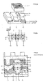
- FIG. 1 shows the cell construction
- FIG. 1b shows the cell layout
- FIG. 1c shows the cross section
- FIG. 2a shows the cell construction
- FIG. 2b shows the cell layout
- FIG. 2c the cross section
- CMOS wells are formed in a p-doped silicon substrate with a LOGOS process field isolation areas and active areas and then LDD-MOS transistors, consisting of isolated polysilicon word lines 12 with silicon dioxide cover insulation, lateral insulation spacers and source 7 and drain regions 9.
- a 400 nm thick, rounded lower insulation layer 11 is then applied and structured, as a result of which source contact windows 8 are opened in the memory matrix.
- the bit line is then generated and connected by deposition, doping and structuring of a polycid layer.
- a 650 nm thick top layer 13, rounded by means of RTA, is applied (FIG. 4a) and with a RIE process via a resist mask in the drain regions 9 of the n-LDD-MOS transistors of the Spelcher matrix, steep-sided drain contact window 10 with a minimal contact window width of 1.0 ⁇ m was introduced into the upper insulation layer 13, the etching process being stopped by its selectivity with respect to the bit line material on the bit line surface.
- Another RIE process cuts through the bit line 6 exposed in the drain contact window 10, the lower insulation layer 11 being etched to a remaining thickness of 200 nm.
- a 20 nm thick, phosphorus-doped polysilicon layer is deposited. Then a 200 nm thick tungsten CVD layer conformally covering the steep flanks of the drain contact window 10 is applied (FIG. 4b) and removed again from all horizontal surfaces by a subsequent anisotropic RIE process. However, on the steep flanks of the drain contact window 10, the double layer consisting of tungsten and polysilicon remains in the form of a conductive ring 16. The conductive ring 16 contacts and closes the bit line 6 broken through the drain contact window etching process except for that in the center of the conductive Ring's remaining drain contact window 10 again.
- the upper insulation layer 13 is removed over a large area and, in the region of the remaining drain contact window 10, the lower insulation layer 11 is also removed by approximately 50 nm.
- a thin insulation layer 20 in the form of a 50 nm thick silicon nitride layer is deposited by means of an LPCVD process and removed from the horizontal surfaces by an anisotropic RIE etching process, the silicon nitride layer 20 remaining on the inner horizontal wall surface of the conductive ring 16 obtained with unattenuated thickness (Fig. 4c).
- the exposed upper cover surface of the conductive ring 16 is then isotropically and selectively etched down to a level of approximately 200 nm above the bit line surface, the silicon nitride layer 20 on the inner vertical wall surface of the conductive ring 16 being completely retained.
- a 140 nm thick silicon layer is then deposited using an LPCVD process (FIG. 4d) and then removed again on all horizontal surfaces by an anisotropic RIE process.
- the drain contact window 10 remaining in the center of the conductive ring 16 is subsequently opened up to the substrate surface.
- the conductive ring 16 is thus covered on its upper cover surface and its inner vertical wall surface by an insulation jacket 15, which is formed from two mask-free structured silicon nitride layers.
- n-conductive polysilicon layer becomes the lowest bottom plate layer 2a, which contacts the drain region 9 and the drain contact window 10 remaining in the center of the conductive ring 16 and its insulation jacket 15 a conductive stamp 14 completely filled out, deposited.
- auxiliary insulator layer 17 is applied (FIG. 4e; FIG. 3b) and a steep-sided breakthrough with a width of 1 is applied via a lacquer mask with an anisotropic selective RIE process, which is stopped on the bottom base plate layer 2A , 6 ⁇ m are introduced into the auxiliary insulator layer 17.
- an n-conducting polysilicon layer with a thickness of 175 nm is deposited as the first conductive lamella layer, then a first thin auxiliary insulation layer 18 with a thickness of 180 nm is applied (FIG.
- the layer stack of all lamella layers lying on the surface of the thick auxiliary insulation layer 17 is then removed using an RIE process, the surfaces of the thick auxiliary insulation layer 17 and the thin auxiliary insulation layers 18 remaining in the steep-sided opening being exposed and the upper ends of the layers being arranged vertically in the opening Polysilicon lamellae 3 are separated from one another (FIG. 3f).
- the polysilicon lamellae 3 which are vertically free in the area of the previous steep-sided opening, are removed vertically by the anisotropic RIE method by the thickness of the lowest base plate layer 2A, the RIE -Procedure is stopped on the upper insulation layer 13.
- the self-aligning etching of the bottom floor slab layer 2A takes place in the area outside the previous steep-sided opening and thus the separation of the storage electrodes 1 of adjacent storage cells, the conductive floor slab 2 connecting the conductive lamellae horizontally, that of the bottom floor slab layer 2A and horizontal parts of the polysilicon lamella layers is thinned by the thickness of the lowermost base plate layer, but is not cut through (FIG. 3h).
- an ONO storage dielectric 4 with a silicon dioxide equivalent thickness of 3 nm is produced from a 3 nm thick polysilicon layer, a 10 nm thick LPCVD silicon nitride layer and a reoxidation of the silicon nitride layer.
- n-doped polysilicon layer is then deposited and structured as a cell plate 5 with a thickness of 150 nm, which completely fills the spaces between the polysilicon fins 3.
Landscapes
- Engineering & Computer Science (AREA)
- Manufacturing & Machinery (AREA)
- Semiconductor Memories (AREA)
- Dram (AREA)
Abstract
Die Erfindung betrifft eine Ein-Transistor-Speicherzellenanordnung und ein Verfahren zu deren Herstellung, insbesondere für höchstintegrierte dynamische Halbleiterspeicher.The invention relates to a one-transistor memory cell arrangement and a method for its production, in particular for highly integrated dynamic semiconductor memories.
Die erfindungsgemäße Speicherzellenanordnung ist im wesentlichen dadurch gekennzeichnet, daß die Speicherelektrode aus senkrecht zur Substratoberfläche, auf einer gemeinsamen leitenden Bodenplatte angeordneten leitenden Lamellen besteht, daß ein Speicherdielektrikum die Speicherelektrode mit Ausnahme der Bodenplattenunterseite bedeckt, daß eine Zellplatte die Speicherelektrode verzahnt umschließt, wobei die Abstände zwischen den benachbarten Lamellen vollständig ausgefüllt sind und die an die äußerste Lamelle grenzenden mit Speicherdielektrikum bedeckten Bereiche der Bodenplatte und der Speicherzelle ebenfalls mit der Zellplatte bedeckt sind und daß an entwurfsbedingt notwendigen Kontaktstellen in der Zellplatte Durchbrüche angeordnet sind.
Description
Die Erfindung betrifft eine Ein-Transistor-Speicherzellenanordnung und ein Verfahren zu deren Herstellung, insbesondere für höchstintegrierte dynamische Halbleiterspeicher.The invention relates to a one-transistor memory cell arrangement and a method for its production, in particular for highly integrated dynamic semiconductor memories.
Die Grundstruktur für dynamische Halbleiterspeicher nach dem Prinzip der Ein-Transistor-Zelle besteht aus einem MOS-Auswahltransistor und einem Speicherkondensator mit einer Speicherkapazität von 30 bis 50 fF, der die logische Information als gespeicherte Ladung enthält. Der Auswahltransistor ist über eine Wortleitung ansteuerbar. Sein Draingebiet ist mit einer Elektrode des Speicherkondensators verbunden, während sein Sourcegebiet nach außen über eine Bitleitung mit in Bitleitungsrichtung liegenden Sourcegebieten weiterer Speicherzellen verbunden ist. In dRAM-Speichern bis 1 Mbit werden die Speicherkondensatoren in der Regel durch einen hochdotierten Substratflächenabschnitt, einem darüberliegenden Speicherdielektrikum (in der Regel Siliziumdioxid) und einer Polysiliziumzellplatte als planare Anordnung ausgebildet.The basic structure for dynamic semiconductor memories based on the principle of the one-transistor cell consists of a MOS selection transistor and a storage capacitor with a storage capacity of 30 to 50 fF, which contains the logical information as a stored charge. The selection transistor can be controlled via a word line. Its drain region is connected to an electrode of the storage capacitor, while its source region is connected to the outside via a bit line with source regions of further memory cells lying in the bit line direction. In dRAM memories up to 1 Mbit, the storage capacitors are generally formed as a planar arrangement by a highly doped substrate surface section, an overlying storage dielectric (usually silicon dioxide) and a polysilicon cell plate.
Um die Integrationsdicte zu erhöhen, werden Zellkonzepte mit einem dreidimensionalen Speicherkondensator als Trench- oder Stapelkondensator (STC) oder in Mischvarianten realisiert. Das STC-Zellkonzept zeichnet sich gegenüber dem Trenchzellkonzept vorteilhaft durch eine weitgehende elektrische Entkopplung der Speicherkapazität vom aktiven Silizium aus. Dadurch bleibt das aktive Silizium in der Regel bis auf die Drainkontaktierung einer unteren Speicherelektrode morphologisch ungestört. Infolgedessen werden die für die Trenchzellenkonzepte typischen Substratdefekte beziehungsweise die zur Beseitigung dieser Defekte in der Regel notwendigen technologischen Maßnahmen und die laterale Wechselwirkung benachbarter Speicherkapazitäten über das Siliziumsubstrat prinzipiell vermieden sowie eine natürliche, ohne gesonderte Maßnahmen vorhandene, hohe ALPHA-Immunität gewährleistet. Bei der konventionellen STC-Speicherzelle besteht der Speicherkondensator aus zwei übereinanderliegenden dotierten Polysiliziumschichten mit dazwischenliegendem Speicherdielektrikum. Die untere Polysiliziumschicht fungiert dabei als Speicherelektrode und ist mit dem Draingebiet des Auswahltransistors verbunden. Die obere Polysiliziumschicht fungiert als gemeinsame Zellplatte einer Speichermatrix. Der Elektrodenstapel überlappt das Gate des Auswahltransistors (vgl. Koyanagi, IEDM Tech. Dig. 1978, S. 348-351).In order to increase the integration density, cell concepts are implemented with a three-dimensional storage capacitor as a trench or stack capacitor (STC) or in mixed versions. The STC cell concept is distinguished from the trench cell concept by the fact that the storage capacity is largely electrically decoupled from the active silicon. As a result, the active silicon generally remains morphologically undisturbed except for the contacting of a lower storage electrode. As a result, the substrate defects typical of the trench cell concepts or the technological measures generally required to eliminate these defects and the lateral interaction of adjacent storage capacities via the silicon substrate avoided in principle and guaranteed a natural, high ALPHA immunity without special measures. In the conventional STC memory cell, the storage capacitor consists of two stacked doped polysilicon layers with a storage dielectric in between. The lower polysilicon layer acts as a storage electrode and is connected to the drain region of the selection transistor. The upper polysilicon layer acts as a common cell plate of a memory matrix. The electrode stack overlaps the gate of the selection transistor (cf. Koyanagi, IEDM Tech. Dig. 1978, pp. 348-351).
Aus EP-PS 0191612 ist eine verbesserte STC-Variante bekannt, bei der die Zellplatte den Rand der Speicherelektrode überlappt, wodurch deren Seitenflanke als Flächenbeitrag für eine höhere Speicherkapazität gewonnen wird. Durch die gleichzeitige Auffüllung der Bitleitungskontaktfenster mit der Herstellung der Speicherelektrode wird außerdem das Problem des Bitleitungsabrisses an den Flanken des Bitleitungskontaktfensters gelöst. Diese Vorteile können bekannterweise (EP-PS 0263941) durch Erhöhung der Dicke der Speicherelektrode verstärkt werden.An improved STC variant is known from EP-PS 0191612, in which the cell plate overlaps the edge of the storage electrode, as a result of which its side flank is obtained as an area contribution for a higher storage capacity. The simultaneous filling of the bit line contact window with the production of the storage electrode also solves the problem of the bit line break on the flanks of the bit line contact window. As is known (EP-PS 0263941), these advantages can be increased by increasing the thickness of the storage electrode.
Weiterhin ist ein Verfahren (EP-PS 0223616) bekannt, bei dem durch Vertiefung des Drainkontaktfensters in das Siliziumsubstrat hinein mittels eines RIE-Prozesses ein Graben erzeugt wird, der durch seine Topologie nach Abscheidung der Speicherelektrodenschicht ebenfalls zu einer Vergrößerung der kapazitiven Fläche beiträgt.Furthermore, a method (EP-PS 0223616) is known in which a trench is produced by deepening the drain contact window into the silicon substrate by means of an RIE process, the topology of which also contributes to an increase in the capacitive area after the storage electrode layer has been deposited.
Eine noch größere Speicherkapazität ist durch Kombination der Reliefbeiträge einer dicken Speicherelektrode und eines Grabens im Drainkontaktfenster erreichbar (IEDM Tech. Dig., 1988, S. 600-603).An even larger storage capacity can be achieved by combining the relief contributions of a thick storage electrode and a trench in the drain contact window (IEDM Tech. Dig., 1988, pp. 600-603).
Durch die aufgeführten dreidimensionalen SIC-Varianten wird ein topologisches Relief erzeugt, das abrißfreie Bitleitungskontaktierung erschwert, wenn die Bitleitung über den Speicherkondensator geführt wird. Zur Beseitigung dieses Nachteiles ist aus IEDM Tech. Dig. 1988, S. 596-599 eine Lösung bekannt, in welcher die Bitleitung unter der Speicherkapazität durchgeführt wird. Bei diesem DASH-STC-Konzept erfolgt die Bitleitungsherstellung nach der Fertigstellung des Auswahltransistors derart, daß die Bitleitung seitlich am späteren Drainkontaktfenster für die Speicherelektrode vorbeigeführt wird. Damit ist die prinzipielle Möglichkeit erschlossen, den STG-Komplex vertikal zu vergrößern, ohne daß Probleme bei der Bitleitungsstrukturierung und -kontaktierung auftreten.The three-dimensional SIC variants listed produce a topological relief which makes it difficult to break off bit line contact when the bit line is passed over the storage capacitor. To overcome this disadvantage, IEDM Tech. Dig. 1988, S. 596-599 a solution is known in which the bit line is carried out under the storage capacity. In this DASH-STC concept, the bit line is produced after the selection transistor has been completed in such a way that the bit line is guided laterally past the later drain contact window for the storage electrode. This opens up the basic possibility of vertically enlarging the STG complex without problems with bit line structuring and contacting.
Desweiteren ist aus EP-PS 0295709 ein STC-Zellenkonzept ("fin-Typ") bekannt, bei dem die Speicherelektrode aus einem untereinander kontaktierten Mehrfach-Polysiliziumstapel besteht, der den Auswahltransistor überlappt. Diese Polysiliziumfinnen werden allseitig vom Speicherdielektrikum und einer gemeinsamen Polysilizium-Zellplatte umschlossen.Furthermore, an STC cell concept ("fin type") is known from EP-PS 0295709, in which the storage electrode consists of a mutually contacted multiple polysilicon stack which overlaps the selection transistor. These polysilicon fins are enclosed on all sides by the storage dielectric and a common polysilicon cell plate.
Ema u. a. beschreiben in IEDM Tech. Dig. 1988, S.592-595 beide Möglichkeiten der Bitleitungsführung unter- und oberhalb einer Speicherkapazität vom "fin-Typ".Ema u. a. describe in IEDM Tech. Dig. 1988, p.592-595 both possibilities of the bit line routing below and above a storage capacity of the "fin type".
Für Speicher größer gleich 16 MdRAM muß die Bitleitung unter dem STC-Komplex angeordnet sein. Derartig komplex strukturierte Speicherelektroden sind fertigungstechnisch schwer beherrschbar (vgl. IEDM Tech. Dig. 1989, S. 31-34). Außerdem beschreiben Inoue u. a. ebenda mit einem SSC-Zellenkonzept für 64 MdRAM bzw. 256 MdRAM eine Lösung, bei der die Bitleitung unter dem STC-Komplex angeordnet ist und sich Speicherelektroden vom "fin-Typ" bis in benachbarte Zellengebiete hinein wechselseitig überlappen.For memories greater than or equal to 16 MdRAM, the bit line must be arranged under the STC complex. Such complexly structured storage electrodes are difficult to control in terms of production technology (cf. IEDM Tech. Dig. 1989, pp. 31-34). Inoue et al. a. ibid with an SSC cell concept for 64 MdRAM or 256 MdRAM, a solution in which the bit line is arranged under the STC complex and storage electrodes of the "fin type" overlap each other into neighboring cell areas.
Nachteilig an beiden letztgenannten Lösungen, gleichgültig ob die den Speicherelektrodenstapel bildenden Polysiliziumfinnen nur das eigene Zellengebiet oder auch die benachbarten Zellengebiete überlappen, ist, daß während der Herstellung eine Bearbeitungsphase auftritt, bei der die horizontal übereinander angeordneten Polysiliziumfinnen freitragend mehreren Verfahrensschritten ausgesetzt sind. Diese Verfahrensschritte, wie Naßätz- und Reinigungsschritte, Oxydation, Isolator- und Polysilizium-CVD-Abscheidungen, stellen für diese empfindlichen, freitragenden Speicherelektrodenkonfigurationen beträchtliche mechanische, chemische und thermische Beanspruchungen dar.A disadvantage of the latter two solutions, irrespective of whether the polysilicon fins forming the storage electrode stack overlap only the own cell area or also the neighboring cell areas, is that during processing a processing phase occurs in which the horizontally arranged polysilicon fins are exposed to several process steps in a cantilever manner are. These process steps, such as wet etching and cleaning steps, oxidation, insulator and polysilicon CVD deposition, represent significant mechanical, chemical, and thermal stresses for these sensitive, cantilevered storage electrode configurations.
Bedingt durch das Herstellungsverfahren zur Erzeugung der Polysiliziumfinnen und der Forderung, eine große speicherwirksame Strukturoberfläche zu erzielen, sind die Finnen vorzugsweise sehr dünn (kleiner gleich 100 nm) bei zugleich großem Länge- zu Dicke-Verhältnis und nur linienhaft mit den anderen Finnen derselben Speicherelektrode bzw. dem einkristallinen Siliziumsubstrat verwachsen. Dadurch ist die Stabilität solcher freitragenden Speicherelektroden gering und infolgedessen die Ausbeute bei der Herstellung der Speicherzelle negativ beeinflußt.Due to the manufacturing process for the production of the polysilicon fins and the requirement to achieve a large memory - effective structure surface, the fins are preferably very thin (less than or equal to 100 nm) with a large length to thickness ratio and only in line with the other fins of the same storage electrode or grown on the single-crystalline silicon substrate. As a result, the stability of such self-supporting storage electrodes is low and, as a result, the yield in the production of the storage cell is adversely affected.
Weiterhin ist nachteilig, daß die zwischen den Polysiliziumfinnen liegenden, langen und schmalen Zwischenräume parallel zur Siliziumsubstratoberfläche liegen und zum Beispiel durch Naßätz- und Reinigungsprozesse nur über senkrecht dazu liegende, schachtförmige Kanäle erreichbar sind. Dadurch ergeben sich insbesondere bei der Oberflächenbehandlung der freitragenden Polysiliziumfinnen durch Naßätz- und Reinigungsprozesse, aber auch für die folgenden CVD-Beschichtungsprozesse für den Speicherisolator und die Polysilizium-Zellplatte ungünstige Antransport-, Abtransport- und Austauschbedingungen für flüssige und gasförmige Medien in den Mikrobereichen der Speicherelektrodenkonfiguration. Diese Prozesse müssen jedoch die notwendige hohe Ausgangsqualität der Speicherelektrodenoberfläche bzw. die hohe Qualität des in der Regel sehr dünnen (kleiner gleich 10 nm Siliziumdioxid-Äquivalent), durchschlagsfesten (größer gleich 6 MV/cm) Speicherdielektrikums und der Zellplatte mit hoher Ausbeute, reproduzierbar sichern.A further disadvantage is that the long and narrow spaces between the polysilicon fins lie parallel to the silicon substrate surface and can only be reached, for example, by wet etching and cleaning processes via shaft-shaped channels lying perpendicular to it. This results in unfavorable transport, removal and exchange conditions for liquid and gaseous media in the micro areas of the storage electrode configuration, in particular for the surface treatment of the self-supporting polysilicon fins by wet etching and cleaning processes, but also for the subsequent CVD coating processes for the storage insulator and the polysilicon cell plate . However, these processes must reproducibly ensure the necessary high output quality of the storage electrode surface or the high quality of the generally very thin (less than or equal to 10 nm silicon dioxide equivalent), dielectric strength (greater than or equal to 6 MV / cm) storage dielectric and the cell plate with high yield .
Weiterhin ist nachteilig, daß die mindestens ab größer gleich 64 MdRAM notwendige Anordnung des Speicherelektrodenkomplexes über der Bitleitung dadurch gelöst wird, daß die Bitleitung am Drainkontaktfenster für den späteren Anschluß der unteren Speicherelektrode seitlich vorbeigeführt wird, wobei zwischen der Bitleitung und dem Drainkontaktfenster ein zusätzlicher justagebedingter Sicherheitsabstand einzuhalten ist. Dadurch ergibt sich an dieser Stelle eine nicht zu unterschreitende Breite B min der Speicherzelle (B min = Bitleitungsbreite + Drainkontaktfensterbreite + zweimal den justagebedingten Sicherheitsabstand).Another disadvantage is that the arrangement of the storage electrode complex, which is at least greater than or equal to 64 MdRAM, is necessary Is solved over the bit line in that the bit line is guided laterally past the drain contact window for the later connection of the lower storage electrode, an additional adjustment-related safety distance between the bit line and the drain contact window being maintained. This results in a width B min of the memory cell which is not to be undercut (B min = bit line width + drain contact window width + twice the adjustment-related safety distance).
Ziel der Erfindung sind eine Ein-Transistor-Speicherzellenanordnung für dynamische Halbleiterspeicher und ein Verfahren zu deren Herstellung, die die Qualität und Stabilität der Speicherelektroden des STC-Komplexes mit hoher Reproduzierbarkeit wesentlich verbessern, die Ausbeute des Herstellungsprozesses erhöhen und eine Steigerung der Packungsdichte gewährleisten.The aim of the invention is a one-transistor memory cell arrangement for dynamic semiconductor memories and a method for their production, which significantly improve the quality and stability of the storage electrodes of the STC complex with high reproducibility, increase the yield of the production process and ensure an increase in the packing density.
Der Erfindung liegt die Aufgabe zugrunde, eine Ein-Transistor-Speicherzelllenanordnung für dynamische Halbleiterspeicher und ein Verfahren zu deren Herstellung zu schaffen, welche für flüssige und gasförmige Medien bei der Durchführung von Naßätz- und Reinigungsprozessen sowie von Beschichtungsverfahren, insbesondere bei der Ausbildung des STC-Komplexes, günstige Bedingungen gewährleisten und einen justagebedingten Sicherheitsabstand bei Anordnung des STC-Komplexes oberhalb der Bitleitung vermeiden.The object of the invention is to create a one-transistor memory cell arrangement for dynamic semiconductor memories and a method for their production, which are suitable for liquid and gaseous media when carrying out wet etching and cleaning processes and also coating methods, in particular when designing the STC Ensure complex, favorable conditions and avoid an adjustment-related safety distance when the STC complex is arranged above the bit line.
Erfindungsgemäß wird die Aufgabe durch eine Ein-Transistor-Speicherzelle für höchstintegrierte dynamische Halbleiterspeicher, bestehend aus Feldisolationsgebieten und aktiven Oberflächenbereichen eines einkristallinen Substrates, in denen ein MOS-Feldeffekttransistor mit einer allseitig isolierten Wortleitung und einem Source- und und Draingebiet integriert ist, sowie einem über der Wortleitung angeordneten und das Gebiet der Speicherzelle weitgehend bedeckenden Stapelkondensator (STC)-Komplex, welcher mit seiner Speicherelektrode an das Draingebiet angeschlossen ist und dessen obere Elektrode als Zellplatte aller Speicherzellen eines Speichermatrixblockes ausgebildet ist und einer mit dem Sourcegebiet kontaktierten Bitleitung, dadurch gelöst, daß die Speicherelektrode aus senkrecht zur Substratoberfläche auf einer gemeinsamen, leitenden Bodenplatte angeordneten leitenden Lamellen besteht, von denen jede im Speicherzellenlayout ein in sich zurücklaufendes und geschlossenes Band, dessen Breite der Wandstärke der Lamellen entspricht, darstellt, daß jede der Lamellen beginnend mit einer äußersten Lamelle, die innerhalb der Speicherzelle angeordnet ist, eine jeweils kleinere umschließt, wobei entlang des Lamellenumfanges der Wand- zu Wand-Abstand benachbarter Lamellen konstant ist und ungefähr der Lamellenwandstärke entspricht, daß die inneren Wandflächen der innersten im Zentrum des Stapelkondensatorkomplexes angeordneten Lamelle sich ganzflächig berühren, daß ein Speicherdielektrikum die Speicherelektrode mit Ausnahme der Bodenplattenunterseite bedeckt, daß eine Zellplatte die Speicherelektrode verzahnt umschließt, wobei die Abstände zwischen den benachbarten Lamellen vollständig ausgefüllt sind und die an die äußerste Lamelle grenzenden mit Speicherdielektrikum bedeckten Bereiche der Bodenplatte und der Speicherzelle ebenfalls mit der Zellplatte bedeckt sind und daß an entwurfsbedingt notwendigen Kontaktstellen in der Zellplatte Durchbrüche angeordnet sind.According to the invention, the object is achieved by a one-transistor memory cell for highly integrated dynamic semiconductor memories, consisting of field isolation regions and active surface areas of a single-crystalline substrate, in which a MOS field effect transistor with an all-round insulated word line and a source and drain region is integrated, as well as one above arranged in the word line and largely covering the area of the memory cell stack capacitor (STC) complex, which is connected with its storage electrode to the drain area and its upper electrode as Cell plate of all memory cells of a memory matrix block is formed and a bit line contacted with the source region, solved in that the memory electrode consists of conductive lamellae arranged perpendicular to the substrate surface on a common, conductive base plate, each of which in the memory cell layout has a self-contained and closed band, the Width corresponds to the wall thickness of the slats, represents that each of the slats, starting with an outermost slat, which is arranged within the storage cell, encloses a smaller one, with the wall-to-wall distance of adjacent slats being constant along the slat circumference and approximately the slat wall thickness corresponds to the fact that the inner wall surfaces of the innermost lamella arranged in the center of the stacked capacitor complex touch the whole area, that a storage dielectric covers the storage electrode with the exception of the bottom plate underside, that a Z Ellplatte encloses the storage electrode toothed, the distances between the adjacent lamellae are completely filled and the areas of the base plate and the storage cell covered with storage dielectric bordering on the outermost lamella are also covered with the cell plate and that openings are arranged in the cell plate at design-related necessary contact points .
In einer Ausgestaltung der Erfindung entspricht die Bodenplatte im Speicherzellenlayout exakt der Fläche, die vom Umfang der äußersten Lamelle eingeschlossen wird. In einer weiteren Ausgestaltung ist die Speicherzellenanordnung derart gestaltet, daß die Bodenplatte aus mehreren leitenden Schichten besteht, wobei die Schichtdicke einer untersten leitenden Bodenplattenschicht kleiner gleich der Wandstärke der Lamellen ist und die Bodenplattenfläche zumindest der Fläche entspricht, die vom Umfang der äußersten Lamelle eingeschlossen ist, daß auf der untersten leitenden Bodenplattenschicht eine zweite leitende Schicht angeordnet ist, deren Schichtdicke der Wandstärke der äußersten Lamelle entspricht und deren Fläche der vom Umfang der äußersten Lamelle eingeschlossenen Fläche exakt entspricht, daß auf der zweiten leitenden Schicht eine dritte leitende Schicht angeordnet ist, deren Schichtdicke der Wandstärke der nächstinneren Lamelle entspricht und deren Fläche der vom Umfang der nächstinneren Lamelle eingeschlossenen Fläche exakt entspricht und daß weitere leitende Schichten analog zu den vorhergehend genannten Schichten angeordnet sind.In one embodiment of the invention, the base plate in the memory cell layout corresponds exactly to the area enclosed by the periphery of the outermost lamella. In a further embodiment, the memory cell arrangement is designed in such a way that the base plate consists of a plurality of conductive layers, the layer thickness of a lowermost conductive base plate layer being less than or equal to the wall thickness of the slats, and the base plate surface corresponding at least to the area enclosed by the periphery of the outermost slat, that a second conductive layer is arranged on the lowermost conductive base plate layer, the layer thickness of which corresponds to the wall thickness of the outermost lamella and the area of which corresponds to the circumference of the outermost lamella enclosed area corresponds exactly to the fact that a third conductive layer is arranged on the second conductive layer, the layer thickness of which corresponds to the wall thickness of the next inner lamella and whose area corresponds exactly to the area enclosed by the circumference of the next inner lamella, and that further conductive layers are analogous to the layers mentioned above are arranged.
In einer Ausgestaltung der Erfindung ist die Speicherzellenanordnung dadurch gekennzeichnet, daß die Lamellen unabhängig vom Relief der Bodenplatte mit der sie kontaktiert sind und unabhängig vom Relief der unter der Bodenplatte angeordneten Speicherzellenelemente, in einheitlicher Höhe über dem Niveau der Substratoberfläche enden.In one embodiment of the invention, the memory cell arrangement is characterized in that the lamellae end at a uniform height above the level of the substrate surface, regardless of the relief of the base plate with which they are contacted and regardless of the relief of the memory cell elements arranged under the base plate.
Eine weitere Ausgestaltung der Speicherzellenanordnung ist dadurch gekennzeichnet, daß eine Bitleitung auf dem isolierten Stapelkondensatorkomplex angeordnet ist, wobei der im Sourcekontaktfenster liegende Teil der Bitleitung stempelartig und gegenüber der Oberseite des Stapelkondensatorkomplexes planarisiert ausgebildet ist und daß die Drainkontaktierung der Speicherelektrode durch direkten Kontakt der Bodenplatte mit dem Draingebiet in einem Drainkontaktfenster einer unteren Isolatorschicht, die auf den isolierten Wortleitungen und über den restlichen Speicherzellenbereichen mit Ausnahme der Kontaktfenster der Source- und Draingebiete angeordnet, erfolgt.A further embodiment of the memory cell arrangement is characterized in that a bit line is arranged on the insulated stack capacitor complex, the part of the bit line lying in the source contact window being stamp-like and planarized with respect to the top of the stack capacitor complex, and in that the drain contacting of the memory electrode by direct contact of the base plate with the Drain area in a drain contact window of a lower insulator layer, which is arranged on the isolated word lines and over the remaining memory cell regions with the exception of the contact windows of the source and drain regions.
Die Speicherzellenanordnung ist in einer weiteren Ausgestaltung der Erfindung dadurch gekennzeichnet, daß die mit einer oberen Isolationsschicht bedeckte Bitleitung unterhalb des Stapelkondensatorkomplexes angeordnet ist, wobei die Bitleitung auf der unteren Isolationsschicht oberhalb der Wortleitungsisolation angeordnet ist und die untere Isolationsschicht alle Bereiche der Speicherzelle, außer den Source- und Drainkontaktfensterbereich, bedeckt, daß die Bitleitung im Sourcekontakfenster das Sourcegebiet kontaktiert und daß ein isolierter leitender Stempel, der das Draingebiet im Drainkontaktfenster kontaktiert, die untere Isolationsschicht, die Bitleitung und die obere Isolationsschicht durchstößt und die Unterseite der Bodenplatte kontaktiert.In a further embodiment of the invention, the memory cell arrangement is characterized in that the bit line covered with an upper insulation layer is arranged below the stack capacitor complex, the bit line being arranged on the lower insulation layer above the word line insulation and the lower insulation layer all regions of the memory cell, except the source and drain contact window area, covers that the bit line in the source contact window contacts the source area and that an insulated conductive Stamp that contacts the drain area in the drain contact window, penetrates the lower insulation layer, the bit line and the upper insulation layer and contacts the underside of the base plate.
In einer Ausgestaltung dieser erfindungsgemäßen Anordnung ist die vertikale Oberfläche des Stempels von einem Isolationsmantel mit konstanter Dicke selbstjustierend bedeckt.In an embodiment of this arrangement according to the invention, the vertical surface of the stamp is covered by an insulating jacket with a constant thickness in a self-adjusting manner.
Desweiteren ist diese Speicherzellenanordnung in einer Ausgestaltung dadurch gekennzeichnet, daß die Bitleitung bei einem Stempeldurchmesser vom annähernd der Bitleitungsbreite an der Durchstoßstelle durch einen leitenden Ring, der den isolierten Stempel mit konstanter Dicke selbstjustierend umschließt, ergänzt ist, wobei der leitende Ring in seiner Höhe mindestens der Dicke der Bitleitung entspricht und gegenüber dem Draingebiet, der Wortleitung und der Bodenplatte elektrisch isoliert ist.Furthermore, this memory cell arrangement is characterized in one embodiment in that the bit line is supplemented with a stamp diameter of approximately the bit line width at the point of penetration by a conductive ring which surrounds the insulated stamp with a constant thickness, the height of the conductive ring being at least that Corresponds to the thickness of the bit line and is electrically insulated from the drain region, the word line and the base plate.
Erfindungsgemäß wird die Aufgabe weiterhin durch ein Verfahren zur Herstellung einer Ein-Transistor-Speicherzellenanordnung, bei dem in einem einkristallinen Substrat n-leitende und p-leitende Bereiche, Feldisolationsgebiete und nachfolgend MOS-Feldeffekttransistoren mit allseitig isolierten Wortleitungen und Source- und Draingebiete, eine unterste leitende Schicht einer Speicherelektrode, welche den Kontakt eines Stapelkondensators zum darunterliegenden Draingebiet der Speicherzelle erzeugt, der in eine Speichermatrix integrierte Stapelkondensatorkomplex und die mit dem Sourcegebiet der Speicherzelle kontaktierte Bitleitung ausgebildet werden und abschließend an Kontaktstellen Durchbrüche in die Zellplatte des Stapelkondensatorkomplexes geätzt werden, dadurch gelöst, daß nach Abscheidung einer untersten leitenden Schicht der Bodenplatte eine dicke Hilfsisolationsschicht planarisiert abgeschieden wird, daß im Anschluß in die dicke Hilfsisolationsschicht ein steilflankiger Durchbruch bis auf die unterste leitende Schicht ausgebildet wird, daß nachfolgend beginnend und endend mit einer Abscheidung einer leitenden Lamellenschicht in abwechselnder Folge eine leitende Lamellenschicht und danach eine dünne Hilfsisolationsschicht abgeschieden werden, wobei die doppelte Summe aller leitenden Lamellen- und Hilfsisolationsschichtdicken dem kürzesten Abstand sich gegenüberliegender Wandflächen des steilflankigen Durchbruchs in der dicken Hilfsisolationsschicht entspricht, und zumindest nach jeder Abscheidung einer dünnen Hilfsisolationsschicht ein anisotroper RIE-Prozeß durchgeführt wird, wobei auf der Oberfläche der dicken Hilfsisolationsschicht und auf der Bodenfläche im Durchbruch zumindest die zuletzt abgeschiedene Schicht abgeätzt wird, während die zuletzt abgeschiedene und alle zuvor abgeschiedenen Schichten an den senkrechten Wänden des Durchbruchs verbleiben und eine Lamellenstruktur bilden, daß nach der Abscheidung der letzten leitenden Lamellenschicht mittels eines RIE-Prozesses die Oberfläche der dicken Hilfsisolationsschicht von der letzten Lamellenschicht und darunterliegend verbliebenen Lamellenschichten freigeätzt wird, wodurch die oberen Enden der freigeätzten Lamellen voneinander getrennt werden, daß anschließend mittels eines isotropen, gegenüber den Lamellen und der Bodenplatte selektiven Ätzverfahrens die zwischen den Lamellen liegenden dünnen Hilfsisolationsschichten und zugleich die Reste der dicken Hilfsisolationsschicht im gesamten Speicherzellengebiet entfernt werden, daß im Anschluß daran die Bodenplatte der Speicherzelle strukturiert wird, wodurch die aus der Bodenplatte und den Lamellen bestehende Speicherelektrode von benachbarten Speicherelektroden angrenzender Speicherzellen elektrisch getrennt wird, daß nachfolgend durch ein Ätz- und Reinigungsverfahren die Lamellenoberflächen und die Bodenplattenoberfläche geglättet und gereinigt werden, daß anschließend ein Speicherdielektrikum ausgebildet wird, welches die Speicherelektrodenoberfläche vollständig bedeckt, daß danach eine leitende Schicht abgeschieden wird, die die Zwischenräume benachbarter Lamellen vollständig ausfüllt, die Lamellen verzahnt umschließt und eine Zellplatte bildet und daß anschließend eine die Zellplatte planarisierende Deckisolationsschicht ausgebildet wird.According to the invention, the object is further achieved by a method for producing a one-transistor memory cell arrangement in which n-type and p-type regions, field isolation regions and subsequently MOS field effect transistors with word lines and source and drain regions insulated on all sides in a single-crystal substrate conductive layer of a storage electrode, which produces the contact of a stacked capacitor to the drain region of the memory cell underneath, the stacked capacitor complex integrated in a memory matrix and the bit line contacted with the source region of the memory cell, and finally openings in the cell plate of the stacked capacitor complex are etched at contact points, that after the deposition of a lowermost conductive layer of the base plate, a thick auxiliary insulation layer is deposited in a planarized manner, that a steep-sided Durc Breakage is formed down to the lowest conductive layer, that subsequently begins and ends with a deposition of a conductive lamella layer alternately a conductive lamella layer and then a thin auxiliary insulation layer are deposited, the double sum of all conductive lamella and auxiliary insulation layer thicknesses corresponding to the shortest distance between opposing wall surfaces of the steep-sided opening in the thick auxiliary insulation layer, and an anisotropic RIE at least after each deposition of a thin auxiliary insulation layer -Process is carried out, on the surface of the thick auxiliary insulation layer and on the bottom surface in the opening at least the last deposited layer is etched, while the last deposited and all previously deposited layers remain on the vertical walls of the opening and form a lamellar structure that after Deposition of the last conductive lamella layer by means of an RIE process the surface of the thick auxiliary insulation layer from the last lamella layer and the lame remaining underneath Oil layers is etched free, whereby the upper ends of the etched lamellae are separated from each other, that the thin auxiliary insulation layers lying between the lamellae and at the same time the remainders of the thick auxiliary insulation layer in the entire memory cell area are subsequently removed by means of an isotropic etching process which is selective with respect to the lamellae and the base plate the base plate of the memory cell is then structured, whereby the memory electrode consisting of the base plate and the lamellae is electrically separated from adjacent memory electrodes of adjacent memory cells, that the lamella surfaces and the base plate surface are subsequently smoothed and cleaned by an etching and cleaning process, and then a Storage dielectric is formed, which completely covers the storage electrode surface, that a conductive layer is then deposited, which use the spaces neighboring fins completely filled, the lamella encloses toothed and forms a cell plate and that a cover insulation layer planarizing the cell plate is then formed.
In einer Ausgestaltung der Erfindung ist das Verfahren dadurch gekennzeichnet, daß innerhalb der abwechselnden Folge der Abscheidung der leitenden Lamellenschichten und der dünnen Hilfsisolationsschichten die Dicke der Lamellenschichten zumindest der Dicke der untersten Schicht der Bodenplatte entspricht und nach der Abscheidung jeder dünnen Hilfsisolationsschicht ein anisotroper RIE-Ätzprozeß durchgeführt wird, der auf der Oberfläche der dicken Hilfsisolationsschicht liegenden Schichtstapel aller leitenden Lamellenschichten entfernt, wodurch die oberen Enden der senkrecht zur Substratoberfläche stehenden Lamellen voneinander getrennt werden, daß nach der isotropen Entfernung der dünnen Hilfsisolationsschichten zwischen den Lamellen und den Resten der dicken Hilfsisolationsschicht die Bodenplatte der Speicherzelle mittels eines anisotropen RIE-Ätzprozesses selbstjustierend maskenfrei strukturiert wird.In one embodiment of the invention, the method is characterized in that within the alternating sequence of the deposition of the conductive lamella layers and the thin auxiliary insulation layers, the thickness of the lamella layers corresponds at least to the thickness of the lowermost layer of the base plate and an anisotropic RIE etching process after the deposition of each thin auxiliary insulation layer is carried out, the layer stack lying on the surface of the thick auxiliary insulation layer is removed from all conductive lamella layers, whereby the upper ends of the lamellae perpendicular to the substrate surface are separated from each other, that after the isotropic removal of the thin auxiliary insulation layers between the lamellae and the remnants of the thick auxiliary insulation layer, the base plate the memory cell is structured in a mask-free, self-adjusting manner using an anisotropic RIE etching process.
Eine weitere Ausgestaltung des erfindungsgemäßen Verfahrens ist dadurch gekennzeichnet, daß nach der Herstellung der allseitig isolierten Wortleitung und der Source- und Draingebiete eine untere Isolationsschicht abgeschieden wird, daß nachfolgend in der unteren Isolationsschicht Drainkontaktfenster strukturiert werden, daß anschließend der Stapelkondensatorkomplex beginnend mit der Abscheidung der unteren leitenden Schicht der Bodenplatte, welche das Draingebiet kontaktiert, ausgebildet wird, daß nach Abscheidung der planarisierten Deckisolationsschicht des Stapelkondensatorkomplexes das Bitleitungskontaktfenster in diese Schicht mittels eines anisotropen RIE-Prozesses geätzt wird, wobei die Zellplatte den Prozeß stoppt, daß anschließend mittels eines RIE-Prozesses das Bitleitungskontaktfenster in die Zellplatte eingebracht wird, wobei das Speicherdielektrikum den Prozeß stoppt, daß nachfolgend mittels eines selektiven isotropen Ätzprozesses die Zellplattenflanken im Kontaktfenster hinter die Bitleitungskontaktfensterflanken der Deckisolationsschicht abgetragen werden, daß danach eine dünne Isolationsschicht isotrop abgeschieden wird, daß anschließend durch einen anisotropen RIE-Prozeß die dünne Isolationsschicht auf der Oberfläche der Deckisolationsschicht und auf der Bitleitungskontaktfensteroberfläche wieder entfernt wird und das Bitleitungskontaktfenster bis auf die Substratoberfläche vollständig geöffnet wird, wobei die Bitleitungskontaktfensterflanken durch die dünne Isolationsschicht bedeckt bleiben, daß nachfolgend leitendes Material isotrop abgeschieden wird, welches das Bitleitungskontaktfenster vollständig ausfüllt, daß anschließend durch einen RIE-Prozeß das abgeschiedene leitende Material bis auf das Niveau der planaren Oberfläche der Deckisolationsschicht zurückgeätzt wird, so daß es im Bitleitungskontaktfenster einen planarisierten leitfähigen Stempel bildet, daß im Anschluß daran die Bitleitung ausgebildet wird, wobei die Bitleitung im Speichermatrixbereich den planarisierten leitfähigen Stempel kontaktiert und daß anschließend auf die Bitleitung eine obere Isolationsschicht abgeschieden wird. Hierbei ist es möglich vor der isotropen Abscheidung der dünnen Isolationsschicht die Zellplatten zu oxidiieren.A further embodiment of the method according to the invention is characterized in that after the production of the word line which is insulated on all sides and the source and drain regions, a lower insulation layer is deposited, that drain contact windows are subsequently structured in the lower insulation layer, and that subsequently the stacked capacitor complex begins with the deposition of the lower one conductive layer of the bottom plate, which contacts the drain region, is formed that after the deposition of the planarized top insulation layer of the stacked capacitor complex, the bit line contact window is etched into this layer by means of an anisotropic RIE process, the cell plate stopping the process, which is then followed by an RIE process Bit line contact window is introduced into the cell plate, the storage dielectric stopping the process that subsequently the cell plate flanks in the Kon. By means of a selective isotropic etching process Clock window behind the bit line contact window flanks of the cover insulation layer are removed, that then a thin insulation layer is isotropically deposited, that then by an anisotropic RIE process, the thin insulation layer on the surface of the Cover insulation layer and on the bit line contact window surface is removed again and the bit line contact window is completely opened up to the substrate surface, whereby the bit line contact window flanks remain covered by the thin insulation layer, that subsequently conductive material is isotropically deposited, which completely fills the bit line contact window, that is subsequently by an RIE process the deposited conductive material is etched back to the level of the planar surface of the cover insulation layer so that it forms a planarized conductive stamp in the bit line contact window, that the bit line is subsequently formed, the bit line in the memory matrix region making contact with the planarized conductive stamp and then subsequently an upper insulation layer is deposited on the bit line. It is possible to oxidize the cell plates before the isotropic deposition of the thin insulation layer.
Das erfindungsgemäße Verfahren ist in einer weiteren Ausgestaltung dadurch gekennzeichnet, daß nach der Herstellung allseitig isolierter Wortleitungen und der Source- und Draingebiete eine untere Isolationsschicht ausgebildet wird, daß danach das Sourcekontaktfenster strukturiert wird, daß anschließend die Bitleitung ausgebildet wird, wobei zugleich der Sourcekontakt hergestellt wird, daß im Anschluß daran eine die Bitleitung bedeckende obere Isolationsschicht ausgebildet wird, daß danach durch einen anisotropen Ätzprozeß über eine Lackmaske ein Drainkontaktfenster durch die obere Isolationsschicht und die Bitleitung in der unteren Isolationsschicht geätzt wird, wobei der Ätzprozeß vor Erreichen der Drainoberfläche des Substrates gestoppt wird und die dem Drainkontaktfenster benachbarten Teile der Feld- und Wortleitungsisolation nicht beschädigt werden, daß anschließend eine weitere Isolationsschicht isotrop abgeschieden wird, wobei die Dicke dieser Schicht deutlich kleiner als die halbe Drainkontaktfensterbreite ist, daß im Anschluß daran mittels eines anisotropen RIE-Prozesses das Drainkontaktfenster bis auf die Drainoberfläche des Substrates vertieft wird, wodurch eine rundum isolierende selbstjustierende Bedeckung der Drainkontaktfensterflanken und der durchbrochenen Bitleitung entlang der Durchstoßlinie des Drainkontaktfensters in Form eines Isolationsmantels erzeugt wird und daß abschließend der Stapelkondensatorkomplex beginnend mit der Ausbildung der untersten leitenden Schicht der Bodenplatte ausgebildet wird, wobei die Dicke der untersten Bodenplattenschicht größer ist, als die durch den Isolationsmantel verminderte Breite des Drainkontaktfensters.In a further embodiment, the method according to the invention is characterized in that after the production of word lines which are insulated on all sides and the source and drain regions, a lower insulation layer is formed, that the source contact window is then structured, that the bit line is subsequently formed, the source contact being produced at the same time that an upper insulation layer covering the bit line is subsequently formed, and then a drain contact window is then etched through the upper insulation layer and the bit line in the lower insulation layer by an anisotropic etching process via a resist mask, the etching process being stopped before reaching the drain surface of the substrate and the parts of the field and word line insulation adjacent to the drain contact window are not damaged, that a further insulation layer is subsequently deposited isotropically, the thickness of this layer being clear is smaller than half the drain contact window width, that the drain contact window then follows up to the drain surface by means of an anisotropic RIE process of the substrate is deepened, whereby an all-round insulating self-adjusting covering of the drain contact window flanks and the perforated bit line is produced along the penetration line of the drain contact window in the form of an insulation jacket and that finally the stacked capacitor complex is formed starting with the formation of the lowermost conductive layer of the base plate, the thickness of the lowest bottom plate layer is larger than the width of the drain contact window reduced by the insulation jacket.
Das Verfahren ist ausgestaltend dadurch gekennzeichnet, daß bei dem anisotropen RIE-Prozeß zur Ätzung des Drainkontaktfensters die untere Isolationsschicht zunächst nur teilweise angeätzt wird, daß danach eine leitende Schicht isotrop abgeschieden wird, daß im Anschluß daran ein anisotroper RIE-Prozeß durchgeführt wird, der die leitende Schicht auf der oberen Isolationsschicht und auf dem Boden des Drainkontaktfensters entfernt, an den Flanken des Drainkontaktfensters jedoch einen leitenden Ring stehen läßt, der die bei der Drainkontaktfensterstrukturierung an den Drainkontaktfensterflanken entstehenden Bitleitungsflanken mit seinem äußeren Umfang kontaktiert, daß nachfolgend eine dünne Isolationsschicht mit einer Dicke, die deutlich kleiner ist als die durch den leitenden Ring verringerte halbe Breite des Drainkontaktfensters, isotrop abgeschieden wird, daß anschließend die dünne Isolationsschicht mit einem maskenlosen anisotropen RIE-Prozeß auf allen horizontalen Flächen abgeätzt wird, während sie an der inneren senkrechten Wandfläche des leitenden Ringes verbleibt, daß danach der leitende Ring selektiv zur umgebenden Isolation bis auf ein Niveau oberhalb der Bitleitungsoberfläche isotrop abgeätzt wird, wobei die dünne Isolationsschicht, welche die innere Wandfläche des Ringes bedeckt, als Bestandteil des Isolationsmantels vollständig erhalten bleibt, daß anschließend eine weitere Isolationsschicht mit einer Schichtdicke größer als die halbe Wandstärke des Rings isotrop abgeschieden wird, daß im Anschluß daran das Drainkontaktfenster bis auf die Substratoberfläche maskenlos und anisotrop mit einem RIE-Prozeß strukturiert wird, wodurch zugleich der Isolationsmantel komplettiert wird und daß danach der STC-Komplex beginnend mit der Abscheidung der untersten Schicht der Bodenplatte ausgebildet wird, wobei die Dicke der untersten Bodenplattenschicht größer ist als die nach Ausbildung des Isolationsmantels verbleibende halbe Breite des Drainkontaktfensters. Der Ring wird an seinen freiliegenden Oberflächen durch Oxidation bzw. Nitrierung mit einer stabilen Isolationsschicht bedeckt. Die Zellkonstruktion kann nach dem Konzept der offenen bzw. gefalteten Bitlinie ausgeführt werden.The method is designed in such a way that in the anisotropic RIE process for etching the drain contact window, the lower insulation layer is initially only partially etched, that a conductive layer is then isotropically deposited, and then an anisotropic RIE process is carried out, which carries out the Removed conductive layer on the upper insulation layer and on the bottom of the drain contact window, but leaves a conductive ring on the flanks of the drain contact window, which contacts the outer edge of the bit line flanks which arise during the structuring of the drain contact window with its outer circumference, so that subsequently a thin insulation layer with a thickness , which is significantly smaller than the half width of the drain contact window reduced by the conductive ring, is deposited isotropically, that the thin insulation layer is then masked with a maskless anisotropic RIE process on all horizontal Is etched away while remaining on the inner vertical wall surface of the conductive ring, then the conductive ring is selectively etched isotropically to the surrounding insulation to a level above the bit line surface, with the thin insulation layer covering the inner wall surface of the ring as Part of the insulation jacket is completely preserved that a further insulation layer with a layer thickness greater than half the wall thickness of the ring is then deposited isotropically, that the drain contact window except for the The substrate surface is patterned mask-free and anisotropically using an RIE process, which at the same time completes the insulation jacket and that the STC complex is then formed starting with the deposition of the bottom layer of the base plate, the thickness of the bottom base plate layer being greater than that after the formation of the Insulation jacket remaining half the width of the drain contact window. The ring is covered with a stable insulation layer on its exposed surfaces by oxidation or nitriding. The cell construction can be carried out according to the concept of the open or folded bit line.
Nachfolgend soll die Erfindung anhand eines Ausführungsbeispiels näher erläutert werden. In der dazugehörigen Zeichnung zeigen:
- Fig. 1a
- Zellenkonstruktionsschema einer Speicherzellenanordnung "Bitline on STC" (ohne Zellplatte gezeichnet)
- Fig. 1b
- Zellenlayout einer Speicherzellenanordnung "Bitline on STC" (ohne Bitleitung gezeichnet)
- Fig. 1c
- Querschnitt einer Speicherzellenanordnung "Bitline on STC"
- Fig. 2a
- Zellenkonstruktionsschema einer Speicherzellenanordnung mit "STC on Bitline" (ohne Zellplatte gezeichnet: STC-Komplex abgehoben)
- Fig. 2b
- Zellenlayout einer Speicherzellenanordnung "STC on Bitline" (ohne Bitleitung gezeichnet)
- Fig. 2c
- Querschnitt einer Speicherzellenanordnung "STC on Bitline"
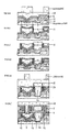
- Fig. 3a
- Lamellenstruktur der Speicherelektrode in der Draufsicht des Speicherzellenlayouts
- Fig. 3b
- STC-Komplex vor RIE der dicken Hilfsisolationsschicht
- Fig. 3c
- STC-Komplex vor RIE der ersten dünnen Hilfsisolationsschicht
- Fig. 3d
- STC-Komplex nach RIE der ersten dünnen Hilfsisolationsschicht
- Fig. 3e
- STC-Komplex nach Abscheidung der letzten auffüllenden Lamellenschicht
- Fig. 3f
- STC-Komplex nach RIE des planaren Lamellenschichtstapels
- Fig. 3g
- STC-Komplex nach isotroper Entfernung der Hilfsisolationsschichten
- Fig. 3h
- STC-Komplex nach maskenfreier RIE-Strukturierung der Bodenplatte
- Fig. 3i
- STC-Komplex Endzustand
- Fig. 4a
- Speicherzellenanordnung "STC on Bitline" vor RIE des Drainkontaktfensters
- Fig. 4b
- Speicherzellenanordnung "STC on Bitline" vor RIE-Strukturierung des leitenden Rings
- Fig. 4c
- Speicherzellenanordnung "STC on Bitline" nach RIE-Strukturierung einer dünnen Isolationsschicht an der Innenfläche des leitenden Rings
- Fig. 4d
- Speicherzellenanordnung "STC on Bitline" nach Abscheidung einer weiteren Isolationsschicht für den Isolationsmantel
- Fig. 4e
- Speicherzellenanordnung "STC on Bitline" vor RIE der dicken Hilfsisolationsschicht
- Fig. 4f
- Speicherzellenanordnung "STC on Bitline" nach Abscheidung der Deckisolationsschicht auf dem kompletten STC-Komplex
- Fig. 1a
- Cell construction scheme of a memory cell arrangement "Bitline on STC" (drawn without a cell plate)
- Fig. 1b
- Cell layout of a memory cell arrangement "Bitline on STC" (drawn without bit line)
- Fig. 1c
- Cross section of a memory cell arrangement "Bitline on STC"
- Fig. 2a
- Cell construction scheme of a memory cell arrangement with "STC on Bitline" (drawn without cell plate: STC complex removed)
- Fig. 2b
- Cell layout of a memory cell arrangement "STC on Bitline" (drawn without bit line)
- Fig. 2c
- Cross section of a memory cell arrangement "STC on Bitline"
- Fig. 3a
- Lamella structure of the storage electrode in the top view of the storage cell layout
- Fig. 3b
- STC complex before RIE of the thick auxiliary insulation layer
- Fig. 3c
- STC complex before RIE of the first thin auxiliary insulation layer
- Fig. 3d
- STC complex according to RIE of the first thin auxiliary insulation layer
- Fig. 3e
- STC complex after deposition of the last filling lamella layer
- 3f
- STC complex according to RIE of the planar lamella layer stack
- Fig. 3g
- STC complex after isotropic removal of the auxiliary insulation layers
- Fig. 3h
- STC complex after mask-free RIE structuring of the base plate
- 3i
- STC complex final state
- Fig. 4a
- Memory cell arrangement "STC on Bitline" in front of RIE of the drain contact window
- Fig. 4b
- "STC on Bitline" memory cell arrangement before RIE structuring of the conductive ring
- Fig. 4c
- "STC on Bitline" memory cell arrangement after RIE structuring of a thin insulation layer on the inner surface of the conductive ring
- Fig. 4d
- "STC on Bitline" memory cell arrangement after deposition of a further insulation layer for the insulation jacket
- Fig. 4e
- "STC on Bitline" memory cell arrangement in front of RIE of the thick auxiliary insulation layer
- Fig. 4f
- "STC on Bitline" memory cell arrangement after deposition of the cover insulation layer on the complete STC complex
Die Realisierung der erfindungsgemäßen Ein-Transistor-Speicherzellenanordnung für dynamische Halbleiterspeicher ist zum einen, wie in Fig. 1 dargestellt, wobei Fig. 1a die Zellenkonstruktion, Fig. 1b das Zellenlayout und Fig. 1c den Querschnitt zeigt, als eine Speicherzellenanordnung mit STC on Bitline und zum anderen, wie in Fig. 2a dargestellt, wobei Fig. 2a die Zellenkonstruktion, Fig. 2b das Zellenlayout und Fig. 2c den Querschnitt zeigt, als eine Speicherzellenanordnung mit Bitline on STC möglich.The realization of the one-transistor memory cell arrangement according to the invention for dynamic semiconductor memories is, on the one hand, as shown in FIG. 1, with FIG. 1a the cell construction, FIG. 1b the cell layout and FIG. 1c the cross section, as a memory cell arrangement with STC on bitline and on the other hand, as shown in FIG. 2a, where FIG. 2a shows the cell construction, FIG. 2b the cell layout and FIG. 2c the cross section, possible as a memory cell arrangement with Bitline on STC.
Die Erfindung soll nachstehend anhand der Herstellung einer STC on Bitline-Speicherzellenanordnung näher erläutert werden.The invention will be explained in more detail below on the basis of the production of an STC on bitline memory cell arrangement.
Nach der Herstellung von n- und p-leitenden CMOS-Wannen werden in einem p-dotiertem Siliziumsubstrat mit einem LOGOS-Verfahren Feldisolationsgebiete und aktive Bereiche und im Anschluß daran LDD-MOS-Transistoren, bestehend aus isolierten Polysilizium-Wortleitungen 12 mit Siliziumdioxiddeckisolation, seitlichen Isolationsspacern und Source- 7 und Draingebieten 9 ausgebildet.After the manufacture of n- and p-type CMOS wells are formed in a p-doped silicon substrate with a LOGOS process field isolation areas and active areas and then LDD-MOS transistors, consisting of isolated polysilicon word lines 12 with silicon dioxide cover insulation, lateral insulation spacers and
Anschließend wird eine 400 nm dicke, verrundete untere Isolationsschicht 11 aufgebracht und strukturiert, wodurch in der Speichermatrix Sourcekontaktfenster 8 geöffnet werden. Nachfolgend wird durch Abscheidung, Dotierung und Strukturierung einer Polycid-Schicht die Bitleitung erzeugt und angeschlossen. Danach wird eine 650 nm dicke, mittels RTA verrundete, obere Isolationsschicht 13 aufgebracht (Fig. 4a) und mit einem RIE-Prozeß über eine Lackmaske in den Draingebieten 9 der n-LDD-MOS-Transistoren der Spelchermatrix steilflankig Drainkontaktfenster 10 mit einer minimalen Kontaktfensterbreite von 1,0 um in die obere Isolationsschicht 13 eingebracht, wobei der Ätzprozeß durch seine Selektivität gegenüber dem Bitleitungsmaterial auf der Bitleitungsoberfläche gestoppt wird.A 400 nm thick, rounded
Mit einem weiteren RIE-Prozeß wird die im Drainkontaktfenster 10 freigelegte Bitleitung 6 durchtrennt, wobei die untere Isolationsschicht 11 bis auf eine verbleibende Restdicke von 200 nm angeätzt wird.Another RIE process cuts through the
Nach der Entfernung der Lackmaske und der Durchführung eines Reinigungsverfahrens wird eine 20 nm dicke, phosphordotierte Polysiliziumschicht abgeschieden. Danach wird eine die Steilflanken des Drainkontaktfensters 10 konform bedeckende 200 nm dicke Wolfram-CVD-Schicht aufgebracht (Fig. 4b) und durch einen folgenden anisotropen RIE-Prozeß von allen horizontalen Flächen wieder entfernt. An den Steilflanken des Drainkontaktfensters 10 bleibt die aus Wolfram und Polysilizium bestehende Doppelschicht jedoch in Form eines leitenden Ringes 16 bestehen. Der leitende Ring 16 kontaktiert die durch den Drainkontaktfensterätzprozeß durchbrochene Bitleitung 6 und schließt sie bis auf das im Zentrum des leitenden Ringes verbleibende Drainkontaktfenster 10 wieder.After removing the resist mask and carrying out a cleaning process, a 20 nm thick, phosphorus-doped polysilicon layer is deposited. Then a 200 nm thick tungsten CVD layer conformally covering the steep flanks of the
Bei diesem RIE-Ätzprozeß erfolgt ein großflächiger Abtrag der oberen Isolationsschicht 13 und im Bereich des verbleibenden Drainkontaktfenster 10 zugleich der unteren Isolationsschicht 11 von ca. 50 nm.In this RIE etching process, the
Im Anschluß an diesen Ätzprozeß wird eine dünne Isolationsschicht 20 in Form einer 50 nm dicken Siliziumnitridschicht mittels eines LPCVD-Verfahrens abgeschieden und durch einen anisotropen RIE-Ätzprozeß von den horizontalen Flächen wieder entfernt, dabei bleibt die Siliziumnitridschicht 20 an der inneren horizontalen Wandfläche des leitenden Ringes 16 mit ungeschwächter Dicke erhalten (Fig. 4c).Following this etching process, a
Anschließend wird die freiliegende obere Deckfläche des leitenden Ringes 16 isotrop und selektiv bis auf ein Niveau von ca. 200 nm oberhalb der Bitleitungsoberfläche abgeätzt, wobei die Siliziumnitridschicht 20 an der inneren vertikalen Wandfläche des leitenden Ringes 16 vollständig erhalten bleibt.The exposed upper cover surface of the
Danach wird eine 140 nm dicke Siliziumschicht mit einem LPCVD-Verfahren abgeschieden (Fig. 4d) und anschließend durch einen anisotropen RIE-Prozeß auf allen horizontalen Flächen wieder entfernt. Durch Fortsetzung des RIE-Prozesses wird nachfolgend das im Zentrum des leitenden Ringes 16 verbleibende Drainkontaktfenster 10 bis auf die Substratoberfläche geöffnet. Der leitende Ring 16 ist somit an seiner oberen Deckfläche und seiner inneren vertikalen Wandfläche durch einen Isolationsmantel 15, der aus beiden maskenfrei strukturierten Siliziumnitridschichten gebildet wird, bedeckt.A 140 nm thick silicon layer is then deposited using an LPCVD process (FIG. 4d) and then removed again on all horizontal surfaces by an anisotropic RIE process. By continuing the RIE process, the
Nach einer Reinigung der verbleibenden freigelegten Drainkontaktfensterfläche 10 wird eine 100 nm dicke n-leitende Polysiliziumschicht als unterste Bodenplattenschicht 2a, die das Draingebiet 9 kontaktiert und das im Zentrum des leitenden Ringes 16 und seines Isolationsmantels 15 verbliebene Drainkontaktfenster 10 in Form eines leitenden Stempels 14 vollständig ausgefüllt, abgeschieden.After the remaining exposed drain
Im Anschluß daran wird eine 1 um dicke planarisierte Hilfsisolatorschicht 17 aufgebracht (Fig. 4e; Fig. 3b) und über eine Lackmaske mit einem anisotropen selektiven RIE-Prozeß, der auf der untersten Bodenplattenschicht 2A gestoppt wird, ein steilflankiger Durchbruch mit einer Breite von 1,6 um in die Hilfsisolatorschicht 17 eingebracht. Nach Entfernung der Lackmaske und der Durchführung eines Reinigungsprozesses wird eine n-leitende Polysiliziumschicht mit einer Dicke von 175 nm als erste leitende Lamellenschicht abgeschieden, danach eine erste dünne Hilfsisolationsschicht 18 mit einer Dicke von 180 nm aufgebracht (Fig. 3c) und anschließend durch einen anisotropen RIE-Prozeß auf allen horizontalen Flächen wieder entfernt, wobei der anisotrope Ätzprozeß auf der ersten Lamellenschicht gestoppt wird (Fig. 3d). Nach einem Reinigungsprozeß wird wiederum eine n-leitende Polysiliziumschicht abgeschieden, eine weitere dünne Hilfsisolationsschicht 18 mit einer Dicke von 180 nm aufgebracht und mit einem anisotropen RIE-Prozeß wieder entfernt, so daß die steilflankigen, vertikalen Seitenwände des Durchbruchs von einer Schicht folge aus Polysiliziumschicht und dünner Hilfsisolatorschicht 18 zweifach bedeckt sind und im Zentrum des Durchbruchs eine Restöffnung von 180 nm minimaler Breite verbleibt. Diese Restöffnung wird durch Abscheidung einer 120 nm dicken n-leitenden Polysiliziumschicht als letzte Lamellenschicht vollständig ausgefüllt (Fig. 3e).Subsequently, a 1 µm thick planarized
Im Anschluß daran wird der auf der Oberfläche der dicken Hilfsisolationsschicht 17 liegende Schichtstapel aller Lamellenschichten mit einem RIE-Prozeß entfernt, wobei die Oberflächen der dicken Hilfsisolationsschicht 17 und der im steilflankigen Durchbruch verbliebenen dünnen Hilfsisolationsschichten 18 freigelegt werden und die oberen Enden der senkrecht im Durchbruch angeordneten Polysiliziumlamellen 3 voneinander getrennt werden (Fig. 3f).The layer stack of all lamella layers lying on the surface of the thick
Nach dem anschließenden selektiven naßchemischen Entfernen der dünnen 18 und der dicken Hilfsisolationsschichten 17 (Fig. 3g) werden die im Bereich des vorherigen steilflankigen Durchbruchs vertikal freistehenden Polysiliziumlamellen 3 durch ein anisotropes RIE-Verfahren vertikal um die Dicke der untersten Bodenplattenschicht 2A abgetragen, wobei das RIE-Verfahren auf der oberen Isolationsschicht 13 gestoppt wird. Durch dieses RIE-Verfahren erfolgt die vollständige selbstjustierende Ätzung der untersten Bodenplattenschicht 2A im Bereich außerhalb des vorherigen steilflankigen Durchbruchs und somit die Trennung der Speicherelektroden 1 benachbarter Speicherzellen, wobei die die leitenden Lamellen horizontal verbindende leitende Bodenplatte 2, die aus der untersten Bodenplattenschicht 2A und den horizontalen Teilen der Polysiliziumlamellenschichten besteht, um die Dicke der untersten Bodenplattenschicht abgedünnt, aber nicht durchtrennt wird (Fig. 3h).After the subsequent selective wet chemical removal of the thin 18 and the thick auxiliary insulation layers 17 (FIG. 3g), the
Im Anschluß an diesen Ätzprozeß wird aus einer 3 nm dicken Polysiliziumschicht, einer 10 nm dicken LPCVD-Siliziumnitridschicht und einer Reoxidation der Siliziumnitridschicht ein ONO-Speicherdielektrikum 4 mit einer Siliziumdioxid-Äquivalentdicke von 3 nm erzeugt.Following this etching process, an
Hiernach wird eine n-dotierte Polysiliziumschicht als Zellplatte 5 mit einer Dicke von 150 nm abgeschieden und strukturiert, die die Räume zwischen den Polysiliziumlamellen 3 vollständig ausfüllt.An n-doped polysilicon layer is then deposited and structured as a
Abschließend wird eine planarisierende Deckisolationsschicht 19 abgeschieden und strukturiert (Fig. 31; Fig. 4f).
- 1 -
- Speicherelektrode
- 2 -
- leitende Bodenplatte der Speicherelektrode
- 2A -
- unterste leitende Bodenplattenschicht
- 3 -
- leitende Lamellen
- 3A -
- äußerste Lamelle
- 3B -
- innerste Lamelle
- 4 -
- Speicherdielektrikum
- 5 -
- Zellplatte
- 6 -
- Bitleitung
- 7 -
- Sourcegebiet
- 8 -
- Source- bzw. Bitleitungskontaktfenster
- 9 -
- Draingebiet
- 10 -
- Drainkontaktfenster
- 11 -
- untere Isolationsschicht
- 12 -
- isolierte Wortleitung
- 13 -
- obere Isolationsschicht
- 14 -
- leitender Stempel für die Drainkontaktierung
- 15 -
- Isolationsmantel
- 16 -
- leitender Ring
- 17 -
- dicke Hilfsisolationsschicht
- 18 -
- dünne Hilfsisolationsschicht
- 19 -
- planarisierende Deckisolationsschicht
- 20 -
- dünne Isolationsschicht
- 21 -
- planarisierter leitfähiger Stempel für die Sourcekontaktierung
- 1 -
- Storage electrode
- 2 -
- conductive bottom plate of the storage electrode
- 2A -
- lowest conductive floor slab layer
- 3 -
- conductive slats
- 3A -
- outermost slat
- 3B -
- innermost slat
- 4 -
- Storage dielectric
- 5 -
- Cell plate
- 6 -
- Bit line
- 7 -
- Source area
- 8th -
- Source or bit line contact window
- 9 -
- Drainage area
- 10 -
- Drain contact window
- 11 -
- lower insulation layer
- 12 -
- isolated word line
- 13 -
- upper insulation layer
- 14 -
- conductive stamp for drain contact
- 15 -
- Insulation jacket
- 16 -
- conductive ring
- 17 -
- thick auxiliary insulation layer
- 18 -
- thin auxiliary insulation layer
- 19 -
- planarizing cover insulation layer
- 20 -
- thin insulation layer
- 21 -
- planarized conductive stamp for source contacting
Claims (10)
Priority Applications (1)
| Application Number | Priority Date | Filing Date | Title |
|---|---|---|---|
| EP94101691A EP0600850B1 (en) | 1990-02-23 | 1991-02-14 | DRAM cell structure with capacitor over bit line and method of making the same |
Applications Claiming Priority (2)
| Application Number | Priority Date | Filing Date | Title |
|---|---|---|---|
| DD338097 | 1990-02-23 | ||
| DD338097A DD299990A5 (en) | 1990-02-23 | 1990-02-23 | One-transistor memory cell arrangement and method for its production |
Related Child Applications (2)
| Application Number | Title | Priority Date | Filing Date |
|---|---|---|---|
| EP94101691A Division EP0600850B1 (en) | 1990-02-23 | 1991-02-14 | DRAM cell structure with capacitor over bit line and method of making the same |
| EP94101691.7 Division-Into | 1991-02-14 |
Publications (3)
| Publication Number | Publication Date |
|---|---|
| EP0443439A2 true EP0443439A2 (en) | 1991-08-28 |
| EP0443439A3 EP0443439A3 (en) | 1991-10-02 |
| EP0443439B1 EP0443439B1 (en) | 1995-10-18 |
Family
ID=5616632
Family Applications (2)
| Application Number | Title | Priority Date | Filing Date |
|---|---|---|---|
| EP94101691A Expired - Lifetime EP0600850B1 (en) | 1990-02-23 | 1991-02-14 | DRAM cell structure with capacitor over bit line and method of making the same |
| EP91102082A Expired - Lifetime EP0443439B1 (en) | 1990-02-23 | 1991-02-14 | One-transistor-storage cell device and method for making the same |
Family Applications Before (1)
| Application Number | Title | Priority Date | Filing Date |
|---|---|---|---|
| EP94101691A Expired - Lifetime EP0600850B1 (en) | 1990-02-23 | 1991-02-14 | DRAM cell structure with capacitor over bit line and method of making the same |
Country Status (4)
| Country | Link |
|---|---|
| EP (2) | EP0600850B1 (en) |
| AT (1) | ATE129363T1 (en) |
| DD (1) | DD299990A5 (en) |
| DE (3) | DE59106693D1 (en) |
Cited By (9)
| Publication number | Priority date | Publication date | Assignee | Title |
|---|---|---|---|---|
| GB2259187A (en) * | 1991-08-31 | 1993-03-03 | Samsung Electronics Co Ltd | Capacitors for semiconductor memory cells |
| GB2259406A (en) * | 1991-09-07 | 1993-03-10 | Samsung Electronics Co Ltd | Semiconductor memory device capacitors |
| US5274258A (en) * | 1991-01-30 | 1993-12-28 | Samsung Electronics Co., Ltd. | High density semiconductor memory device (MBC cell) |
| WO1994000877A1 (en) * | 1992-06-30 | 1994-01-06 | Siemens Aktiengesellschaft | Process for producing a storage capacitor |
| WO1994001891A1 (en) * | 1992-07-08 | 1994-01-20 | Siemens Aktiengesellschaft | Process for producing storage capacitors for dram cells |
| EP0595360A1 (en) * | 1992-10-30 | 1994-05-04 | Nec Corporation | Method of manufacturing a semiconductor device having a cylindrical electrode |
| GB2279176A (en) * | 1991-05-23 | 1994-12-21 | Samsung Electronics Co Ltd | Dram cell capacitor |
| GB2297648A (en) * | 1991-08-31 | 1996-08-07 | Samsung Electronics Co Ltd | Capacitors for semiconductor memory cells |
| FR2761198A1 (en) * | 1997-03-07 | 1998-09-25 | United Microelectronics Corp | POLYSILICON CMP PROCESS FOR HIGH DENSITY DRAM CELL STRUCTURES |
Families Citing this family (4)
| Publication number | Priority date | Publication date | Assignee | Title |
|---|---|---|---|---|
| KR940006587B1 (en) * | 1991-05-23 | 1994-07-22 | 삼성전자 주식회사 | Manufacturing method of capacitor of DRAM cell |
| US5150276A (en) * | 1992-01-24 | 1992-09-22 | Micron Technology, Inc. | Method of fabricating a vertical parallel cell capacitor having a storage node capacitor plate comprising a center fin effecting electrical communication between itself and parallel annular rings |
| KR950021644A (en) * | 1993-12-31 | 1995-07-26 | 김주용 | Semiconductor Memory and Manufacturing Method |
| KR0126640B1 (en) * | 1994-05-07 | 1998-04-02 | 김주용 | Semiconductor device and manufacturing method |
Family Cites Families (9)
| Publication number | Priority date | Publication date | Assignee | Title |
|---|---|---|---|---|
| US4855801A (en) * | 1986-08-22 | 1989-08-08 | Siemens Aktiengesellschaft | Transistor varactor for dynamics semiconductor storage means |
| JP2702121B2 (en) * | 1987-02-25 | 1998-01-21 | 日本電気株式会社 | Semiconductor storage device |
| US4872050A (en) * | 1988-03-15 | 1989-10-03 | Mitsubishi Denki Kabushiki Kaisha | Interconnection structure in semiconductor device and manufacturing method of the same |
| JP2755591B2 (en) * | 1988-03-25 | 1998-05-20 | 株式会社東芝 | Semiconductor storage device |
| JPH01302852A (en) * | 1988-05-31 | 1989-12-06 | Fujitsu Ltd | Structure of memory cell of semiconductor memory |
| JPH01302851A (en) * | 1988-05-31 | 1989-12-06 | Fujitsu Ltd | Structure of memory cell of semiconductor memory |
| JPH01308069A (en) * | 1988-06-07 | 1989-12-12 | Fujitsu Ltd | Memory cell structure of semiconductor memory |
| DE3918924C2 (en) * | 1988-06-10 | 1996-03-21 | Mitsubishi Electric Corp | Manufacturing method for a semiconductor memory device |
| JP2724209B2 (en) * | 1989-06-20 | 1998-03-09 | シャープ株式会社 | Method for manufacturing semiconductor memory device |
-
1990
- 1990-02-23 DD DD338097A patent/DD299990A5/en unknown
-
1991
- 1991-02-14 EP EP94101691A patent/EP0600850B1/en not_active Expired - Lifetime
- 1991-02-14 AT AT91102082T patent/ATE129363T1/en not_active IP Right Cessation
- 1991-02-14 DE DE59106693T patent/DE59106693D1/en not_active Expired - Fee Related
- 1991-02-14 DE DE59109236T patent/DE59109236D1/en not_active Expired - Fee Related
- 1991-02-14 EP EP91102082A patent/EP0443439B1/en not_active Expired - Lifetime
- 1991-02-19 DE DE4105501A patent/DE4105501A1/en not_active Withdrawn
Cited By (15)
| Publication number | Priority date | Publication date | Assignee | Title |
|---|---|---|---|---|
| US5274258A (en) * | 1991-01-30 | 1993-12-28 | Samsung Electronics Co., Ltd. | High density semiconductor memory device (MBC cell) |
| GB2279176B (en) * | 1991-05-23 | 1995-06-07 | Samsung Electronics Co Ltd | DRAM cell capacitor |
| GB2279176A (en) * | 1991-05-23 | 1994-12-21 | Samsung Electronics Co Ltd | Dram cell capacitor |
| GB2259187B (en) * | 1991-08-31 | 1996-06-19 | Samsung Electronics Co Ltd | Semiconductor device |
| US5330614A (en) * | 1991-08-31 | 1994-07-19 | Samsung Electronics Co., Ltd. | Manufacturing method of a capacitor having a storage electrode whose sidewall is positively inclined with respect to the horizontal surface |
| FR2680913A1 (en) * | 1991-08-31 | 1993-03-05 | Samsung Electronics Co Ltd | SEMICONDUCTOR MEMORY DEVICE HAVING CAPACITOR AND METHOD FOR MANUFACTURING SAME. |
| GB2259187A (en) * | 1991-08-31 | 1993-03-03 | Samsung Electronics Co Ltd | Capacitors for semiconductor memory cells |
| GB2297648A (en) * | 1991-08-31 | 1996-08-07 | Samsung Electronics Co Ltd | Capacitors for semiconductor memory cells |
| GB2297648B (en) * | 1991-08-31 | 1996-10-23 | Samsung Electronics Co Ltd | Semiconductor device |
| GB2259406B (en) * | 1991-09-07 | 1996-05-01 | Samsung Electronics Co Ltd | Semiconductor memory devices |
| GB2259406A (en) * | 1991-09-07 | 1993-03-10 | Samsung Electronics Co Ltd | Semiconductor memory device capacitors |
| WO1994000877A1 (en) * | 1992-06-30 | 1994-01-06 | Siemens Aktiengesellschaft | Process for producing a storage capacitor |
| WO1994001891A1 (en) * | 1992-07-08 | 1994-01-20 | Siemens Aktiengesellschaft | Process for producing storage capacitors for dram cells |
| EP0595360A1 (en) * | 1992-10-30 | 1994-05-04 | Nec Corporation | Method of manufacturing a semiconductor device having a cylindrical electrode |
| FR2761198A1 (en) * | 1997-03-07 | 1998-09-25 | United Microelectronics Corp | POLYSILICON CMP PROCESS FOR HIGH DENSITY DRAM CELL STRUCTURES |
Also Published As
| Publication number | Publication date |
|---|---|
| EP0600850A1 (en) | 1994-06-08 |
| EP0600850B1 (en) | 2002-05-29 |
| DE59109236D1 (en) | 2002-07-04 |
| DE4105501A1 (en) | 1991-08-29 |
| DD299990A5 (en) | 1992-05-14 |
| EP0443439B1 (en) | 1995-10-18 |
| EP0443439A3 (en) | 1991-10-02 |
| ATE129363T1 (en) | 1995-11-15 |
| DE59106693D1 (en) | 1995-11-23 |
Similar Documents
| Publication | Publication Date | Title |
|---|---|---|
| DE102004003315B4 (en) | Semiconductor device with electrical contact and method of making the same | |
| DE3788499T2 (en) | Semiconductor trench capacitor structure. | |
| DE4016686C2 (en) | Method of manufacturing a semiconductor memory | |
| DE3525418A1 (en) | SEMICONDUCTOR STORAGE DEVICE AND METHOD FOR THEIR PRODUCTION | |
| DE3785317T2 (en) | High packing density matrix made of dynamic VMOS RAM. | |
| DE4028488A1 (en) | SEMICONDUCTOR STORAGE DEVICE AND METHOD FOR THEIR PRODUCTION | |
| DE4126046A1 (en) | MANUFACTURING METHOD AND STRUCTURE OF A DRAM MEMORY CELL CAPACITOR | |
| EP0936673B1 (en) | Memory cell array and corresponding manufacturing process | |
| DE10128718B4 (en) | Trench capacitor of a DRAM memory cell with metallic collarbear and non-metallic conduction bridge to the select transistor | |
| EP0875937A2 (en) | DRAM cell array and method of making the same | |
| EP0443439A2 (en) | One-transistor-storage cell device and method for making the same | |
| DE4029256A1 (en) | STACK CAPACITOR OF A DRAM STORAGE CELL AND METHOD FOR PRODUCING THE SAME | |
| EP0987753A2 (en) | Stacked DRAM fin capacitor and method of making the same | |
| EP1125328B1 (en) | Method for producing a dram cell arrangement | |
| DE19706533A1 (en) | Semiconductor component with electric separation of adjacent element forming regions | |
| EP0945901A1 (en) | DRAM cell array with vertical transistors and process of manufacture | |
| DE19832095C1 (en) | Stacked capacitor manufacturing process | |
| DE19929211B4 (en) | A method of manufacturing a MOS transistor and a DRAM cell array | |
| DE4203565A1 (en) | DRAM AND METHOD FOR THE PRODUCTION THEREOF | |
| DE10334547B4 (en) | A manufacturing method for a trench capacitor with an insulation collar, which is electrically connected on one side to a substrate via a buried contact | |
| DE10239488A1 (en) | Production of a trench dynamic random access memory cell in a semiconductor substrate involves forming pad nitride on substrate and ion etching trench vertically to first depth, depositing nitride layer in the trench and further treating | |
| EP0399060B1 (en) | Semiconductor memory arrangement using capacitors with two electrodes situated inside a groove, and method of producing the same | |
| WO2000060666A1 (en) | Memory cell unit and method of producing same | |
| DD280851A1 (en) | METHOD OF MAKING TRENCH MEMORY CELLS | |
| DE10333777B4 (en) | A manufacturing method for a trench capacitor with an insulation collar, which is electrically connected on one side to a substrate via a buried contact, in particular for a semiconductor memory cell |
Legal Events
| Date | Code | Title | Description |
|---|---|---|---|
| PUAI | Public reference made under article 153(3) epc to a published international application that has entered the european phase |
Free format text: ORIGINAL CODE: 0009012 |
|
| PUAL | Search report despatched |
Free format text: ORIGINAL CODE: 0009013 |
|
| AK | Designated contracting states |
Kind code of ref document: A2 Designated state(s): AT CH DE FR GB IT LI NL |
|
| AK | Designated contracting states |
Kind code of ref document: A3 Designated state(s): AT CH DE FR GB IT LI NL |
|
| 17P | Request for examination filed |
Effective date: 19911017 |
|
| RAP1 | Party data changed (applicant data changed or rights of an application transferred) |
Owner name: INSTITUT FUER HALBLEITERPHYSIK FRANKFURT (ODER) GM |
|
| 17Q | First examination report despatched |
Effective date: 19930827 |
|
| GRAA | (expected) grant |
Free format text: ORIGINAL CODE: 0009210 |
|
| AK | Designated contracting states |
Kind code of ref document: B1 Designated state(s): AT CH DE FR GB IT LI NL |
|
| PG25 | Lapsed in a contracting state [announced via postgrant information from national office to epo] |
Ref country code: IT Free format text: LAPSE BECAUSE OF FAILURE TO SUBMIT A TRANSLATION OF THE DESCRIPTION OR TO PAY THE FEE WITHIN THE PRE;WARNING: LAPSES OF ITALIAN PATENTS WITH EFFECTIVE DATE BEFORE 2007 MAY HAVE OCCURRED AT ANY TIME BEFORE 2007. THE CORRECT EFFECTIVE DATE MAY BE DIFFERENT FROM THE ONE RECORDED.SCRIBED TIME-LIMIT Effective date: 19951018 Ref country code: NL Free format text: LAPSE BECAUSE OF FAILURE TO SUBMIT A TRANSLATION OF THE DESCRIPTION OR TO PAY THE FEE WITHIN THE PRESCRIBED TIME-LIMIT Effective date: 19951018 |
|
| REF | Corresponds to: |
Ref document number: 129363 Country of ref document: AT Date of ref document: 19951115 Kind code of ref document: T |
|
| XX | Miscellaneous (additional remarks) |
Free format text: TEILANMELDUNG 94101691.7 EINGEREICHT AM 14/02/91. |
|
| REF | Corresponds to: |
Ref document number: 59106693 Country of ref document: DE Date of ref document: 19951123 |
|
| PG25 | Lapsed in a contracting state [announced via postgrant information from national office to epo] |
Ref country code: GB Effective date: 19960214 |
|
| REG | Reference to a national code |
Ref country code: CH Ref legal event code: NV Representative=s name: A. BRAUN, BRAUN, HERITIER, ESCHMANN AG PATENTANWAE |
|
| ET | Fr: translation filed | ||
| NLV1 | Nl: lapsed or annulled due to failure to fulfill the requirements of art. 29p and 29m of the patents act | ||
| GBV | Gb: ep patent (uk) treated as always having been void in accordance with gb section 77(7)/1977 [no translation filed] |
Effective date: 19951213 |
|
| GBT | Gb: translation of ep patent filed (gb section 77(6)(a)/1977) |
Effective date: 19960524 |
|
| PLBE | No opposition filed within time limit |
Free format text: ORIGINAL CODE: 0009261 |
|
| STAA | Information on the status of an ep patent application or granted ep patent |
Free format text: STATUS: NO OPPOSITION FILED WITHIN TIME LIMIT |
|
| GBPC | Gb: european patent ceased through non-payment of renewal fee |
Effective date: 19960214 |
|
| 26N | No opposition filed | ||
| REG | Reference to a national code |
Ref country code: CH Ref legal event code: PUE Owner name: INSTITUT FUER HALBLEITERPHYSIK FRANKFURT (ODER) GM Ref country code: CH Ref legal event code: NV Representative=s name: SIEMENS SCHWEIZ AG |
|
| REG | Reference to a national code |
Ref country code: FR Ref legal event code: TP |
|
| PGFP | Annual fee paid to national office [announced via postgrant information from national office to epo] |
Ref country code: CH Payment date: 20010511 Year of fee payment: 11 |
|
| PGFP | Annual fee paid to national office [announced via postgrant information from national office to epo] |
Ref country code: AT Payment date: 20020123 Year of fee payment: 12 |
|
| PG25 | Lapsed in a contracting state [announced via postgrant information from national office to epo] |
Ref country code: CH Free format text: LAPSE BECAUSE OF NON-PAYMENT OF DUE FEES Effective date: 20020228 Ref country code: LI Free format text: LAPSE BECAUSE OF NON-PAYMENT OF DUE FEES Effective date: 20020228 |
|
| REG | Reference to a national code |
Ref country code: CH Ref legal event code: PL |
|
| PG25 | Lapsed in a contracting state [announced via postgrant information from national office to epo] |
Ref country code: AT Free format text: LAPSE BECAUSE OF NON-PAYMENT OF DUE FEES Effective date: 20030214 |
|
| PGFP | Annual fee paid to national office [announced via postgrant information from national office to epo] |
Ref country code: DE Payment date: 20050421 Year of fee payment: 15 |
|
| PGFP | Annual fee paid to national office [announced via postgrant information from national office to epo] |
Ref country code: FR Payment date: 20060216 Year of fee payment: 16 |
|
| PG25 | Lapsed in a contracting state [announced via postgrant information from national office to epo] |
Ref country code: DE Free format text: LAPSE BECAUSE OF NON-PAYMENT OF DUE FEES Effective date: 20060901 |
|
| REG | Reference to a national code |
Ref country code: FR Ref legal event code: ST Effective date: 20071030 |
|
| PG25 | Lapsed in a contracting state [announced via postgrant information from national office to epo] |
Ref country code: FR Free format text: LAPSE BECAUSE OF NON-PAYMENT OF DUE FEES Effective date: 20070228 |