EP0443603A2 - Semiconductor device - Google Patents
Semiconductor device Download PDFInfo
- Publication number
- EP0443603A2 EP0443603A2 EP91102621A EP91102621A EP0443603A2 EP 0443603 A2 EP0443603 A2 EP 0443603A2 EP 91102621 A EP91102621 A EP 91102621A EP 91102621 A EP91102621 A EP 91102621A EP 0443603 A2 EP0443603 A2 EP 0443603A2
- Authority
- EP
- European Patent Office
- Prior art keywords
- film thickness
- insulating film
- film
- transistor
- gate insulating
- Prior art date
- Legal status (The legal status is an assumption and is not a legal conclusion. Google has not performed a legal analysis and makes no representation as to the accuracy of the status listed.)
- Withdrawn
Links
- 239000004065 semiconductor Substances 0.000 title claims abstract description 21
- 239000000758 substrate Substances 0.000 description 24
- 239000011229 interlayer Substances 0.000 description 11
- 238000000034 method Methods 0.000 description 11
- 230000000694 effects Effects 0.000 description 10
- 230000005684 electric field Effects 0.000 description 5
- 239000010410 layer Substances 0.000 description 5
- 238000009792 diffusion process Methods 0.000 description 4
- 238000004518 low pressure chemical vapour deposition Methods 0.000 description 4
- 230000008878 coupling Effects 0.000 description 3
- 238000010168 coupling process Methods 0.000 description 3
- 238000005859 coupling reaction Methods 0.000 description 3
- 239000000203 mixture Substances 0.000 description 3
- 238000007254 oxidation reaction Methods 0.000 description 3
- 230000002093 peripheral effect Effects 0.000 description 3
- 238000009413 insulation Methods 0.000 description 2
- 150000004767 nitrides Chemical class 0.000 description 2
- 238000007669 thermal treatment Methods 0.000 description 2
- 239000008186 active pharmaceutical agent Substances 0.000 description 1
- 239000004411 aluminium Substances 0.000 description 1
- 229910052782 aluminium Inorganic materials 0.000 description 1
- XAGFODPZIPBFFR-UHFFFAOYSA-N aluminium Chemical compound [Al] XAGFODPZIPBFFR-UHFFFAOYSA-N 0.000 description 1
- 238000005229 chemical vapour deposition Methods 0.000 description 1
- 230000003247 decreasing effect Effects 0.000 description 1
- 230000002950 deficient Effects 0.000 description 1
- 239000012535 impurity Substances 0.000 description 1
- 238000004519 manufacturing process Methods 0.000 description 1
- 229910052751 metal Inorganic materials 0.000 description 1
- 239000002184 metal Substances 0.000 description 1
- 230000001590 oxidative effect Effects 0.000 description 1
- 238000000206 photolithography Methods 0.000 description 1
- 229910021420 polycrystalline silicon Inorganic materials 0.000 description 1
- 229920005591 polysilicon Polymers 0.000 description 1
- 229920006395 saturated elastomer Polymers 0.000 description 1
- 229910052710 silicon Inorganic materials 0.000 description 1
- 239000010703 silicon Substances 0.000 description 1
- 239000002356 single layer Substances 0.000 description 1
Images


Classifications
-
- H—ELECTRICITY
- H10—SEMICONDUCTOR DEVICES; ELECTRIC SOLID-STATE DEVICES NOT OTHERWISE PROVIDED FOR
- H10B—ELECTRONIC MEMORY DEVICES
- H10B41/00—Electrically erasable-and-programmable ROM [EEPROM] devices comprising floating gates
- H10B41/40—Electrically erasable-and-programmable ROM [EEPROM] devices comprising floating gates characterised by the peripheral circuit region
- H10B41/42—Simultaneous manufacture of periphery and memory cells
- H10B41/49—Simultaneous manufacture of periphery and memory cells comprising different types of peripheral transistor
-
- H—ELECTRICITY
- H10—SEMICONDUCTOR DEVICES; ELECTRIC SOLID-STATE DEVICES NOT OTHERWISE PROVIDED FOR
- H10B—ELECTRONIC MEMORY DEVICES
- H10B41/00—Electrically erasable-and-programmable ROM [EEPROM] devices comprising floating gates
-
- H—ELECTRICITY
- H10—SEMICONDUCTOR DEVICES; ELECTRIC SOLID-STATE DEVICES NOT OTHERWISE PROVIDED FOR
- H10D—INORGANIC ELECTRIC SEMICONDUCTOR DEVICES
- H10D64/00—Electrodes of devices having potential barriers
- H10D64/01—Manufacture or treatment
- H10D64/031—Manufacture or treatment of data-storage electrodes
- H10D64/035—Manufacture or treatment of data-storage electrodes comprising conductor-insulator-conductor-insulator-semiconductor structures
Definitions
- the present invention relates to a semiconductor device and, more particularly, it relates to an electrically erasable and programmable non-volatile semiconductor device (EEPROM).
- EEPROM electrically erasable and programmable non-volatile semiconductor device
- the EEPROM electrically erasable and programmable ROM is well known as the electrically erasable and programmable non-volatile memory.
- the EEPROM similar to the EPROM memorizes information responsive to charges stored in the memory cell and uses tunnel phenomenon to transfer charges at its programming and erasing processes wherein electrons are sent to and received by the floating gate, using tunnel current which passes through a thin tunnel insulating film on the substrate.
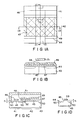
- Fig. 1A is a pattern plan showing an arrangement of one cell of the conventional EEPROM
- Fig. 1B is a sectional view taken along a line IB - IB in Fig. 1A
- Fig. 1C a sectional view taken along a line IC - IC in Fig. 1A
- Fig. 1D a sectional view showing a logic transistor which is a component formed on the same substrate as the memory and cell is to form a large-scale logic circuit such as the gate array.
- the cell which represents 1 bit comprises a selection transistor 41 for preventing half-selection and a memory transistor 42 for storing information.
- a selection gate 46 and a floating gate 47 are formed, adjacent to each other and with a gates insulating film 45 interposed between a semiconductor substrate 43 and them, at an element region separated from each other on the substrate 43 by elements separating regions 44, and a control gate 49 is further formed there with an inter-layer insulating film 48 interposed between the floating gate 47 and it.
- Reference numeral 50 denotes a diffusion layer which has a conductivity type reverse to that of the substrate, and reference numeral 51 an aluminium wiring formed on the interlayer insulating film.
- Information is stored in the electrically floating gate 47 of the memory transistor 42.
- the memory transistor is on- and off-controlled responsive to electrons stored and missed in the floating gate 47. That region of a tunnel insulating film 52 which corresponds to a thinner part (about 100 ⁇ , for example) of the gates insulating film 45 is used to store and miss electrons in the floating gate 47. Namely, tunnel current flows through the tunnel insulating film 52 due to bias added between the control gate 49 and the diffusion layer 50. Electrons are thus sent to and received by the floating gate 47.
- a gate electrode 53 is formed on the same substrate 43 with the gates insulating film 45 interposed between the substrate and the electrode, and the diffusion region which has a conductivity reverse to that of the substrate is formed separating from the gate electrode 53.
- An electric current needed to write and erase information in and from the cell may be small in the case of the EEPROM which uses the tunnel phenomenon.
- Most of the EEPROMs include a boosting circuit (not shown) to create high voltage in the elements and they are made operative by a single power source (about 5V, for example).
- high voltage (about 20V) is added from the boosting circuit to the memory cell and the gate electrode of the selection transistor shown in Figs. 1A through 1C and common power source voltage (about 5V) is added to the gate electrode of the logic transistor shown in Fig. 1D.
- the gates insulating film has the same film thickness (h) (about 450 ⁇ , for example) except the region of the tunnel insulating film 52.
- the gates insulating film used by the conventional EEPROMs is formed to have a film thickness of about 450 ⁇ in all of the transistors of the high voltage and 5V types except the tunnel insulating film whose film thickness is about 100 ⁇ .
- the logic transistor When arranged in this manner, the logic transistor has a film thickness of 450 ⁇ which is the same as that of the high voltage gates insulating film, although its operation voltage is 5V supplied from the common power source. This causes the following problems: Firstly, operation speed becomes low.
- I DS Current I DS between the drain and the source is usually calculated to assume the operation speed of a single transistor. As this I DS becomes larger, the operation speed becomes higher.
- C OX ⁇ O ⁇ I S / d I
- ⁇ represents the mobility in channel
- C OX the capacity of gates insulating film
- W the width of channel
- L the length of channel
- V TH the threshold value
- d I the film thickness of insulating film
- ⁇ O the dielectric constant in vacuum
- ⁇ I the relative dielectric constant of insulating film
- S area of electrode
- I DS is decreased as the film thickness d I of insulating film becomes larger.
- the operation speed of the transistor becomes lower.
- V TH becomes larger and the short channel effect becomes higher as the film thickness of the insulating film becomes larger. This prevents the circuit from being integrated to an extent as greater as possible.
- the gates insulating film of each of transistors is formed to have the same film thickness except the region of the tunnel insulating film without taking voltages used into consideration.
- the present invention is intended to eliminate the above-mentioned drawbacks and the object of the present invention is therefore to provide a semiconductor device enabling logic transistors to be more highly enhanced in their capability and to be more highly integrated, wherein the logic transistors form a circuit located in the periphery of a memory cell and a large-scale logic circuit which are made operative by voltage supplied from the common power source.
- a semiconductor device comprises a first MOS transistor provided with a first gates insulating film which has a first film thickness; a second MOS transistor provided with a second insulating film, said second insulating film including a first portion whose film thickness is the same as the first film thickness and a second portion which has a second film thickness smaller than the first film thickness; and a third MOS transistor provided with a third insulating film which has a third film thickness smaller than the first film thickness.
- the first MOS transistor is made operative by a first gate voltage and the third MOS transistor is made operative by a second gate voltage lower than the first gate voltage.
- the second MOS transistor is of the memory type having an electrically floating gate arranged on the second gates insulating film
- the first MOS transistor is of the selection type for the memory transistor
- the third MOS transistor is of the logic type which is a component for forming the large-scale logic circuit.
- the film thickness of the gates insulating film of the logic transistor which is a component for forming a circuit located in the periphery of the EEPROM or a large-scale logic circuit formed in a mixture on the same semiconductor substrate as the EEPROM is, both of these circuits being made operative by 5V, for example, is made smaller than that of the gates insulating film of each of cells and transistors to which high voltage is added to achieve programming and erasing processes.
- drain current is increased by new transistors formed by the gates insulating films and the operation speed of each of the circuits can be thus enhanced.
- that part of threshold value which is changed by the short channel effect can be suppressed.
- Figs. 2A through 2C are sectional views showing arrangements of transistors forming an example of the EEPROM according to the present invention, in which Fig. 2A is a sectional view showing the transistor arrangement of the high voltage type located at the peripheral region of the memory cell which is made operative by boosted high voltage (20V), Fig. 2B a sectional view showing the arrangement of the memory cell transistor, and Fig. 2C a sectional view showing the arrangement of one channel transistor of CMOS transistors of the logic system for forming memory cell peripheral and large-scale logic circuits which are made operative by common power voltage (5V).
- Fig. 2A is a sectional view showing the transistor arrangement of the high voltage type located at the peripheral region of the memory cell which is made operative by boosted high voltage (20V)
- Fig. 2B a sectional view showing the arrangement of the memory cell transistor
- Fig. 2C a sectional view showing the arrangement of one channel transistor of CMOS transistors of the logic system for forming memory cell peripheral and large-scale logic circuit
- Transistors shown in Figs. 2A through 2C are mounted in a mixture on the same semiconductor substrate 11.
- a diffusion region 12 whose conductivity is reverse to that of the substrate is formed in the substrate.
- a gate insulating film is formed between the substrate and the gate electrode 13-1 and an interlayer insulating film 14 is formed between the gate electrodes 13-1 and a gate electrode 13-2.
- Broken lines 15 in Fig. 2C show gate side wall sections for forming the LDD (lightly doped drain) structure.
- gate insulating films used for the EEPROM include a tunnel insulating film 16 in the memory cell, an insulating film 17 of 5V type in the transistor of the logic type, and an insulating film 18 of the high voltage type in the memory cell and transistor of the high voltage type and each of these insulating films has a film thickness different from those of the others.
- the gate insulating film in the transistor of the logic type shown in Fig. 2C and made operative by common power source voltage (5V) is formed as the insulating film 17 of 5V type whose film thickness is made smaller than that of the insulating film 18 of the high voltage type.
- the insulating film 18 of the high voltage type has a film thickness of about 450A and the insulating film 17 of 5V type has a film thickness of about 250 ⁇ . This enables the 5V transistor of the logic type to be made higher in speed and short channel effect to be suppressed. Further, the capacity of the transistor to be integrated can be increased.
- the tunnel insulating film 16 which needs high electric field for charge transfer is the thinnest.
- the film thickness of the tunnel insulating film 16 is often determined by the capacitive coupling rate which represents the coupling rate of memory transistors.
- the capacitive coupling rate is a parameter for representing whether writing is easy or difficult at the time when charge is received by the floating gate. When this rate is large, it represents that writing is easy.
- the film thickness A (shown in Fig. 2B) of the tunnel insulating film 16 must be about 100 ⁇ from this point of view.
- the insulating film 18 of the high pressure-tight type to which voltage of 20V is added will be now described.
- the insulating film 18 usually has a film thickness of about 450 ⁇ . Electric field added to the insulating film 18 is about 4.4MV/cm. If it is worried whether or not this film thickness of about 450 ⁇ is large enough to the electric field added, it may be made larger to some extent. It is therefore asked that the film thickness C (shown in Fig. 2A) of the high voltage insulating film 18 is larger than 450 ⁇ .
- the 5V insulating film 17 which is used under the power source voltage of 5V will be now described.
- the film thickness B (shown in Fig. 2C) of the insulating film 17 is about 250 ⁇ . It is not limited particularly to this value of 250 ⁇ but as it becomes larger, the operation speed is made lower and change and irregularity in threshold value are made more remarkable because of short channel effect. As it becomes smaller, effects reverse to the above can be expected.
- the lower limit of it is determined by electric field added to the insulating film 17, but it is allowed to be about 120 ⁇ .
- the gate insulating films used for the EEPROM are generally grouped into three including the tunnel insulating film 16, the 5V insulating film 18 and the high voltage insulating film 18 which are different in film thickness from one another.
- the film thickness of the tunnel insulating film is represented by A
- the film thickness of the 5V insulating film by B and the film thickness of the high voltage insulating film by C A ⁇ B ⁇ C ...
- a ⁇ B in the above relation is an essential term because the range of film thicknesses which the tunnel insulating film 16 is allowed to have is quite narrow so as to let the tunnel insulating film 16 have such characteristics as described above and the tunnel insulating film 16 cannot be made as thick as desired and because the lower limit value of the 5V insulating film 17 which is determined by electric field added must be 120 ⁇ (4.2MV/cm), considering the number of defective transistors produced in the course of the manufacturing process and the reliability of transistors produced as complete ones.
- the film thickness A of the tunnel insulating film 16 is 80 ⁇ , for example, it can be calculated from the equation (2) that the film thickness B of the 5V insulating film 17 is 168 ⁇ 41 ⁇ and that the film thickness C of the high voltage insulating film 18 is 336 ⁇ 82 ⁇ .
- the film thickness A is set to be 80 ⁇ , therefore, the boosted voltage which was conventionally needed to be 20V can be reduced to an extent of about 17V. In this case, however, it is needed that the interlayer insulating film 14 is made thicker at the same time.
- each of the insulating films is designed so as to enable each of the transistors thus produced to attain its maximum capability and that the ratio of these film thicknesses is defined, as described above, considering the scaling of these insulating films.
- Figs. 3A through 3C are sectional views showing the process of making each of the transistors shown in Fig. 2A through 2C to provide an example of the semiconductor device according to the present invention.
- a region of the high voltage type which forms the high voltage transistor, a memory cell region which forms the memory cell transistor, and a region of the 5V type which forms the logic transistor are present from left to right in Figs. 3A through 3C, and they are formed in a mixture on the same substrate.
- the interlayer insulating film between the floating and the control gate is a single layer.
- the substrate 21 is thermal-oxidized to form a gates insulating film 23 of the high voltage type which has a desired film thickness (Fig. 3A).
- a tunnel insulating film 24 is formed by thermal oxidization and a first conductive film 25 is then formed by LPCVD (low pressure CVD) method. After thermal treatment, those portions of the first conductive film 25 and the gates insulating film 23 which extend over the 5V region are etching-removed, using the photolithography again, and that top of the substrate 21 which corresponds to an element active portion at the 5V region is exposed (Fig. 3B).
- the gates insulating film 27 has a film thickness only half that of the interlayer insulating film 26 on the first conductive film (polysilicon) because it is developed from the substrate.
- the gates insulating film 27 is formed in this manner to have a desired film thickness and a second conductive film 28 is then formed and thermal-treated (Fig. 3C).
- the first conductive film becomes a floating gate and the second conductive film becomes a control gate at the memory region.
- the high voltage transistor is used after the first and the second conductive film are short-circuited with each other through a metal wiring or the second conductive film is removed.
- Figs. 4A through 4C are sectional views showing the process of making each of the transistors shown in Figs. 2A through 2C to provide another example of the semiconductor device according to the present invention.
- the interlayer insulating film between the floating and the control gate comprises two or more insulating films whose relative dielectric constants are different from one another.
- the interlayer insulating film comprises an oxide film, a nitride film and an oxide film.
- An elements separating insulation film 32 is formed on a semiconductor substrate 31 and the substrate is then thermal-oxidized to form a gates insulating film 33 of the high voltage type which has a desired film thickness (Fig. 4A).
- the memory cell region is bored only at the tunnel window portion thereof, using the photolithographic technique, until the substrate 31 is exposed.
- a tunnel insulating film 34 is formed by thermal oxidization
- a first conductive film 35 is formed by LPCVD (low pressure chemical vapor deposition) method.
- LPCVD low pressure chemical vapor deposition
- an oxide film, a nitride film and an oxide film are successively formed by thermal oxidizing or CVD method to form an interlayer insulating film 36.
- a gates insulating film 37 of the 5V type is then formed by thermal oxidization to have a desired film thickness and a second conductive film 38 is formed and thermal-treated (Fig. 4C).
- drain current can be increased and operation speed can be enhanced in the operation time of the logic transistor which is made operative by the common power source voltage of 5V and which is a component for forming the memory cell peripheral and large-scale logic circuits.
- short channel effect caused when these circuits are smaller-sized can be suppressed and the circuits can be thus integrated to a greater extent.
Landscapes
- Engineering & Computer Science (AREA)
- Manufacturing & Machinery (AREA)
- Non-Volatile Memory (AREA)
- Semiconductor Memories (AREA)
- Metal-Oxide And Bipolar Metal-Oxide Semiconductor Integrated Circuits (AREA)
Abstract
Description
- The present invention relates to a semiconductor device and, more particularly, it relates to an electrically erasable and programmable non-volatile semiconductor device (EEPROM).
- The EEPROM (electrically erasable and programmable ROM is well known as the electrically erasable and programmable non-volatile memory. The EEPROM similar to the EPROM memorizes information responsive to charges stored in the memory cell and uses tunnel phenomenon to transfer charges at its programming and erasing processes wherein electrons are sent to and received by the floating gate, using tunnel current which passes through a thin tunnel insulating film on the substrate.
- Fig. 1A is a pattern plan showing an arrangement of one cell of the conventional EEPROM, Fig. 1B is a sectional view taken along a line IB - IB in Fig. 1A, Fig. 1C a sectional view taken along a line IC - IC in Fig. 1A and Fig. 1D a sectional view showing a logic transistor which is a component formed on the same substrate as the memory and cell is to form a large-scale logic circuit such as the gate array.
- In Figs. 1A through 1D, the cell which represents 1 bit (unit of information) comprises a
selection transistor 41 for preventing half-selection and amemory transistor 42 for storing information. Namely, aselection gate 46 and afloating gate 47 are formed, adjacent to each other and with agates insulating film 45 interposed between asemiconductor substrate 43 and them, at an element region separated from each other on thesubstrate 43 byelements separating regions 44, and acontrol gate 49 is further formed there with an inter-layer insulatingfilm 48 interposed between thefloating gate 47 and it.Reference numeral 50 denotes a diffusion layer which has a conductivity type reverse to that of the substrate, andreference numeral 51 an aluminium wiring formed on the interlayer insulating film. - Information is stored in the electrically floating
gate 47 of thememory transistor 42. The memory transistor is on- and off-controlled responsive to electrons stored and missed in thefloating gate 47. That region of atunnel insulating film 52 which corresponds to a thinner part (about 100Å, for example) of thegates insulating film 45 is used to store and miss electrons in thefloating gate 47. Namely, tunnel current flows through thetunnel insulating film 52 due to bias added between thecontrol gate 49 and thediffusion layer 50. Electrons are thus sent to and received by thefloating gate 47. - In the case of the logic transistor which serves to form the large-scale logic circuit and which is shown in Fig. 1D, a
gate electrode 53 is formed on thesame substrate 43 with thegates insulating film 45 interposed between the substrate and the electrode, and the diffusion region which has a conductivity reverse to that of the substrate is formed separating from thegate electrode 53. - An electric current needed to write and erase information in and from the cell may be small in the case of the EEPROM which uses the tunnel phenomenon. Most of the EEPROMs include a boosting circuit (not shown) to create high voltage in the elements and they are made operative by a single power source (about 5V, for example).
- In the case of the above-described conventional example, high voltage (about 20V) is added from the boosting circuit to the memory cell and the gate electrode of the selection transistor shown in Figs. 1A through 1C and common power source voltage (about 5V) is added to the gate electrode of the logic transistor shown in Fig. 1D.
- In spite of the fact that these voltages are used, however, the gates insulating film has the same film thickness (h) (about 450Å, for example) except the region of the
tunnel insulating film 52. In short, the gates insulating film used by the conventional EEPROMs is formed to have a film thickness of about 450Å in all of the transistors of the high voltage and 5V types except the tunnel insulating film whose film thickness is about 100Å. - When arranged in this manner, the logic transistor has a film thickness of 450Å which is the same as that of the high voltage gates insulating film, although its operation voltage is 5V supplied from the common power source. This causes the following problems:
Firstly, operation speed becomes low. - Current IDS between the drain and the source is usually calculated to assume the operation speed of a single transistor. As this IDS becomes larger, the operation speed becomes higher. The IDS can be expressed as follows at the saturated region of the transistor usually used:

wherein
- According to the above equation (1), IDS is decreased as the film thickness dI of insulating film becomes larger. As the gates insulating film becomes thicker, therefore, the operation speed of the transistor becomes lower.
- Secondly, there is the problem of short channel effect which has become a new obstacle in the course of integrating the circuit to an extent as greater as possible. The approximate equation of this short channel effect can be expressed as follows:

wherein

- According to the above equation (2), VTH becomes larger and the short channel effect becomes higher as the film thickness of the insulating film becomes larger. This prevents the circuit from being integrated to an extent as greater as possible.
- In the case of the conventional EEPROMs, the gates insulating film of each of transistors is formed to have the same film thickness except the region of the tunnel insulating film without taking voltages used into consideration.
- This prevents the operation speed of the circuit located in the periphery of the memory cell and that of the large-scale logic circuit, both of them being made operative by the power source voltage, from being made higher. This also prevents the circuits from being integrated to an extent as greater as possible because the short channel effect becomes high.
- The present invention is intended to eliminate the above-mentioned drawbacks and the object of the present invention is therefore to provide a semiconductor device enabling logic transistors to be more highly enhanced in their capability and to be more highly integrated, wherein the logic transistors form a circuit located in the periphery of a memory cell and a large-scale logic circuit which are made operative by voltage supplied from the common power source.
- A semiconductor device according to the present invention comprises a first MOS transistor provided with a first gates insulating film which has a first film thickness; a second MOS transistor provided with a second insulating film, said second insulating film including a first portion whose film thickness is the same as the first film thickness and a second portion which has a second film thickness smaller than the first film thickness; and a third MOS transistor provided with a third insulating film which has a third film thickness smaller than the first film thickness.
- The first MOS transistor is made operative by a first gate voltage and the third MOS transistor is made operative by a second gate voltage lower than the first gate voltage. The third film thickness is preferably made larger than the second film thickness and when the second film thickness is represented by A, the third film thickness by B and the first film thickness by C, A : B : C = 1 x (1 ± 0.25) : 2.1 x (1 ± 0.25) : 4.2 x (1 ± 0.25).
- In the case where the semiconductor device is of the electrically erasable and programmable non-volatile type, the second MOS transistor is of the memory type having an electrically floating gate arranged on the second gates insulating film, the first MOS transistor is of the selection type for the memory transistor, and the third MOS transistor is of the logic type which is a component for forming the large-scale logic circuit.
- According to the present invention, the film thickness of the gates insulating film of the logic transistor which is a component for forming a circuit located in the periphery of the EEPROM or a large-scale logic circuit formed in a mixture on the same semiconductor substrate as the EEPROM is, both of these circuits being made operative by 5V, for example, is made smaller than that of the gates insulating film of each of cells and transistors to which high voltage is added to achieve programming and erasing processes. As the result, drain current is increased by new transistors formed by the gates insulating films and the operation speed of each of the circuits can be thus enhanced. In addition, that part of threshold value which is changed by the short channel effect can be suppressed.
- This invention can be more fully understood from the following detailed description when taken in conjunction with the accompanying drawings, in which:
- Fig. 1A is a pattern plan showing an arrangement of one memory cell of the conventional EEPROM;
- Fig. 1B is a sectional view taken along a line 1B - 1B in Fig. 1A;
- Fig. 1C is a sectional view taken along a line 1C - 1C in Fig. 1A;
- Fig. 1D is a sectional view showing a transistor of the logic system formed on the same substrate as the memory cell is to form a large-scale logic circuit;
- Figs. 2A through 2C are sectional views showing arrangements of transistors forming an example of the EEPROM according to the present invention;
- Figs. 3A through 3C are sectional views showing the process of forming each of the transistors shown in Figs. 2A through 2C to make the example of the EEPROM according to the present invention; and
- Figs. 4A through 4C are sectional views showing the process of forming each of the transistors shown in Figs. 2A through 2C to make another example of the EEPROM according to the present invention.
- The present invention will be described citing some embodiments thereof with reference to the accompanying drawings.
- Figs. 2A through 2C are sectional views showing arrangements of transistors forming an example of the EEPROM according to the present invention, in which Fig. 2A is a sectional view showing the transistor arrangement of the high voltage type located at the peripheral region of the memory cell which is made operative by boosted high voltage (20V), Fig. 2B a sectional view showing the arrangement of the memory cell transistor, and Fig. 2C a sectional view showing the arrangement of one channel transistor of CMOS transistors of the logic system for forming memory cell peripheral and large-scale logic circuits which are made operative by common power voltage (5V).
- Transistors shown in Figs. 2A through 2C are mounted in a mixture on the
same semiconductor substrate 11. As well known, adiffusion region 12 whose conductivity is reverse to that of the substrate is formed in the substrate. A gate insulating film is formed between the substrate and the gate electrode 13-1 and aninterlayer insulating film 14 is formed between the gate electrodes 13-1 and a gate electrode 13-2.Broken lines 15 in Fig. 2C show gate side wall sections for forming the LDD (lightly doped drain) structure. - According to the present invention, gate insulating films used for the EEPROM include a
tunnel insulating film 16 in the memory cell, an insulatingfilm 17 of 5V type in the transistor of the logic type, and an insulatingfilm 18 of the high voltage type in the memory cell and transistor of the high voltage type and each of these insulating films has a film thickness different from those of the others. - The gate insulating film in the transistor of the logic type shown in Fig. 2C and made operative by common power source voltage (5V) is formed as the insulating
film 17 of 5V type whose film thickness is made smaller than that of the insulatingfilm 18 of the high voltage type. - In the case of this example, the insulating
film 18 of the high voltage type has a film thickness of about 450A and the insulatingfilm 17 of 5V type has a film thickness of about 250Å. This enables the 5V transistor of the logic type to be made higher in speed and short channel effect to be suppressed. Further, the capacity of the transistor to be integrated can be increased. - It will be described what a relation exists on film thicknesses of these three insulating films.
- The
tunnel insulating film 16 which needs high electric field for charge transfer is the thinnest. - The film thickness of the
tunnel insulating film 16 is often determined by the capacitive coupling rate which represents the coupling rate of memory transistors. The capacitive coupling rate is a parameter for representing whether writing is easy or difficult at the time when charge is received by the floating gate. When this rate is large, it represents that writing is easy. - As the film thickness of the
tunnel insulating film 16 becomes larger, writing becomes more difficult and as it becomes smaller, writing becomes easier. When it becomes too small, however, the charge holding characteristic which is the most important to provide the EEPROM with high reliability is made worse. The upper and the lower limit of the film thickness are thus severely restricted. The film thickness A (shown in Fig. 2B) of thetunnel insulating film 16 must be about 100Å from this point of view. - The insulating
film 18 of the high pressure-tight type to which voltage of 20V is added will be now described. - The insulating
film 18 usually has a film thickness of about 450Å. Electric field added to the insulatingfilm 18 is about 4.4MV/cm. If it is worried whether or not this film thickness of about 450Å is large enough to the electric field added, it may be made larger to some extent. It is therefore asked that the film thickness C (shown in Fig. 2A) of the highvoltage insulating film 18 is larger than 450Å. - The
5V insulating film 17 which is used under the power source voltage of 5V will be now described. - As mentioned above, the film thickness B (shown in Fig. 2C) of the insulating
film 17 is about 250Å. It is not limited particularly to this value of 250Å but as it becomes larger, the operation speed is made lower and change and irregularity in threshold value are made more remarkable because of short channel effect. As it becomes smaller, effects reverse to the above can be expected. The lower limit of it is determined by electric field added to the insulatingfilm 17, but it is allowed to be about 120Å. - As described above, the gate insulating films used for the EEPROM are generally grouped into three including the
tunnel insulating film 16, the5V insulating film 18 and the highvoltage insulating film 18 which are different in film thickness from one another. Providing that the film thickness of the tunnel insulating film is represented by A, the film thickness of the 5V insulating film by B and the film thickness of the high voltage insulating film by C,

- A < B in the above relation is an essential term because the range of film thicknesses which the
tunnel insulating film 16 is allowed to have is quite narrow so as to let thetunnel insulating film 16 have such characteristics as described above and thetunnel insulating film 16 cannot be made as thick as desired and because the lower limit value of the5V insulating film 17 which is determined by electric field added must be 120Å (4.2MV/cm), considering the number of defective transistors produced in the course of the manufacturing process and the reliability of transistors produced as complete ones. - B < C in the above relation is a necessary term in the case of the present invention. This term is needed to eliminate the above-mentioned drawbacks, make the operation speed higher and enable the capability of elements to be sufficiently attained.
- When the scaling of these insulating films is considered at the time of designing them, their ratio is as follows:

wherein each of film thicknesses A, B and C has an allowable range of ± 25% relative to its value shown on the right side of the mark (=). - When the film thickness A of the
tunnel insulating film 16 is 80Å , for example, it can be calculated from the equation (2) that the film thickness B of the5V insulating film 17 is 168 ± 41Å and that the film thickness C of the highvoltage insulating film 18 is 336 ± 82Å. When the film thickness A is set to be 80Å, therefore, the boosted voltage which was conventionally needed to be 20V can be reduced to an extent of about 17V. In this case, however, it is needed that theinterlayer insulating film 14 is made thicker at the same time. - It is quite important that the film thickness of each of the insulating films is designed so as to enable each of the transistors thus produced to attain its maximum capability and that the ratio of these film thicknesses is defined, as described above, considering the scaling of these insulating films.
- Figs. 3A through 3C are sectional views showing the process of making each of the transistors shown in Fig. 2A through 2C to provide an example of the semiconductor device according to the present invention. A region of the high voltage type which forms the high voltage transistor, a memory cell region which forms the memory cell transistor, and a region of the 5V type which forms the logic transistor are present from left to right in Figs. 3A through 3C, and they are formed in a mixture on the same substrate. In Figs. 3A through 3C, the interlayer insulating film between the floating and the control gate is a single layer.
- After an elements separating
insulation film 22 is formed on asemiconductor substrate 21, thesubstrate 21 is thermal-oxidized to form agates insulating film 23 of the high voltage type which has a desired film thickness (Fig. 3A). - Only a tunnel window portion at the memory cell region is bored, using the photolithographic technique, until the
substrate 21 is exposed. Atunnel insulating film 24 is formed by thermal oxidization and a firstconductive film 25 is then formed by LPCVD (low pressure CVD) method. After thermal treatment, those portions of the firstconductive film 25 and thegates insulating film 23 which extend over the 5V region are etching-removed, using the photolithography again, and that top of thesubstrate 21 which corresponds to an element active portion at the 5V region is exposed (Fig. 3B). - An interlayer insulating film 26 at both of the memory cell and high voltage regions and a
gates insulating film 27 at the 5V region are then formed at the same time. Thegates insulating film 27 has a film thickness only half that of the interlayer insulating film 26 on the first conductive film (polysilicon) because it is developed from the substrate. Thegates insulating film 27 is formed in this manner to have a desired film thickness and a second conductive film 28 is then formed and thermal-treated (Fig. 3C). - The first conductive film becomes a floating gate and the second conductive film becomes a control gate at the memory region. The high voltage transistor is used after the first and the second conductive film are short-circuited with each other through a metal wiring or the second conductive film is removed.
- Figs. 4A through 4C are sectional views showing the process of making each of the transistors shown in Figs. 2A through 2C to provide another example of the semiconductor device according to the present invention. In Figs. 4A through 4C, the interlayer insulating film between the floating and the control gate comprises two or more insulating films whose relative dielectric constants are different from one another. In the case of this example, the interlayer insulating film comprises an oxide film, a nitride film and an oxide film.
- An elements separating
insulation film 32 is formed on asemiconductor substrate 31 and the substrate is then thermal-oxidized to form agates insulating film 33 of the high voltage type which has a desired film thickness (Fig. 4A). - The memory cell region is bored only at the tunnel window portion thereof, using the photolithographic technique, until the
substrate 31 is exposed. After atunnel insulating film 34 is formed by thermal oxidization, a firstconductive film 35 is formed by LPCVD (low pressure chemical vapor deposition) method. After thermal treatment, an oxide film, a nitride film and an oxide film are successively formed by thermal oxidizing or CVD method to form aninterlayer insulating film 36. Those portions of theinterlayer insulating film 36 including the above-mentioned three layers, of the firstconductive film 35 and of thegates insulating film 33 of the high voltage type which extend over the 5V region are successively etching-removed, using the photolithographic technique again, and that top area of thesubstrate 31 which corresponds to the element active portion at the 5V region is exposed (Fig. 4B). - A
gates insulating film 37 of the 5V type is then formed by thermal oxidization to have a desired film thickness and a secondconductive film 38 is formed and thermal-treated (Fig. 4C). - When the gates insulating film is made thinner at the 5V region than at the high voltage region as described above, drain current can be increased and operation speed can be enhanced in the operation time of the logic transistor which is made operative by the common power source voltage of 5V and which is a component for forming the memory cell peripheral and large-scale logic circuits. In addition, short channel effect caused when these circuits are smaller-sized can be suppressed and the circuits can be thus integrated to a greater extent.
- Reference signs in the claims are intended for better understanding and shall not limit the scope.
Claims (6)
- A semiconductor device comprising
a first MOS transistor having a first gate insulating film (18), said first gate insulating film (18) having a first film thickness;
a second MOS transistor having a second gate insulating film (16 and 18), said second gate insulating film comprising a first portion (18) a film thickness of which is the same as the first film thickness of said first gate insulating film (18), and a second portion (16) which has a second film thickness smaller than the first film thickness of said first gate insulating film (18); and
a third MOS transistor having a third gate insulating film (17), said third gate insulating film (17) having a film thickness smaller than the first film thickness of said first gate insulating film (18). - The semiconductor device according to claim 1, characterized in that said first MOS transistor is made operative by a first gate voltage and said third MOS transistor is made operative by a second gate voltage which is lower than the first gate voltage.
- The semiconductor device according to claim 2, characterized in that said third film thickness is larger than the second film thickness.
- The semiconductor device according to claim 3, characterized in that said semiconductor device is of the non-volatile type enabling information to be electrically erased and programmed, said second MOS transistor is of the memory type having an electrically floating gate (13-1) arranged on the second gate insulating film (16 and 18), said first MOS transistor is of the selection type for the memory transistor, and said third MOS transistor is of the logic type which is a component for forming a large-scale logic circuit.
- The semiconductor device according to claim 3, characterized in that when said second film thickness is denoted by A, said third film thickness by B and said first film thickness by C, A : B : C = 1 × (1 ± 0.25) : 2.1 × (1 ± 0.25) : 4.2 × (1 ± 0.25).
- The semiconductor device according to claim 4, characterized in that when said second film thickness is denoted by A, said third film thickness by B and said first film thickness by C, A : B : C = 1 × (1 ± 0.25) : 2.1 × (1 ± 0.25) : 4.2 × (1 ± 0.25).
Applications Claiming Priority (2)
| Application Number | Priority Date | Filing Date | Title |
|---|---|---|---|
| JP42888/90 | 1990-02-23 | ||
| JP2042888A JPH03245567A (en) | 1990-02-23 | 1990-02-23 | Semiconductor device |
Publications (2)
| Publication Number | Publication Date |
|---|---|
| EP0443603A2 true EP0443603A2 (en) | 1991-08-28 |
| EP0443603A3 EP0443603A3 (en) | 1992-02-12 |
Family
ID=12648573
Family Applications (1)
| Application Number | Title | Priority Date | Filing Date |
|---|---|---|---|
| EP19910102621 Withdrawn EP0443603A3 (en) | 1990-02-23 | 1991-02-22 | Semiconductor device |
Country Status (4)
| Country | Link |
|---|---|
| US (1) | US5101248A (en) |
| EP (1) | EP0443603A3 (en) |
| JP (1) | JPH03245567A (en) |
| KR (1) | KR940005900B1 (en) |
Cited By (1)
| Publication number | Priority date | Publication date | Assignee | Title |
|---|---|---|---|---|
| US7102954B2 (en) * | 1999-08-30 | 2006-09-05 | Renesas Technology Corp. | Semiconductor integrated circuit device having logic circuit and dynamic random access memory on the same chip |
Families Citing this family (3)
| Publication number | Priority date | Publication date | Assignee | Title |
|---|---|---|---|---|
| US6048769A (en) * | 1997-02-28 | 2000-04-11 | Intel Corporation | CMOS integrated circuit having PMOS and NMOS devices with different gate dielectric layers |
| EP1157419A1 (en) * | 1999-12-21 | 2001-11-28 | Koninklijke Philips Electronics N.V. | Non-volatile memory cells and periphery |
| KR100357692B1 (en) * | 2000-10-27 | 2002-10-25 | 삼성전자 주식회사 | Non-volatile memory device and method of fabricating the same |
Family Cites Families (8)
| Publication number | Priority date | Publication date | Assignee | Title |
|---|---|---|---|---|
| JPS56120166A (en) * | 1980-02-27 | 1981-09-21 | Hitachi Ltd | Semiconductor ic device and manufacture thereof |
| JPS58197776A (en) * | 1982-05-12 | 1983-11-17 | Mitsubishi Electric Corp | Semiconductor memory storage |
| JPS5916371A (en) * | 1982-07-19 | 1984-01-27 | Nec Corp | Nonvolatile semiconductor memory |
| JPS60226181A (en) * | 1984-04-25 | 1985-11-11 | Nec Corp | Non-volatile semiconductor memory device |
| JPH07114264B2 (en) * | 1985-08-23 | 1995-12-06 | 株式会社日立製作所 | Method for manufacturing semiconductor integrated circuit device |
| JPH01119070A (en) * | 1987-10-31 | 1989-05-11 | Toshiba Corp | Semiconductor device and manufacture thereof |
| JPH07101713B2 (en) * | 1988-06-07 | 1995-11-01 | 三菱電機株式会社 | Method of manufacturing semiconductor memory device |
| US5008721A (en) * | 1988-07-15 | 1991-04-16 | Texas Instruments Incorporated | Electrically-erasable, electrically-programmable read-only memory cell with self-aligned tunnel |
-
1990
- 1990-02-23 JP JP2042888A patent/JPH03245567A/en active Pending
-
1991
- 1991-02-21 US US07/658,699 patent/US5101248A/en not_active Expired - Fee Related
- 1991-02-22 KR KR1019910002887A patent/KR940005900B1/en not_active Expired - Fee Related
- 1991-02-22 EP EP19910102621 patent/EP0443603A3/en not_active Withdrawn
Cited By (1)
| Publication number | Priority date | Publication date | Assignee | Title |
|---|---|---|---|---|
| US7102954B2 (en) * | 1999-08-30 | 2006-09-05 | Renesas Technology Corp. | Semiconductor integrated circuit device having logic circuit and dynamic random access memory on the same chip |
Also Published As
| Publication number | Publication date |
|---|---|
| KR920000144A (en) | 1992-01-10 |
| JPH03245567A (en) | 1991-11-01 |
| US5101248A (en) | 1992-03-31 |
| EP0443603A3 (en) | 1992-02-12 |
| KR940005900B1 (en) | 1994-06-24 |
Similar Documents
| Publication | Publication Date | Title |
|---|---|---|
| US4409723A (en) | Method of forming non-volatile EPROM and EEPROM with increased efficiency | |
| US4531203A (en) | Semiconductor memory device and method for manufacturing the same | |
| KR100217532B1 (en) | Improved packing density for flash memory | |
| EP0320231B1 (en) | Erasable programmable memory | |
| US5698879A (en) | Nonvolatile semiconductor memory device | |
| US5656837A (en) | Flash memory system, and methods of constructing and utilizing same | |
| KR100306670B1 (en) | PMOS Single Polycrystalline Nonvolatile Memory Structure | |
| US5424979A (en) | Non-volatile memory cell | |
| KR100264816B1 (en) | Non-volatile memory device and method of operating the same | |
| US5708285A (en) | Non-volatile semiconductor information storage device | |
| US5610420A (en) | Semiconductor integrated circuit device and method of manufacturing the same | |
| JPS5951753B2 (en) | High efficiency non-volatile EPROM | |
| EP0044384A2 (en) | Electrically alterable read only memory cell | |
| KR100348836B1 (en) | Method of manufacturing semiconductor device, nonvolatile semiconductor memory device and method of manufacturing the same | |
| KR0179175B1 (en) | Method of manufacturing semiconductor memory device | |
| US5726470A (en) | Nonvolatile semiconductor memory device and method of fabrication of the same | |
| US5514607A (en) | Method of manufacturing a semiconductor memory device | |
| US5691552A (en) | Nonvolatile semiconductor memory formed with silicon-on-insulator structure | |
| US5510639A (en) | Non-volatile semiconductor memory having a ring-shaped floating gate | |
| US5051795A (en) | EEPROM with trench-isolated bitlines | |
| US5999453A (en) | Nonvolatile semiconductor memory | |
| US5461249A (en) | Nonvolatile semiconductor memory device and manufacturing method therefor | |
| US7326991B2 (en) | Nonvolatile semiconductor memory and method of operating the same | |
| US6111287A (en) | Semiconductor device allowing electrical writing and erasing of information and method of manufacturing the same | |
| US5101248A (en) | Semiconductor device |
Legal Events
| Date | Code | Title | Description |
|---|---|---|---|
| PUAI | Public reference made under article 153(3) epc to a published international application that has entered the european phase |
Free format text: ORIGINAL CODE: 0009012 |
|
| 17P | Request for examination filed |
Effective date: 19910222 |
|
| AK | Designated contracting states |
Kind code of ref document: A2 Designated state(s): DE FR GB |
|
| PUAL | Search report despatched |
Free format text: ORIGINAL CODE: 0009013 |
|
| AK | Designated contracting states |
Kind code of ref document: A3 Designated state(s): DE FR GB |
|
| 17Q | First examination report despatched |
Effective date: 19930819 |
|
| STAA | Information on the status of an ep patent application or granted ep patent |
Free format text: STATUS: THE APPLICATION IS DEEMED TO BE WITHDRAWN |
|
| 18D | Application deemed to be withdrawn |
Effective date: 19940825 |