EP0443636B1 - Optisches Element - Google Patents
Optisches Element Download PDFInfo
- Publication number
- EP0443636B1 EP0443636B1 EP91106032A EP91106032A EP0443636B1 EP 0443636 B1 EP0443636 B1 EP 0443636B1 EP 91106032 A EP91106032 A EP 91106032A EP 91106032 A EP91106032 A EP 91106032A EP 0443636 B1 EP0443636 B1 EP 0443636B1
- Authority
- EP
- European Patent Office
- Prior art keywords
- optical waveguide
- substrate
- optical
- flat
- electrode
- Prior art date
- Legal status (The legal status is an assumption and is not a legal conclusion. Google has not performed a legal analysis and makes no representation as to the accuracy of the status listed.)
- Expired - Lifetime
Links
Images






Classifications
-
- G—PHYSICS
- G02—OPTICS
- G02F—OPTICAL DEVICES OR ARRANGEMENTS FOR THE CONTROL OF LIGHT BY MODIFICATION OF THE OPTICAL PROPERTIES OF THE MEDIA OF THE ELEMENTS INVOLVED THEREIN; NON-LINEAR OPTICS; FREQUENCY-CHANGING OF LIGHT; OPTICAL LOGIC ELEMENTS; OPTICAL ANALOGUE/DIGITAL CONVERTERS
- G02F1/00—Devices or arrangements for the control of the intensity, colour, phase, polarisation or direction of light arriving from an independent light source, e.g. switching, gating or modulating; Non-linear optics
- G02F1/01—Devices or arrangements for the control of the intensity, colour, phase, polarisation or direction of light arriving from an independent light source, e.g. switching, gating or modulating; Non-linear optics for the control of the intensity, phase, polarisation or colour
- G02F1/03—Devices or arrangements for the control of the intensity, colour, phase, polarisation or direction of light arriving from an independent light source, e.g. switching, gating or modulating; Non-linear optics for the control of the intensity, phase, polarisation or colour based on ceramics or electro-optical crystals, e.g. exhibiting Pockels effect or Kerr effect
- G02F1/035—Devices or arrangements for the control of the intensity, colour, phase, polarisation or direction of light arriving from an independent light source, e.g. switching, gating or modulating; Non-linear optics for the control of the intensity, phase, polarisation or colour based on ceramics or electro-optical crystals, e.g. exhibiting Pockels effect or Kerr effect in an optical waveguide structure
-
- G—PHYSICS
- G02—OPTICS
- G02F—OPTICAL DEVICES OR ARRANGEMENTS FOR THE CONTROL OF LIGHT BY MODIFICATION OF THE OPTICAL PROPERTIES OF THE MEDIA OF THE ELEMENTS INVOLVED THEREIN; NON-LINEAR OPTICS; FREQUENCY-CHANGING OF LIGHT; OPTICAL LOGIC ELEMENTS; OPTICAL ANALOGUE/DIGITAL CONVERTERS
- G02F2201/00—Constructional arrangements not provided for in groups G02F1/00 - G02F7/00
- G02F2201/06—Constructional arrangements not provided for in groups G02F1/00 - G02F7/00 integrated waveguide
- G02F2201/066—Constructional arrangements not provided for in groups G02F1/00 - G02F7/00 integrated waveguide channel; buried
Definitions
- the present invention relates to an optical element in which an optical waveguide and flat electrodes are mounted on a substrate and an electric field is applied through the flat electrodes to the substrate and the optical waveguide so that a refractive index of a portion of the substrate adjacent to the optical waveguide is varied to interrupt a light beam propagating through the optical waveguide, and more particularly to an optical element which is well adapted for use as an optical modulator for converting an electrical signal into a light signal or an optical switch for permitting or interrupting the propagation of a light signal through an optical fiber or an optical waveguide and which ensures a high light extinction ratio (a maximum output light intensity/a minimum output light intensity), a low insertion loss and a high-speed operation.
- an optical element which is well adapted for use as an optical modulator for converting an electrical signal into a light signal or an optical switch for permitting or interrupting the propagation of a light signal through an optical fiber or an optical waveguide and which ensures a high light extinction ratio (a maximum output light intensity/a minimum output light intensity),
- Typical optical elements of the type described above are (1) a Mach-Zehnder type thin-film optical modulator (Reference is made to R.G Hunsperger, "Integrated Optics: Theory and Technology", Springer-Verlag, New York, 1982, P.135), employing single-mode optical waveguides formed into a Y branching path and a Y coupling path, in which the phase difference between two light beams is electrically controlled and (2) a thin-film directional optical coupler having two single-mode optical waveguides spaced apart from each other in which optical energy is synchronously transferred from one guide to the other (ibid., p. 129).
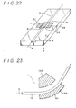
- FIG. 27 An example of the prior art cutoff type thin-film optical modulators is shown in Fig. 27.
- reference numeral 1 designates a substrate upon which an optical waveguide 2 is formed.
- Flat electrodes 3A and 3B are placed on both sides of a narrow portion as shown in Fig. 27 and in symmetrical relationship about the axis of the optical waveguide 2.
- An input prism coupler 5A is placed on the input end of the optical waveguide 2 in order to couple a light beam into the optical waveguide 2
- an output prism coupler 5B is placed on the output end of the optical waveguide 2 in order to receive the light beam propagated to the output end of the optical waveguide 2.
- a guided light beam is converted into a radiated light beam by electrically controlling the difference in refractive indices between the optical waveguide 2 and the substrate 1 underneath the waveguide 2 (in other words, the modulator is operated into the cutoff mode), so that it is difficult to achieve a sufficiently high light extinction ratio because of the following reasons:
- FIG. 1 A similar device with asymmetric electrode design as shown in Fig. 1 is disclosed in an article by D. Marcuse, in IEEE Journal of Quantum Electronics, Vol. QE-18, No. 3, March 1982, pp. 393-398, on which the two-part form of claim is based.
- the object of the present invention is to provide an optical element having a light extinction ratio higher than that by a prior art optical element.
- an optical element having an optical waveguide and flat electrodes arranged asymmetrically about said optical waveguide on a substrate in which an electric field can be applied through said flat electrodes to said substrate and said optical waveguide so that the refractive index of a portion of said substrate in the vicinity of said optical waveguide is varied to interrupt a light beam propagating through said optical waveguide, wherein impurities which alter the magnitude of the refractive index of said substrate are diffused in a portion under any one of said electrodes and a portion adjacent thereto.
- the optical waveguide may be straight.
- a first flat electrode of the flat electrodes may be spaced apart by a predetermined distance from one side edge of the optical waveguide or aligned with the one side edge of the optical waveguide.
- a second flat electrode of the flat electrodes may be spaced apart by a predetermined distance from the other side edge of the optical waveguide.
- a portion of the first flat electrode may be disposed on the optical waveguide; and one side edge of the first flat electrode may be in line with the one side edge of the optical waveguide or may be spaced apart therefrom by a predetermined distance.
- a third flat electrode of the flat electrodes may be disposed on the substrate and spaced apart by a predetermined distance from the first flat electrode on the side opposite to the second flat electrode with respect to the optical waveguide.
- the optical waveguide may have a curved portion.
- the first flat electrode may be disposed on the outer side of the optical waveguide in such a way that one side of the first flat electrode is aligned with the outer side edge of the curved portion of the optical waveguide or is spaced apart therefrom by a predetermined distance.
- the second flat electrode may be disposed on the inner side of the curved portion of the optical waveguide in such a way that the second flat electrode is spaced apart from the inner side edge of the curved portion of the optical waveguide by a predetermined distance.
- the optical waveguide may have a curved portion.
- the first flat electrode may have a portion overlying the optical waveguide and may be disposed on the inner side of the optical waveguide in such a way that one side edge of the flat electrode is aligned with the outer side edge of the curved portion of the optical waveguide or is spaced apart therefrom by a predetermined distance.
- the second flat electrode may be disposed on the outer side of the curved portion of the optical waveguide and may be spaced apart from the first flat electrode by a predetermined distance.
- the third flat electrode of the flat electrodes may be disposed on the inner side of the curved portion of the optical waveguide and may be spaced apart from the first flat electrode by a predetermined distance.
- the impurities in particular impurities for reducing a refractive index of the substrate can be diffused in a portion of the substrate between a portion adjacent to the one side edge of the optical waveguide and the second flat electrode, a portion under the second flat electrode and a portion adjacent thereto.
- Impurities for reducing a refractive index of the substrate can be diffused in a portion of the substrate under the first flat electrode and a portion of the substrate adjacent thereto.
- Impurities for increasing a refractive index of the substrate can be diffused into a portion of the substrate adjacent to the one side edge of the optical waveguide, a portion of the optical waveguide under the first flat electrode and a portion of the substrate adjacent thereto.
- Impurities for increasing a refractive index of the substrate can be diffused into a portion of the substrate between a portion adjacent to the one side edge of the optical waveguide and the second flat electrode, a portion of the substrate under the second flat electrode and a portion of the substrate adjacent thereto.
- reference numeral 1 designates a crystal which constitutes a substrate; 2, an optical waveguide formed on the substrate 1; and 3A and 3B, flat electrodes which are placed on both sides of the optical waveguide 2.
- One of the flat electrodes 3A and 3B (in the first embodiment 3A) is placed adjacent to the optical waveguide 2.
- Fig. 3 illustrates the dependence of the refractive index profile in the X-direction on an electric field applied to the optical waveguide 2 and the surface of the substrate 1 adjacent to the optical waveguide 2.
- the width of the optical waveguide 2 is 5 ⁇ m and the origin of the X-direction is located at the center of the optical waveguide 2.
- Fig. 3 shows that when a voltage is applied between the electrodes 3A and 3B, not only the refractive index profile in the direction of depth but also the refractive index profile in the X-direction exhibits asymmetry.
- the field intensity E(X) has a constant value, which is independent of X, between the electrodes and is zero under the electrodes.
- the refractive index of the substrate is 2.2.
- the difference between the refractive index at the surface of the optical waveguide and the refractive index of the substrate is 3 X 10 -3 .
- the thickness in the direction of depth of the optical waveguide is 2 ⁇ m.
- the wavelength of the incident light is 632.8 nm.
- the cutoff condition even for a single mode light wave is satisfied in the X-direction when a low electric field is applied.
- the width W of the optical waveguide is 4 ⁇ m
- the cutoff condition is satisfied with E(X) ⁇ 2 [V/ ⁇ m]. If the cutoff condition in the X-direction is satisfied, the effective refractive index (which determines a velocity of a light beam which propagates the optical waveguide) becomes lower than that of the substrate under the electrode, so that the confinement of the light beam within the optical waveguide is reduced and consequently the light beam radiates into the substrate under the electrode adjacent to the optical waveguide. This phenomenon is indicated by an arrow I in Fig. 2.
- the widths of the electrodes 3A and 3B placed on the both sides of the optical waveguide 2 may be equal to each other as shown in Fig. 2, but it is possible to make the width of the electrode 3A placed adjacent to the optical waveguide 2 larger or smaller than that of the electrode 3B.
- the optical modulation can be carried out.
- the difference between the electric field at the optical waveguide 2 and the electric field at the substrate 1 under the electrode is greater than the difference in other case. As a result, a higher light extinction rate can be obtained.
- the substrate 1 was made of a Y-cut LiNbO 3 (lithium niobate) crystal and Ti (titanium) was deposited 4 ⁇ m in width and 300 ⁇ in thickness and then heated for four hours in the air at 1000°C, whereby the straight optical waveguide 2 was formed.
- Aluminum electrodes 3A and 3B having a length of 4mm were formed on both sides of the optical waveguide 2 by a vacuum deposition method.
- the width of the electrode 3A adjacent to the optical waveguide 2 was 50 ⁇ m while the width of the electrode 3B was 2 mm.
- Reference numeral 1 designates a crystal which constitutes a susbstrate as in the case of the first embodiment and one electrode (for instance, 3A) is placed over an optical waveguide 2 in such a way that one side edges (the right sides in Fig. 6) of the optical waveguide 2 and the electrode 3A are aligned with each other.
- the mode of operation of the second embodiment will be described with reference to Fig. 7.
- the Y component E(Y) of the electric field just under the electrodes 3A and 3B becomes remarkably different from that of the electric field between the electrodes.
- the above-described phenomenon is utilized to change the refractive index of the optical waveguide 2 and the refractive indices of the substrates on both sides of the optical waveguide 2.
- a thin non-metallic film 6 with a refractive index lower than that of the optical waveguide 2 must be inserted as a buffer layer between the electrode 3A and the optical waveguide 2. Then, the light beam can be prevented from being absorbed by the metallic flat electrode 3A.
- the cutoff condition in the X-direction is satisfied by the application of an electric field; that is, when a refractive index of the optical waveguide 2 is reduced to a value very close to the refractive index of the substrate 1, the light beam is radiated into the substrate 1 between the electrodes 3A and 3B as indicated by an arrow II in Fig. 7.
- the distance between the electrodes 3A and 3B can be decreased so that the optical modulation or switching can be carried out at a lower voltage.
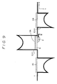
- the third embodiment is substantially similar in arrangement to the second embodiment as shown in Fig. 6 except that a third flat electrode 3C is placed in the vicinty of the flat electrode 3A in such a way that the electrodes 3B and 3C sandwich the electrode 3A.
- the mode of operation of the third embodiment is substantially similar to that of the second embodiment described above with reference to Fig. 6, but because the third flat electrode 3C induces another electric field, the Y component E(Y) of the applied electric field just under the flat electrode 3A becomes larger than that of the electric field established as shown in Fig. 6, so that the optical modulation can be carried out at a lower voltage.
- the profile of the refractive index becomes asymmetrical and the light wave radiates into the substrate as indicated by an arrow III.
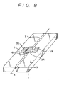
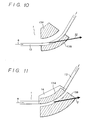
- An optical waveguide 12 having a curved portion is placed on a substrate 1 which is substantially similar to that as shown in Fig. 1 and an outer electrode 13B is placed adjacent to the curved portion of the optical waveguide 12, while an inner electrode 13A is placed on the opposite side of the optical waveguide 12 and is spaced apart therefrom by a predetermined distance.
- the two electrodes 13A and 13B are substantially in parallel with the optical waveguide 12.
- a light beam propagates straightly, so that the confinement of the light beam becomes weak in the curved portion of the optical waveguide 12.
- the optical element of the fourth embodiment can modulate a light beam at a light extinction ratio higher than that of the optical element as shown in Fig. 1.
- the propagating light beam is radiated into the substrate 1 under the electrode 13B as shown by an arrow IV in Fig. 10.
- Fig. 11 shows a fifth embodiment of the reference optical element.
- an optical waveguide 12 having a curved portion is placed on a substrate 1 which is substantially similar to that shown in Fig. 6.
- An inner electrode 13A is placed over the optical waveguide 12 in such a way that their outer arcuate sides are aligned with each other while the outer electrode 13B is spaced apart from the optical waveguide 12 by a predetermined distance.
- the two electrodes 13A and 13B are substantially in parallel with the optical waveguide 12.
- a buffer layer 16 is interposed between the electrode 13A and the optical waveguide 12.
- the confinement of a light beam within the optical waveguide 12 having the curved portion becomes weak, so that the optical modulation can be carried out at a light extinction ratio by far higher than that of the optical element as shown in Fig. 6.
- the propagating light beam is radiated into the substrate 1 between the electrodes 13A and 13B as indicated by an arrow V in Fig. 11.
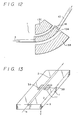
- Fig. 12 shows a sixth embodiment of the reference optical element which is substantially similar in arrangement to the fifth embodiment described above with reference to Fig. 11 except that a third flat electrode 13C is placed adjacent to and spaced apart by a predetermined distance from the electrode 13A radially inwardly in such a way that the third electrode 13C and the electrode 13B sandwich the flat electrode 13A.
- the mode of operation of the sixth embodiment is substantially similar to that of the optical element described with reference to Fig. 8. Due to the provision of the third flat electrode 13C, the electric field component in the direction perpendicular to the plane of Fig. 12 under the middle electrode 13A is increased as compared with the electric field component in the direction perpendicular to the plane of the optical element as shown in Fig. 11, so that the sixth embodiment can carry out the optical modulation at a voltage lower than a voltage which must be applied to the optical element as shown in Fig. 11.
- each of them comprises a substrate 1, an optical waveguide 2 or 12 and flat electrodes 3A, 3B and 3C or 13A, 13B and 13C, but it further comprises a substrate portion 11 or 21 into which no propagating light beam is radiated even in the cutoff mode and into which impurities are diffused so that a refractive index of the substrate 1 is decreased.
- the influence of the impurity diffusion upon the cutoff condition, in which the light beam radiates into the substrate 1, may be quantatively analyzed by using the effective index of refraction method.
- the effective index of refraction n f of this slab waveguide (The slab waveguide is described in detail by T. Tamir in "Integrated Optics", Springer Verlag, New York, 1975, p. 13) can be calculated by using the effective index of refraction method.
- the depth of the optical waveguide 2 is infinitely extended with keeping the width W unchanged.
- ⁇ n e represents a decrement in the refractive index of the substrate 1 when an electric field is applied and ⁇ n a represents a decrement in the refractive index of the substrate 1 due to the diffusion of impurities.
- E(X) at the intersection between H 4 and H represents a minimum field intensity required for cutting off a light beam and it is seen that the intersection is shifted to the side of lower field intensity in response to the increase in ⁇ n a .
- ⁇ n a is increased from 0 to 0.5x10 -3 , it is seen that the field intensity required for driving the optical element into the cutoff mode is 30% of the field intensity required for driving an optical element which is not diffused with impurities into the cutoff mode.
- optical elements having impurities thus diffused in accordance with the present invention are different from six types of embodiments described above in that a refractive index profile in the horizontal direction is made asymmetrical so that they can carry out the optical modulation at a voltage by far lower than a voltage required to drive the six embodiments with the same arrangements of the optical waveguide and electrodes.
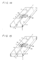
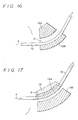
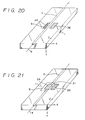
- optical elements as shown in Figs. 20, 21, 22, 23, 24 and 25 are substantially similar to the reference optical elements as shown in Figs. 1, 6, 8, 10, 11 and 12, respectively, in that each of them comprises a substrate 1, an optical waveguide 2 or 12 and flat electrodes 3A, 3B and 3C or 13A, 13B and 13C except that each of them is provided with a substrate portion 31 or 41 into which the propagating light beam is radiated in the cutoff mode and which is diffused with impurities so that a refractive index of the substrate portion 31 or 41 is increased.
- Fig. 26 shows the dependence of the normalized cutoff width H of the optical waveguide where a single-mode beam is radiated into the substrate 1 and the normalized width H 4 of the optical waveguide whose actual width is 4 ⁇ m upon the applied electric field in the case that the difference ⁇ n d between refractive indices of the surface of the optical waveguide and the substrate is 3x10 -3 .
- a parameter ⁇ n b indicates an increment in refractive index of the substrate due to the diffusion of impurities.
- Various conditions of Fig. 26 are the same as those of Fig. 4. As in the case of Fig. 19, the intersection of curve H and curve H 4 represents a minimum field intensity required for driving the optical element into the cutoff mode and it is seen that the higher the parameter ⁇ n b , the lower the applied electric field at which the optical element is driven into the cutoff mode becomes.
- the optical elements in accordance with the present invention have a double feature in that a refractive index profile of the substrate 1 in the horizontal direction is made asymmetrical due to the diffusion of impurities into the substrate 1 and that the normalized width of the optical waveguide is decreased. Therefore, as compared with the optical elements having the same arrangement of the optical waveguide and electrodes without impurities diffusion, the optical modulation can be carried out at a lower electric field.
- the optical modulation, optical switching or the like can be carried out by electrically controlling the difference between refractive indices of the optical waveguide and the substrate in the horizontal direction, so that the nonuniformity of the refractive index of the optical waveguide which causes some problems in conventional branching interference type optical modulator and directional optical coupler do not cause any problem in the present invention.
- an optical element in accordance with the present invention has a higher light extinction ratio and the output light is by far stabilized against the variation in temperature. Furthermore, in accordance with the present invention, light loss is smaller than that of the conventional device. A length of an optical element can be made less than one quarter or one third of those of the component parts in a conventional Mach-Zehnder type optical element and directional optical coupler. The fabrication of the optical element in accordance with the present invention is much facilitated.
- the optical element in accordance with the present invention has an extremely high light extinction ratio, so that it can be used as optical attenuator.
- optical attenuators Most of conventional optical attenuators have been utilizing the phenomenon that metal absorbs light and there has been devised and demonstrated an optical attenuator in which light is attenuated by varying the thickness of a thin metal film. However, it has some defects that it is too large in size and too heavy in weight and that the degree of attenuation is manually varied so that light cannot be attenuated at a higher rate.
- the optical element in accordance with the present invention has a ratio in optical intensity between the input and output lights is made higher than 56 dB so that the optical element can be satisfactorily used as high-speed optical attenuator which are compact in size and light in weight.
Landscapes
- Physics & Mathematics (AREA)
- Nonlinear Science (AREA)
- Chemical & Material Sciences (AREA)
- Engineering & Computer Science (AREA)
- Ceramic Engineering (AREA)
- Crystallography & Structural Chemistry (AREA)
- General Physics & Mathematics (AREA)
- Optics & Photonics (AREA)
- Optical Integrated Circuits (AREA)
Claims (10)
- Optisches Element mit einem optischen Wellenleiter (2, 12) und flachen Elektroden (3A, 3B, 3C, 13A, 13B, 13C), welche asymmetrisch um den optischen Wellenleiter (2, 12) auf einem Substrat (1) angeordnet sind, in welchem ein elektrisches Feld durch flache Elektroden (3A, 3B, 3C, 13A, 13B, 13C) auf das Substrat (1) und auf den optischen Wellenleiter (2, 12) einwirken kann, so daß der Brechungsindex eines Abschnitts des Substrats (1) in der Nähe des optischen Wellenleiters (2, 12) verändert wird, um einen Lichtstrahl zu unterbrechen, welcher sich durch den optischen Wellenleiter (2, 12) ausbreitet,
dadurch gekennzeichnet, daß Störstellen, welche die Größe des Brechungsindex des Substrats (1) verändern, in einen Abschnitt unter eine der Elektroden (3A, 3B, 3C, 13A, 13B, 13C) und einen dazu benachbarten Abschnitt diffundieren. - Optisches Element nach Anspruch 1, wobei der optische Wellenleiter (2, 12) gerade ist,eine erste flache Elektrode (3A, 13A) der flachen Elektroden (3A, 3B, 3C, 13A, 13B, 13C) um einen vorbestimmten Abstand von einer Seitenkante des optischen Wellenleiters (2, 12) beabstandet ist, undeine zweite flache Elektrode (3B, 13B) der flachen Elektroden (3A, 3B, 3C, 13A, 13B, 13C) um einen vorbestimmten Abstand von der anderen Seitenkante des optischen Wellenleiters (2, 12) beabstandet ist.
- Optisches Element gemäß Anspruch 1, wobei der optische Wellenleiter (2, 12) gerade ist,eine Seitenkante einer ersten flachen Elektrode (3A, 13A) der flachen Elektroden (3A, 3B, 3C, 13A, 13B, 13C) in Linie mit einer Seitenkante des optischen Wellenleiters (2, 12) ist, undeine zweite flache Elektrode (3B, 13B) der flachen Elektroden (3A, 3B, 3C, 13A, 13B, 13C) um einen vorbestimmten Abstand von der anderen Seitenkante des optischen Wellenleiters (2, 12) beabstandet ist.
- Optisches Element gemäß Anspruch 1, wobei ein Abschnitt einer ersten flachen Elektrode (3A, 13A) der flachen Elektroden (3A, 3B, 3C, 13A, 13B, 13C) auf dem optischen Wellenleiter (2, 12) angeordnet ist, und eine Seitenkante der ersten flachen Elektrode (3A, 13A) in Linie mit einer Seitenkante des optischen Wellenleiters (2, 12) ist, wobei eine Pufferschicht (6) zwischen der ersten Elektrode (3A, 13A) und dem optischen Wellenleiter (2, 12) angeordnet ist, und eine zweite flache Elektrode (3B, 13B) der flachen Elektroden (3A, 3B, 3C, 13A, 13B, 13C) um einen vorbestimmten Abstand von der Seitenkante des optischen Wellenleiters (2, 12) beabstandet ist.
- Optisches Element gemäß Anspruch 1, wobei ein Abschnitt einer ersten flachen Elektrode (3a, 13A) auf dem optischen Wellenleiter (2, 12) angeordnet ist, undeine Seitenkante der ersten flachen Elektrode (3A, 13A) von einer Seitenkante des optischen Wellenleiters (2, 12) um einen vorbestimmten Abstand beabstandet ist, wobei eine Pufferschicht (6) zwischen der erste Elektrode (3A, 13A) und dem optischen Wellenleiter (2, 12) angeordnet ist, undeine zweite flache Elektrode (3B, 13B) der flachen Elektroden (3A, 3B, 3C, 13A, 13B, 13C) um einen vorbestimmten Abstand von der Seitenkante des optischen Wellenleiters (2, 12) beabstandet ist.
- Optisches Element gemäß Anspruch 2 bis 5, wobei eine dritte flache Elektrode (3C, 13C) der flachen Elektroden (3A, 3B, 3C, 13A, 13B, 13C) auf dem Substrat (1) angeordnet ist und um einen vorbestimmten Abstand von der ersten flachen Elektrode (3A, 13A) auf der Seite in Gegenüberlage zu der zweiten flachen Elektrode (3B, 13B) mit Bezug zu dem optischen Wellenleiter (2, 12) beabstandet ist.
- Optisches Element gemäß Anspruch 2 bis 6, wobei Störstellen, welche die Größe eines Brechungsindex des Substrats (1) verändern, in einen Abschnitt (11) des Substrats (1) zwischen einem Abschnitt in unmittelbarer Nähe zu einer Seitenkante des Wellenleiters (2, 12) und der zweiten flachen Elektrode (3B, 13B), einen Abschnitt unter der zweiten flachen Elektrode (3B, 13B) und einen dazu benachbarten Abschnitt diffundieren.
- Optisches Element gemäß Anspruch 2 bis 6, wobei die Störstellen, welche die Größe eines Brechungsindex des Substrats (1) verändern, in einen Abschnitt (21) des Substrats (1) unter der ersten flachen Elektrode (3A, 13A) und einen dazu benachbarten Abschnitt des Substrats diffundieren.
- Optisches Element gemäß Anspruch 2 bis 6, wobei die Störstellen, welche die Größe eines Brechungsindex des Substrats (1) verändern, in einen Abschnitt (21) des Substrats (1) in unmittelbarer Nähe einer Seitenkante des optischen Wellenleiters (2, 12), einen Abschnitt des optischen Wellenleiters (2, 12) unter der ersten flachen Elektrode (3A, 13A) und einen dazu benachbarten Abschnitt des Substrats (1) diffundieren.
- Optisches Element gemäß Anspruch 2 bis 6, wobei die Störstellen, welche die Größe eines Brechungsindex des Substrats (1) verändern, in einen Abschnitt (11) des Substrats (1) zwischen einem Abschnitt in unmittelbarer Nähe einer Seitenkante des optischen Wellenleiters (2, 12) und der zweiten flachen Elektrode (3b, 13B), einen Abschnitt des Substrats (1) und einen dazu benachbarten Abschnitt des Substrats diffundieren.
Applications Claiming Priority (3)
| Application Number | Priority Date | Filing Date | Title |
|---|---|---|---|
| JP60051837A JPH0627914B2 (ja) | 1985-03-15 | 1985-03-15 | 光学素子 |
| JP51837/85 | 1985-03-15 | ||
| EP86103304A EP0201684B1 (de) | 1985-03-15 | 1986-03-12 | Elektrooptischer Welleneleitermodulator |
Related Parent Applications (1)
| Application Number | Title | Priority Date | Filing Date |
|---|---|---|---|
| EP86103304.1 Division | 1986-03-12 |
Publications (3)
| Publication Number | Publication Date |
|---|---|
| EP0443636A2 EP0443636A2 (de) | 1991-08-28 |
| EP0443636A3 EP0443636A3 (en) | 1992-03-25 |
| EP0443636B1 true EP0443636B1 (de) | 1996-06-05 |
Family
ID=12897971
Family Applications (2)
| Application Number | Title | Priority Date | Filing Date |
|---|---|---|---|
| EP86103304A Expired - Lifetime EP0201684B1 (de) | 1985-03-15 | 1986-03-12 | Elektrooptischer Welleneleitermodulator |
| EP91106032A Expired - Lifetime EP0443636B1 (de) | 1985-03-15 | 1986-03-12 | Optisches Element |
Family Applications Before (1)
| Application Number | Title | Priority Date | Filing Date |
|---|---|---|---|
| EP86103304A Expired - Lifetime EP0201684B1 (de) | 1985-03-15 | 1986-03-12 | Elektrooptischer Welleneleitermodulator |
Country Status (4)
| Country | Link |
|---|---|
| US (1) | US4818063A (de) |
| EP (2) | EP0201684B1 (de) |
| JP (1) | JPH0627914B2 (de) |
| DE (2) | DE3687920T2 (de) |
Families Citing this family (20)
| Publication number | Priority date | Publication date | Assignee | Title |
|---|---|---|---|---|
| GB2193337B (en) * | 1986-07-30 | 1990-03-07 | Gen Electric Plc | Optical switch apparatus |
| FR2615006B1 (fr) * | 1987-05-04 | 1991-10-04 | Thomson Csf | Guide d'onde optique integre, son procede de fabrication, et son utilisation dans un modulateur electro-optique |
| JPH0711607B2 (ja) * | 1988-03-03 | 1995-02-08 | 沖電気工業株式会社 | 光曲げ導波路 |
| US4934775A (en) * | 1989-01-18 | 1990-06-19 | Gte Laboratories Incorporated | Optical space switches using cascaded coupled-waveguide optical gate arrays |
| US5153930A (en) * | 1990-01-04 | 1992-10-06 | Smiths Industries Aerospace & Defense Systems, Inc. | Device employing a substrate of a material that exhibits the pyroelectric effect |
| US5050948A (en) * | 1990-08-23 | 1991-09-24 | Tektronix, Inc. | Traveling wave electro-optic modulator |
| JP2758538B2 (ja) * | 1992-09-28 | 1998-05-28 | 松下電器産業株式会社 | 光変調素子と光変調装置及びその駆動方法 |
| KR100261230B1 (ko) * | 1997-07-14 | 2000-07-01 | 윤종용 | 집적광학 광 강도 변조기 및 그 제조방법 |
| DE19816674A1 (de) * | 1998-04-15 | 1999-10-28 | Fraunhofer Ges Forschung | Optisches Bauelement und Verfahren zum Schalten oder Modulieren von Licht |
| KR100288447B1 (ko) | 1998-06-26 | 2001-06-01 | 윤종용 | 광강도변조기및그제조방법 |
| US7013053B2 (en) * | 2000-01-24 | 2006-03-14 | Ramot At Tel Aviv University Ltd. | Polarization independent electro-optical device for modulation of light |
| GB0002277D0 (en) | 2000-02-01 | 2000-03-22 | Sdl Integrated Optics Ltd | Intergrated optical components |
| US6424754B1 (en) * | 2000-09-29 | 2002-07-23 | Tasc, Inc. | Optical modulator responsive to at least two electric signals |
| US7035524B2 (en) * | 2002-12-26 | 2006-04-25 | Fujitsu Limited | Variable optical attenuator |
| JP2004287093A (ja) * | 2003-03-20 | 2004-10-14 | Fujitsu Ltd | 光導波路、光デバイスおよび光導波路の製造方法 |
| EP2024190B9 (de) * | 2006-06-06 | 2012-09-05 | Hydro Aluminium Rolled Products GmbH | Verfahren zur konditionierung der oberfläche eines lithobands |
| WO2009096237A1 (ja) * | 2008-01-31 | 2009-08-06 | Ngk Insulators, Ltd. | 光導波路デバイス |
| JP5012624B2 (ja) * | 2008-03-31 | 2012-08-29 | 住友大阪セメント株式会社 | 光導波路素子 |
| JP2013047627A (ja) * | 2011-08-29 | 2013-03-07 | Toyota Industries Corp | 光導波路型電圧センサ |
| FR3027414B1 (fr) * | 2014-10-15 | 2017-11-10 | Photline Tech | Modulateur de phase electrooptique et procede de modulation |
Family Cites Families (8)
| Publication number | Priority date | Publication date | Assignee | Title |
|---|---|---|---|---|
| US3804489A (en) * | 1972-12-06 | 1974-04-16 | Bell Telephone Labor Inc | Electro-optic thin-film diffraction loss modulator |
| US4142775A (en) * | 1976-09-27 | 1979-03-06 | Bell Telephone Laboratories, Incorporated | Optical signal processing devices |
| US4291939A (en) * | 1978-03-24 | 1981-09-29 | The United States Of America As Represented By The Secretary Of The Navy | Polarization-independent optical switches/modulators |
| JPS559534A (en) * | 1978-07-07 | 1980-01-23 | Nippon Telegr & Teleph Corp <Ntt> | Optical fiber device |
| US4262993A (en) * | 1980-01-11 | 1981-04-21 | The United States Of America As Represented By The Secretary Of The Navy | Electrooptically balanced alternating Δβ switch |
| JPS5744128A (en) * | 1980-08-29 | 1982-03-12 | Nec Corp | Optical deflector |
| US4390236A (en) * | 1981-03-19 | 1983-06-28 | Bell Telephone Laboratories, Incorporated | Tunable polarization independent wavelength filter |
| FR2528991A1 (fr) * | 1982-06-22 | 1983-12-23 | Thomson Csf | Dispositif optique integre modulateur independant de la polarisation incidente |
-
1985
- 1985-03-15 JP JP60051837A patent/JPH0627914B2/ja not_active Expired - Lifetime
-
1986
- 1986-03-03 US US06/835,284 patent/US4818063A/en not_active Expired - Lifetime
- 1986-03-12 EP EP86103304A patent/EP0201684B1/de not_active Expired - Lifetime
- 1986-03-12 DE DE8686103304T patent/DE3687920T2/de not_active Expired - Fee Related
- 1986-03-12 EP EP91106032A patent/EP0443636B1/de not_active Expired - Lifetime
- 1986-03-12 DE DE3650529T patent/DE3650529T2/de not_active Expired - Fee Related
Also Published As
| Publication number | Publication date |
|---|---|
| EP0443636A2 (de) | 1991-08-28 |
| EP0201684B1 (de) | 1993-03-10 |
| EP0201684A3 (en) | 1988-03-30 |
| EP0201684A2 (de) | 1986-11-20 |
| DE3687920T2 (de) | 1993-07-01 |
| DE3687920D1 (de) | 1993-04-15 |
| JPH0627914B2 (ja) | 1994-04-13 |
| EP0443636A3 (en) | 1992-03-25 |
| JPS61210321A (ja) | 1986-09-18 |
| DE3650529T2 (de) | 1996-11-21 |
| US4818063A (en) | 1989-04-04 |
| DE3650529D1 (de) | 1996-07-11 |
Similar Documents
| Publication | Publication Date | Title |
|---|---|---|
| EP0443636B1 (de) | Optisches Element | |
| US5566257A (en) | Electro-optic modulator | |
| US4709978A (en) | Mach-Zehnder integrated optical modulator | |
| US4866406A (en) | Wide-band optical modulator | |
| US4130342A (en) | Passive optical channel crossover, switch and bend structure | |
| US4983006A (en) | Polarization-independent optical waveguide switch | |
| EP0618464A1 (de) | Polarisationsteiler | |
| EP1892559A2 (de) | Geräte mit optischen Funktionen | |
| WO2003102676A1 (en) | Electro-optic modulators | |
| US7079714B2 (en) | Electro-optic devices having flattened frequency response with reduced drive voltage | |
| Thaniyavarn | Wavelength independent, optical damage immune Z‐propagation LiNbO3 waveguide polarization converter | |
| US4561718A (en) | Photoelastic effect optical waveguides | |
| Hui et al. | Electrode optimization for high-speed traveling-wave integrated optic modulators | |
| EP0425991B1 (de) | Optischer Wellenleiterschalter | |
| US7912325B2 (en) | Optical control element | |
| US7088874B2 (en) | Electro-optic devices, including modulators and switches | |
| Goel et al. | Design considerations for low switching voltage crossing channel switches | |
| Khan et al. | Technique for velocity-matched traveling-wave electrooptic modulator in AlGaAs/GaAs | |
| EP0417295B1 (de) | Verfahren und vorrichtung für fernsehrundfunk | |
| US7013053B2 (en) | Polarization independent electro-optical device for modulation of light | |
| Wooten et al. | Test structures for characterization of electrooptic waveguide modulators in lithium niobate | |
| US4199221A (en) | Electro-optic thin-film waveguide modulator device | |
| US5815609A (en) | Waveguide type optical external modulator | |
| US20020181822A1 (en) | Reduced power consumption thermo-optic devices | |
| JP3119965B2 (ja) | 光導波路型光素子 |
Legal Events
| Date | Code | Title | Description |
|---|---|---|---|
| PUAI | Public reference made under article 153(3) epc to a published international application that has entered the european phase |
Free format text: ORIGINAL CODE: 0009012 |
|
| AC | Divisional application: reference to earlier application |
Ref document number: 201684 Country of ref document: EP |
|
| AK | Designated contracting states |
Kind code of ref document: A2 Designated state(s): DE FR GB |
|
| PUAL | Search report despatched |
Free format text: ORIGINAL CODE: 0009013 |
|
| AK | Designated contracting states |
Kind code of ref document: A3 Designated state(s): DE FR GB |
|
| 17P | Request for examination filed |
Effective date: 19920427 |
|
| 17Q | First examination report despatched |
Effective date: 19940125 |
|
| GRAH | Despatch of communication of intention to grant a patent |
Free format text: ORIGINAL CODE: EPIDOS IGRA |
|
| GRAA | (expected) grant |
Free format text: ORIGINAL CODE: 0009210 |
|
| AC | Divisional application: reference to earlier application |
Ref document number: 201684 Country of ref document: EP |
|
| AK | Designated contracting states |
Kind code of ref document: B1 Designated state(s): DE FR GB |
|
| REF | Corresponds to: |
Ref document number: 3650529 Country of ref document: DE Date of ref document: 19960711 |
|
| ET | Fr: translation filed | ||
| PLBE | No opposition filed within time limit |
Free format text: ORIGINAL CODE: 0009261 |
|
| STAA | Information on the status of an ep patent application or granted ep patent |
Free format text: STATUS: NO OPPOSITION FILED WITHIN TIME LIMIT |
|
| 26N | No opposition filed | ||
| PGFP | Annual fee paid to national office [announced via postgrant information from national office to epo] |
Ref country code: DE Payment date: 20010306 Year of fee payment: 16 |
|
| PGFP | Annual fee paid to national office [announced via postgrant information from national office to epo] |
Ref country code: GB Payment date: 20010307 Year of fee payment: 16 |
|
| PGFP | Annual fee paid to national office [announced via postgrant information from national office to epo] |
Ref country code: FR Payment date: 20010313 Year of fee payment: 16 |
|
| REG | Reference to a national code |
Ref country code: GB Ref legal event code: IF02 |
|
| PG25 | Lapsed in a contracting state [announced via postgrant information from national office to epo] |
Ref country code: GB Free format text: LAPSE BECAUSE OF NON-PAYMENT OF DUE FEES Effective date: 20020312 |
|
| PG25 | Lapsed in a contracting state [announced via postgrant information from national office to epo] |
Ref country code: DE Free format text: LAPSE BECAUSE OF NON-PAYMENT OF DUE FEES Effective date: 20021001 |
|
| GBPC | Gb: european patent ceased through non-payment of renewal fee |
Effective date: 20020312 |
|
| PG25 | Lapsed in a contracting state [announced via postgrant information from national office to epo] |
Ref country code: FR Free format text: LAPSE BECAUSE OF NON-PAYMENT OF DUE FEES Effective date: 20021129 |
|
| REG | Reference to a national code |
Ref country code: FR Ref legal event code: ST |