EP0443800A2 - A charging method and a charging device - Google Patents
A charging method and a charging device Download PDFInfo
- Publication number
- EP0443800A2 EP0443800A2 EP91301275A EP91301275A EP0443800A2 EP 0443800 A2 EP0443800 A2 EP 0443800A2 EP 91301275 A EP91301275 A EP 91301275A EP 91301275 A EP91301275 A EP 91301275A EP 0443800 A2 EP0443800 A2 EP 0443800A2
- Authority
- EP
- European Patent Office
- Prior art keywords
- charging
- voltage
- charged
- photosensitive drum
- charging roller
- Prior art date
- Legal status (The legal status is an assumption and is not a legal conclusion. Google has not performed a legal analysis and makes no representation as to the accuracy of the status listed.)
- Granted
Links
- 238000000034 method Methods 0.000 title claims description 3
- 125000006850 spacer group Chemical group 0.000 abstract description 15
- 238000004519 manufacturing process Methods 0.000 description 8
- 229910052751 metal Inorganic materials 0.000 description 7
- 239000002184 metal Substances 0.000 description 7
- 238000012546 transfer Methods 0.000 description 7
- 229920002943 EPDM rubber Polymers 0.000 description 5
- 239000000463 material Substances 0.000 description 5
- OKTJSMMVPCPJKN-UHFFFAOYSA-N Carbon Chemical compound [C] OKTJSMMVPCPJKN-UHFFFAOYSA-N 0.000 description 2
- CBENFWSGALASAD-UHFFFAOYSA-N Ozone Chemical compound [O-][O+]=O CBENFWSGALASAD-UHFFFAOYSA-N 0.000 description 2
- 229910000831 Steel Inorganic materials 0.000 description 2
- 229910052782 aluminium Inorganic materials 0.000 description 2
- XAGFODPZIPBFFR-UHFFFAOYSA-N aluminium Chemical compound [Al] XAGFODPZIPBFFR-UHFFFAOYSA-N 0.000 description 2
- 229910052799 carbon Inorganic materials 0.000 description 2
- 238000002474 experimental method Methods 0.000 description 2
- 230000002093 peripheral effect Effects 0.000 description 2
- 239000004014 plasticizer Substances 0.000 description 2
- 239000010959 steel Substances 0.000 description 2
- 239000004677 Nylon Substances 0.000 description 1
- 239000004809 Teflon Substances 0.000 description 1
- 229920006362 Teflon® Polymers 0.000 description 1
- 230000009471 action Effects 0.000 description 1
- 230000015572 biosynthetic process Effects 0.000 description 1
- 230000015556 catabolic process Effects 0.000 description 1
- 238000004140 cleaning Methods 0.000 description 1
- 239000004020 conductor Substances 0.000 description 1
- 230000007547 defect Effects 0.000 description 1
- 238000011156 evaluation Methods 0.000 description 1
- 238000009413 insulation Methods 0.000 description 1
- 239000004973 liquid crystal related substance Substances 0.000 description 1
- 230000007246 mechanism Effects 0.000 description 1
- 238000012986 modification Methods 0.000 description 1
- 230000004048 modification Effects 0.000 description 1
- 229920001778 nylon Polymers 0.000 description 1
- 230000008569 process Effects 0.000 description 1
- 229910001220 stainless steel Inorganic materials 0.000 description 1
- 239000010935 stainless steel Substances 0.000 description 1
Images

Classifications
-
- G—PHYSICS
- G03—PHOTOGRAPHY; CINEMATOGRAPHY; ANALOGOUS TECHNIQUES USING WAVES OTHER THAN OPTICAL WAVES; ELECTROGRAPHY; HOLOGRAPHY
- G03G—ELECTROGRAPHY; ELECTROPHOTOGRAPHY; MAGNETOGRAPHY
- G03G15/00—Apparatus for electrographic processes using a charge pattern
- G03G15/02—Apparatus for electrographic processes using a charge pattern for laying down a uniform charge, e.g. for sensitising; Corona discharge devices
- G03G15/0208—Apparatus for electrographic processes using a charge pattern for laying down a uniform charge, e.g. for sensitising; Corona discharge devices by contact, friction or induction, e.g. liquid charging apparatus
- G03G15/025—Apparatus for electrographic processes using a charge pattern for laying down a uniform charge, e.g. for sensitising; Corona discharge devices by contact, friction or induction, e.g. liquid charging apparatus by bringing a charging member in the vicinity with the member to be charged, e.g. proximity charging, forming microgap
Definitions
- the present invention relates to a charging device usable with an image forming apparatus such as an electrophotographic machine or an electrostatic recording machine, in which a member to be charged such as a photosensitive member or a dielectric member is uniformly charged or discharged.
- a corona discharger such as a corotron or scorotron is widely used since the uniformity of the charging is sufficiently provided.
- corona dischargers involve the drawbacks that it requires an expensive high voltage source, that it requires much space therefor and for the shield for the high voltage source or the like, that the production of ozone is relatively large, which requires means against the production and larger size of the device and a higher cost.
- a charging member is contacted to the member to be charged such as the image bearing member, while the charging member is supplied with a voltage which may be a DC voltage of 1 - 2 Kv or a DC biased AC voltage, by which the member to be charged is charged to a predetermined polarity.
- a voltage which may be a DC voltage of 1 - 2 Kv or a DC biased AC voltage, by which the member to be charged is charged to a predetermined polarity.
- the contact type charging has the advantages that it is possible to lower the voltage of the voltage source, that the production of ozone is very slight, if any, the structure is simple with a small size, that the cost is low, and the like.
- the image forming apparatus comprises an electrophotographic photosensitive member 1, which will hereinafter be called “photosensitive drum”, and which is rotated in a direction A indicated by an arrow at a predetermined peripheral speed (process speed).
- a charging roller 20 is the charging member, and comprises a conductive core (shaft) 20a made of steel or stainless steel or the like, and an outer layer 20b, thereon, made of EPDM or the like containing carbon to provide a predetermined low resistance.
- the charging roller 20 is supported by bearings at the opposite longitudinal ends of the core metal 20a fro free rotation, and in parallelism with the generating line of the photosensitive drum 1. It is urged to the photosensitive drum 1 with a predetermined pressure so that it rotates following the rotation of the photosensitive drum 1.
- the apparatus further comprises an external voltage source to the charging roller 20.
- the voltage which is a sum of a DC voltage and an AC voltage having a peak-to-peak voltage which is not less than the charge starting voltage between the charging roller 20 and the photosensitive layer.
- the voltage is supplied to the charging roller 20 through sliding contacts 8 contacted to the ends of the core metal 20a.
- the surface of the photosensitive drum 1 is sequentially charged by the charging roller 20 which is supplied with such a voltage and which is contacted to the surface to a predetermined potential of a predetermined polarity.
- the uniformly charged surface of the rotating photosensitive drum 1 thus uniformly charged is exposed to image light 3 bearing the intended image formation (print information) through an unshown exposure means such as analog exposure means fot an original document, a laser scanner, LED array, liquid crystal shutter array, or the like through a slit or by way of scanning means. By doing so, an electrostatic latent image of the intended information is formed sequentially on the surface of the rotating photosensitive drum 1.
- the thus formed electrostatic latent image is developed by a developing device (developing roller) 4 into a toner image, which is in turn transferred onto a transfer material 7 at an image transfer station between the photosensitive drum 1 and a transfer roller 5 supplied with an image transfer bias voltage.
- the transfer material 7 is fed from unshown feeding mechanism at a predetermined timing in association with the image on the photosensitive drum 1.
- the transfer material 7 now having received the toner image is separated from the surface of the photosensitive drum 1, and is introduced into an image fixing apparatus where the toner image is fixed thereon.
- the surface of the photosensitive drum after the image transfer is cleaned by a cleaner so that the residual toner or the like is removed therefrom, and the photosensitive drum 1 is prepared for the next image forming operation.
- the outer layer 20a of the charging roller 20 is made of EPDM, for example, as described above.
- the EPDM material is contacted to the surface of the photosensitive drum 1 which is the member to be charged.
- Plasticizer contained in the EPDM may oozes out thereof and may be transferred to the surface of the photosensitive drum 1 during the period in which the photosensitive drum 1 is not rotated, with the result of tracks of the roller on the photosensitive drum 1. This deteriorates the image quality.
- the charging roller When the AC voltage is applied to the charging roller contacted to the photosensitive drum, the charging roller may vibrate with the result of noise (charging noise).
- Figure 1 is a sectional view of an image forming apparatus according to an embodiment of the present invention.
- FIG 2 is a front view of a charging device used in the image forming apparatus of Figure 1.
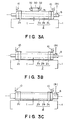
- FIGS. 3A, 3B and 3C are sectional views of charging devices according to other embodiments of the present invention having different roller warp preventing means.
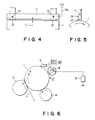
- Figure 4 is a front view according to a further embodiment of the present invention using a charging blade.
- Figure 5 is a side view thereof.
- Figure 6 is a sectional view of an image forming apparatus using a contact type charging device.
- FIG 1 there is shown an exemplary image forming apparatus using a proximity (non-contact) type charging device for uniformly charging an image bearing member.
- Figure 2 is front view of the part adjacent the charging device.
- the photosensitive drum 1 of this embodiment comprises an aluminum base 1b and a photosensitive layer 1a on the outer surface of the base 1b, which is made of organic photoconductor (OPC).
- OPC organic photoconductor
- the photosensitive drum 1 has an outer diameter of 30 mm.
- the charging roller is designated by a reference numeral 2. It comprises a conductive core (shaft) 2a of aluminum, steel or the like, an outer layer 2b of EPDM or the like having a resistance lowered by addition of carbon or the like to a predetermined level, and a spacer ring layers 2c and 2c of nylon, teflon or the like mounted on the outer layer 2b along the circumferential periphery thereof at the longitudinal opposite ends.
- the charging roller 2 is supported by unshown bearings at the longitudinal opposite ends of the core metal 2a to be substantially parallel with the generating line of the photosensitive drum 1.
- the charging roller 2 is confined by urging means 10 and 10 such as springs adjacent the opposite ends of the charging roller 2, so that the charging roller 2 is pressed to the photosensitive drum 1 at the spacer ring layers 2c and 2c at a predetermined pressure.
- the portion of the charging roller 2 between the spacer layers 2c and 2c is maintained out of contact from the photosensitive drum 1 with a clearance t, corresponding to the thickness of the spacer ring layer 2c and 2c.
- the charging roller 2 may be rotated following the rotation of the photosensitive drum 1 or may be positively driven codirectionally with the photosensitive drum 1, or it may be rotated in the opposite direction, or it may be unrotated.
- the charging roller is supplied with an oscillating voltage (the voltage level periodically changes with time) having a waveform provided by biasing an AC voltage with a DC voltage, through sliding contacts 8 contacted to the ends of the core metal 2a.
- the uniform charging is accomplished by such a voltage setting that a charge starting voltage V TH when only a DC voltage is applied to the charging roller and the peak-to-peak voltage Vpp of the AC voltage component of applied voltage satisfy Vpp ⁇ 2 V TH .
- the charge starting voltage is determined in the following manner. Only DC component is applied to the charging member contacted to the image bearing member (photosensitive member) having a zero surface potential. the voltage of the DC component is gradually increased. the surface potentials of the photosensitive member are plotted with respect to the DC voltage applied thereto with a predetermined increment of the voltage, for example, 100 volts. The first point of the voltage is the one at which the surface potential of the photosensitive member appears, and about ten surface potential are plotted at each 100 volt increment, for example. Using least square approximatrion, a straight line is drawn from the plots. the DC voltage reading at which the straight line and the line representing the zero surface potential as the charge starting voltage. The waveform may be rectangular, triangular, pulsewise or simple DC form.
- the charging operation has been performed with the following conditions: the clearance t between the central portion of the charging roller 2 and the photosensitive drum 1 by the spacer ring layer 2c and 2c: 30 microns the peripheral speed of the photosensitive drum 1: 15 ⁇ mm/sec the voltages supplied to the charging roller 2 from the voltage source 9: DC of -700 V, and AC of 1500V and 255 Hz.
- the following table shows the results of the experiments where the clearance t is changed by the spacer ring layer 2c and 2c from 1 micron to 500 microns.
- the pits and projections of the charging roller surface are partly in contact with the surface of the photosensitive drum. Therefore, when an external bias is applied to the charging roller, the charging noise is produced. If it is not less than 5 microns, the charging roller is out of contact with the photosensiitive drum, and therefore, the charging noise is not produced.
- G means no production of the charging noise
- S means slight production of the charging noise
- N means production of the charging noise.
- the charging roller In the structure where the charging roller is urged to the photosensitive drum adjacent the opposite ends of the charging roller 2 by urging means 10 and 10, and is contacted to the photosensitive drum at the spacer ring layer 2c and 2c, if the urging force by the urging means is too strong, the charging roller 2 may be warped between the spacer ring layer 2c and 2c in the upward direction, with the result of the larger clearance between the central portion of the charging roller and the photosensitive drum than the clearance defined by the spacer ring layer 2c and 2c.
- the thickness of the spacer ring layer 2c and 2c is set to 300 microns, it is possible that the clearance between the central portion of the charging roller and the photosensitive drum is larger than the tolerable 300 microns due the warping of the charging roller.
- FIGS 3A, 3B and 3C show the measures against this.
- a confining roller 30 is disposed in the middle of the charging roller 2 to prevent the warping.
- the roller 30 is supported on the shaft 31, and the roller 32 is urged by a spring 32 to the charging roller 2.
- the charging roller 2 tends to warp upwardly due to too strong forces by the urging means 10 and 10 with the result of the tendency of warping of the charging roller in the middle region.
- the tendency is suppressed so that the clearance t is between the charging roller 2 and the photosensitive drum 1 is maintained at the level corresponding to the thickness of the spacer ring layer 2c and 2c.
- Figure 3B shows an example in which the core metal 2a of the charging roller 2 has a diameter which is larger at the central portion than at the longitudinal end portions to suppress the warping of the charging roller 2 at the middle portion.
- the diameter of the core metal 2a is uniformly increased to such an extent that the warping of the charging roller does not occur.
- the material cost increases corresponding to the increase of the diameter.
- the since the core metal is a straight roller so that it is easy to polish. Totally, this example is low in cost.
- the charging member is in the form of a blade.
- a charging blade 11 is made of conductive material.
- the longitudinal end portions of the charging blade is mounted on spacer members 12 and 12 by screws 13 and 13.
- the spacer members 12 and 12 are supported on a stationary member not shown.
- the clearance t between the charging blade 11 and the photosensitive drum 1 is defined by the spacer members 12 and 12.
- the voltage is supplied to the charging blade 11 from the voltage source directly through a lead wires 9a.
- the charging member 11 is not movable, so that the electric noise due to the electric contacts can be suppressed.
- the required space is smaller than in the charging roller. because the necessity for the confining of the charging member by the urging means as in the case of the charging roller, can be eliminated. Therefore, the problem of the warping is avoided.
- the proximity type charging device of the present invention substantially maintains the advantages of the contact type charging roller, and additionally advantageous in that tracks of the charging device and the charging noise as produced in the contact type charging device can be avoided.
Landscapes
- Physics & Mathematics (AREA)
- Engineering & Computer Science (AREA)
- Plasma & Fusion (AREA)
- General Physics & Mathematics (AREA)
- Electrostatic Charge, Transfer And Separation In Electrography (AREA)
Abstract
Description
- The present invention relates to a charging device usable with an image forming apparatus such as an electrophotographic machine or an electrostatic recording machine, in which a member to be charged such as a photosensitive member or a dielectric member is uniformly charged or discharged.
- As for means for uniformly charging the member to be charged such as the image bearing member to a predetermined potential of a predetermined polarity, a corona discharger such as a corotron or scorotron is widely used since the uniformity of the charging is sufficiently provided.
- However, the corona dischargers involve the drawbacks that it requires an expensive high voltage source, that it requires much space therefor and for the shield for the high voltage source or the like, that the production of ozone is relatively large, which requires means against the production and larger size of the device and a higher cost.
- Recently, therefore, the consideration is made as to the contact type charging device and apparatus in place of the corona discharger involving the above problems.
- In the contact type system, a charging member is contacted to the member to be charged such as the image bearing member, while the charging member is supplied with a voltage which may be a DC voltage of 1 - 2 Kv or a DC biased AC voltage, by which the member to be charged is charged to a predetermined polarity. It includes a roller charging type (Japanese Laid-open Patent Application No. 91253/1981), blade charging type (Japanese Laid-open Patent Applications Nos. 194349/1981 and 147756/1985), charging and cleaning type (Japanese Laid-open Patent Application No. 165166/1981).
- The contact type charging has the advantages that it is possible to lower the voltage of the voltage source, that the production of ozone is very slight, if any, the structure is simple with a small size, that the cost is low, and the like.
- Referring to Figure 6, there is shown an example of an image forming apparatus having such a contact type charging device for uniformly charging the surface of the image forming apparatus. The image forming apparatus comprises an electrophotographic photosensitive member 1, which will hereinafter be called "photosensitive drum", and which is rotated in a direction A indicated by an arrow at a predetermined peripheral speed (process speed).
- A
charging roller 20 is the charging member, and comprises a conductive core (shaft) 20a made of steel or stainless steel or the like, and anouter layer 20b, thereon, made of EPDM or the like containing carbon to provide a predetermined low resistance. Thecharging roller 20 is supported by bearings at the opposite longitudinal ends of the core metal 20a fro free rotation, and in parallelism with the generating line of the photosensitive drum 1. It is urged to the photosensitive drum 1 with a predetermined pressure so that it rotates following the rotation of the photosensitive drum 1. The apparatus further comprises an external voltage source to thecharging roller 20. It supplies a voltage which is a sum of a DC voltage and an AC voltage having a peak-to-peak voltage which is not less than the charge starting voltage between thecharging roller 20 and the photosensitive layer. The voltage is supplied to thecharging roller 20 through slidingcontacts 8 contacted to the ends of the core metal 20a. - The surface of the photosensitive drum 1 is sequentially charged by the
charging roller 20 which is supplied with such a voltage and which is contacted to the surface to a predetermined potential of a predetermined polarity. The uniformly charged surface of the rotating photosensitive drum 1 thus uniformly charged is exposed toimage light 3 bearing the intended image formation (print information) through an unshown exposure means such as analog exposure means fot an original document, a laser scanner, LED array, liquid crystal shutter array, or the like through a slit or by way of scanning means. By doing so, an electrostatic latent image of the intended information is formed sequentially on the surface of the rotating photosensitive drum 1. - The thus formed electrostatic latent image is developed by a developing device (developing roller) 4 into a toner image, which is in turn transferred onto a
transfer material 7 at an image transfer station between the photosensitive drum 1 and atransfer roller 5 supplied with an image transfer bias voltage. Thetransfer material 7 is fed from unshown feeding mechanism at a predetermined timing in association with the image on the photosensitive drum 1. - The
transfer material 7 now having received the toner image is separated from the surface of the photosensitive drum 1, and is introduced into an image fixing apparatus where the toner image is fixed thereon. - The surface of the photosensitive drum after the image transfer is cleaned by a cleaner so that the residual toner or the like is removed therefrom, and the photosensitive drum 1 is prepared for the next image forming operation.
- The following drawbacks of the contact type charging device have been found:
- 1. Production of tracks of the charging device:
- The outer layer 20a of the
charging roller 20 is made of EPDM, for example, as described above. The EPDM material is contacted to the surface of the photosensitive drum 1 which is the member to be charged. Plasticizer contained in the EPDM may oozes out thereof and may be transferred to the surface of the photosensitive drum 1 during the period in which the photosensitive drum 1 is not rotated, with the result of tracks of the roller on the photosensitive drum 1. This deteriorates the image quality. - 2. Production of charging noise:
- When the AC voltage is applied to the charging roller contacted to the photosensitive drum, the charging roller may vibrate with the result of noise (charging noise).
- The problems of the tracks of the charging roller and of the charging noise is common to the blade type rod type or the other, described above.
- Accordingly, it is a principal object of the present invention to provide a charging device which does not involve the problem of the tracks of the charging device with the advantages of the contact type charging device substantially maintained.
- It is another object of the present invention to provide a charging device which does not involve the problem of the noise of the charging device with the advantages of the contact type charging device substantially maintained.
- These and other objects, features and advantages of the present invention will become more apparent upon a consideration of the following description of the preferred embodiments of the present invention taken in conjunction with the accompanying drawings.
- Figure 1 is a sectional view of an image forming apparatus according to an embodiment of the present invention.
- Figure 2 is a front view of a charging device used in the image forming apparatus of Figure 1.
- Figures 3A, 3B and 3C are sectional views of charging devices according to other embodiments of the present invention having different roller warp preventing means.
- Figure 4 is a front view according to a further embodiment of the present invention using a charging blade.
- Figure 5 is a side view thereof.
- Figure 6 is a sectional view of an image forming apparatus using a contact type charging device.
- Referring to Figure 1, there is shown an exemplary image forming apparatus using a proximity (non-contact) type charging device for uniformly charging an image bearing member. Figure 2 is front view of the part adjacent the charging device.
- The same reference numerals as in Figure 6 are assigned to the the elements having the corresponding functions, and the detailed description thereof have been omitted.
- The photosensitive drum 1 of this embodiment comprises an aluminum base 1b and a photosensitive layer 1a on the outer surface of the base 1b, which is made of organic photoconductor (OPC). The photosensitive drum 1 has an outer diameter of 30 mm.
- The charging roller is designated by a
reference numeral 2. it comprises a conductive core (shaft) 2a of aluminum, steel or the like, anouter layer 2b of EPDM or the like having a resistance lowered by addition of carbon or the like to a predetermined level, and aspacer ring layers outer layer 2b along the circumferential periphery thereof at the longitudinal opposite ends. - The
charging roller 2 is supported by unshown bearings at the longitudinal opposite ends of thecore metal 2a to be substantially parallel with the generating line of the photosensitive drum 1. Thecharging roller 2 is confined byurging means charging roller 2, so that thecharging roller 2 is pressed to the photosensitive drum 1 at thespacer ring layers - Therefore, the portion of the
charging roller 2 between thespacer layers spacer ring layer - The
charging roller 2 may be rotated following the rotation of the photosensitive drum 1 or may be positively driven codirectionally with the photosensitive drum 1, or it may be rotated in the opposite direction, or it may be unrotated. - The charging roller is supplied with an oscillating voltage (the voltage level periodically changes with time) having a waveform provided by biasing an AC voltage with a DC voltage, through sliding
contacts 8 contacted to the ends of thecore metal 2a. - The uniform charging is accomplished by such a voltage setting that a charge starting voltage VTH when only a DC voltage is applied to the charging roller and the peak-to-peak voltage Vpp of the AC voltage component of applied voltage satisfy Vpp≧ 2 VTH.
- The charge starting voltage is determined in the following manner. Only DC component is applied to the charging member contacted to the image bearing member (photosensitive member) having a zero surface potential. the voltage of the DC component is gradually increased. the surface potentials of the photosensitive member are plotted with respect to the DC voltage applied thereto with a predetermined increment of the voltage, for example, 100 volts. The first point of the voltage is the one at which the surface potential of the photosensitive member appears, and about ten surface potential are plotted at each 100 volt increment, for example. Using least square approximatrion, a straight line is drawn from the plots. the DC voltage reading at which the straight line and the line representing the zero surface potential as the charge starting voltage. The waveform may be rectangular, triangular, pulsewise or simple DC form.
- The charging operation has been performed with the following conditions:
the clearance t between the central portion of the chargingroller 2 and the photosensitive drum 1 by thespacer ring layer
the peripheral speed of the photosensitive drum 1: 15 π mm/sec
the voltages supplied to the chargingroller 2 from the voltage source 9: DC of -700 V, and AC of 1500V and 255 Hz. - It has been confirmed that the surface of the photosensitive drum 1 is charged uniformly to approx. -700 V.
- The following table shows the results of the experiments where the clearance t is changed by the
spacer ring layer 
- 1) Image quality:
- If the clearance is not more than 300 microns the charging is good with the result of good image quality. If the clearance is larger than 350 microns, it exceeds the electric insulation breakdown range, with the result of disability of the normal charging action, and therefore, image quality is degraded. In Table 1, "G" means good image quality; "S" means images with slight defect; and "N" means no good image.
- 2) Track of roller
- In the range of 1 - 3 microns of the clearance t, the pits and projections of the charging roller surface are partly in contact with the surface of the photosensitive drum. Therefore, the tracks of the charging roller were observed by the plasticizer contained in the
outer layer 2 b of the charging roller. If it is larger than 5 microns, the surface of the charging roller is not in contact with the surface of the photosensitive drum, and therefore, the track of the charging roller is not observed. In the Table, "G" means no track of the roller observed; "S" means the tracks appear slightly; and "N" means tracks are observed. - 3) Charging noise
- In the range of 1 - 3 microns of the clearance t, the pits and projections of the charging roller surface are partly in contact with the surface of the photosensitive drum. Therefore, when an external bias is applied to the charging roller, the charging noise is produced. If it is not less than 5 microns, the charging roller is out of contact with the photosensiitive drum, and therefore, the charging noise is not produced. In the Table, "G" means no production of the charging noise; "S" means slight production of the charging noise; and "N" means production of the charging noise.
- From the experiments and evaluation in the foregoing, it will be understood that the good results can be provided if the clearance between the charging roller and photosensitive drum is 5 - 300 microns.
- In the structure where the charging roller is urged to the photosensitive drum adjacent the opposite ends of the charging
roller 2 by urgingmeans spacer ring layer roller 2 may be warped between thespacer ring layer spacer ring layer spacer ring layer - Figures 3A, 3B and 3C show the measures against this. In Figures 3A, a confining
roller 30 is disposed in the middle of the chargingroller 2 to prevent the warping. theroller 30 is supported on theshaft 31, and theroller 32 is urged by aspring 32 to the chargingroller 2. Even if the chargingroller 2 tends to warp upwardly due to too strong forces by the urging means 10 and 10 with the result of the tendency of warping of the charging roller in the middle region. However, the tendency is suppressed so that the clearance t is between the chargingroller 2 and the photosensitive drum 1 is maintained at the level corresponding to the thickness of thespacer ring layer - Figure 3B shows an example in which the
core metal 2a of the chargingroller 2 has a diameter which is larger at the central portion than at the longitudinal end portions to suppress the warping of the chargingroller 2 at the middle portion. - In the example of Figure 3C, the diameter of the
core metal 2a is uniformly increased to such an extent that the warping of the charging roller does not occur. The material cost increases corresponding to the increase of the diameter. However, the since the core metal is a straight roller so that it is easy to polish. Totally, this example is low in cost. - Referring to Figures 4 and 5, there is shown an embodiment wherein the charging member is in the form of a blade. A charging blade 11 is made of conductive material. the longitudinal end portions of the charging blade is mounted on
spacer members screws spacer members spacer members lead wires 9a. - In this example, as will be understood, the charging member 11 is not movable, so that the electric noise due to the electric contacts can be suppressed. In addition, the required space is smaller than in the charging roller. because the necessity for the confining of the charging member by the urging means as in the case of the charging roller, can be eliminated. Therefore, the problem of the warping is avoided.
- As described in the foregoing, according to the present invention, the proximity type charging device of the present invention substantially maintains the advantages of the contact type charging roller, and additionally advantageous in that tracks of the charging device and the charging noise as produced in the contact type charging device can be avoided.
- While the invention has been described with reference to the structures disclosed herein, it is not confined to the details set forth and this application is intended to cover such modifications or changes as may come within the purposes of the improvements or the scope of the following claims.
Claims (7)
- A charging device for charging a member to be charged:
a charging member for electrically charging a member to be charged;
means for maintaining a clearance between said charging member and the member to be charged, not less than 5 microns and not more than 300 microns. - A charging device for charging a member to be charged:
a charging member for electrically charging a member to be charged, said charging member being supplied with a voltage having a waveform obtained as a sum of an AC voltage and a DC voltage;
means for maintaining a clearance between said charging member and the member to be charged. - A charging device according to Claim 1, 2 or 3, wherein a peak-to-peak voltage of the vibratory voltage is not less than twice the absolute value of the charge starting voltage relative to the member to be charged.
- A device according to Claim 1, 2 or 3, wherein said charging means is in the form of a rotatable roller.
- A device according to Claim 1, 2 or 3, wherein said charging means is in the form of a blade.
- A device according to Claim 4, wherein said charging means rotates following movement of the member.
- Apparatus or a method for electrically charging a member in which a charging means is held close to, but not in electrical contact with, the member to be charged.
Applications Claiming Priority (2)
| Application Number | Priority Date | Filing Date | Title |
|---|---|---|---|
| JP2037060A JPH03240076A (en) | 1990-02-17 | 1990-02-17 | charging device |
| JP37060/90 | 1990-02-17 |
Publications (3)
| Publication Number | Publication Date |
|---|---|
| EP0443800A2 true EP0443800A2 (en) | 1991-08-28 |
| EP0443800A3 EP0443800A3 (en) | 1992-05-13 |
| EP0443800B1 EP0443800B1 (en) | 1996-12-18 |
Family
ID=12487021
Family Applications (1)
| Application Number | Title | Priority Date | Filing Date |
|---|---|---|---|
| EP91301275A Expired - Lifetime EP0443800B1 (en) | 1990-02-17 | 1991-02-18 | A charging method and a charging device |
Country Status (4)
| Country | Link |
|---|---|
| US (1) | US5146280A (en) |
| EP (1) | EP0443800B1 (en) |
| JP (1) | JPH03240076A (en) |
| DE (1) | DE69123614T2 (en) |
Cited By (4)
| Publication number | Priority date | Publication date | Assignee | Title |
|---|---|---|---|---|
| EP0544271A3 (en) * | 1991-11-28 | 1994-07-06 | Mitsubishi Chem Ind | Image-forming process, developer and image-forming system |
| EP0629929A3 (en) * | 1993-05-31 | 1995-11-22 | Mita Industrial Co Ltd | Electrophotographic apparatus. |
| EP1074893A1 (en) * | 1999-08-02 | 2001-02-07 | Ricoh Company, Ltd. | Method and apparatus for image forming capable of effectively generating a consistent charge potential |
| CN100462849C (en) * | 2005-05-27 | 2009-02-18 | 株式会社理光 | Conductive member, process cartridge having the same, and image forming apparatus having the process cartridge |
Families Citing this family (50)
| Publication number | Priority date | Publication date | Assignee | Title |
|---|---|---|---|---|
| JPH09305007A (en) * | 1995-09-28 | 1997-11-28 | Ricoh Co Ltd | Discharge electric field forming apparatus, image forming apparatus and wet image forming apparatus equipped with the discharge electric field forming apparatus |
| JP3262346B2 (en) * | 1991-07-31 | 2002-03-04 | キヤノン株式会社 | Charging device and process cartridge or image forming apparatus having the charging device |
| JP3005130B2 (en) * | 1992-01-10 | 2000-01-31 | キヤノン株式会社 | Charging device, image forming apparatus, and process cartridge |
| DE69315470T2 (en) * | 1992-04-21 | 1998-07-02 | Sharp Kk | Electrophotographic copier and charging means therefor |
| US5485344A (en) * | 1992-09-28 | 1996-01-16 | Mita Industrial Co., Ltd. | Method of contact-charging the surface of a photosensitive material |
| US5552865A (en) * | 1993-02-09 | 1996-09-03 | Minolta Camera Kabushiki Kaisha | Charging device and method for charging a charge-receiving member by a charging member by discharge therebetween based on difference in electric potential between the charging member and the charge-receiving member |
| JPH07248690A (en) * | 1994-03-14 | 1995-09-26 | Mita Ind Co Ltd | Transfer device |
| US5426557A (en) * | 1994-03-18 | 1995-06-20 | Trans Tech America | Method of controlling high-frequency arc discharge and apparatus for treatment of outer surfaces of molded polymer parts with electrical discharge |
| JPH07306569A (en) * | 1994-05-11 | 1995-11-21 | Canon Inc | Charging member, charging device, image forming device, and process cartridge |
| JP2990675B2 (en) * | 1994-10-24 | 1999-12-13 | 株式会社リコー | Wet image forming device |
| US5666606A (en) * | 1995-06-08 | 1997-09-09 | Canon Kabushiki Kaisha | Image forming apparatus comprising contact type charging member |
| JP3352292B2 (en) * | 1995-08-21 | 2002-12-03 | キヤノン株式会社 | Image forming device |
| US6381432B1 (en) * | 1998-12-16 | 2002-04-30 | Brother Kogyo Kabushiki Kaisha | Charging device having a toner remover |
| CN1182442C (en) * | 1999-10-15 | 2004-12-29 | 株式会社理光 | Photoreceptor assembly and image forming device |
| JP3679665B2 (en) * | 1999-11-19 | 2005-08-03 | キヤノン株式会社 | Gap assurance member, developing device, charging device, and process cartridge |
| JP3825600B2 (en) * | 2000-01-13 | 2006-09-27 | 株式会社リコー | Charging device, image forming apparatus, image carrier unit, and charging roller |
| JP3844658B2 (en) | 2000-02-08 | 2006-11-15 | 株式会社リコー | Charging roller, charging device, image carrier unit, image forming apparatus, and film material winding method around charging roller |
| JP2001324858A (en) * | 2000-03-10 | 2001-11-22 | Ricoh Co Ltd | Image forming device |
| EP1143304B1 (en) | 2000-04-07 | 2008-05-14 | Ricoh Company, Ltd. | Apparatus for minimizing toner contamination on an image formation member |
| JP2002055512A (en) * | 2000-05-30 | 2002-02-20 | Ricoh Co Ltd | Charging device and image forming apparatus having the charging device |
| JP3719647B2 (en) | 2000-09-25 | 2005-11-24 | 株式会社リコー | Charging roller, charging device, carrier unit, image forming apparatus, and manufacturing method of charging roller |
| JP2002139889A (en) * | 2000-11-02 | 2002-05-17 | Ricoh Co Ltd | Image forming device |
| US6795669B2 (en) * | 2001-02-02 | 2004-09-21 | Sharp Kabushiki Kaisha | Image device with control members for rollers |
| EP1256850B1 (en) * | 2001-05-01 | 2008-11-26 | Ricoh Company, Ltd. | Electrophotographic photoreceptor, method for manufacturing the electrophotographic photoreceptor and image forming apparatus using the electrophotographic photoreceptor |
| JP2003173069A (en) * | 2001-09-25 | 2003-06-20 | Ricoh Co Ltd | Charging device, image forming unit and image forming device |
| JP2004062062A (en) | 2002-07-31 | 2004-02-26 | Ricoh Co Ltd | Charging device and image forming device |
| WO2004081672A1 (en) * | 2003-03-11 | 2004-09-23 | Sharp Kabushiki Kaisha | Image-forming device |
| JP4302471B2 (en) | 2003-09-18 | 2009-07-29 | 株式会社リコー | Conductive member, process cartridge including the conductive member, and image forming apparatus |
| US7050742B2 (en) * | 2003-10-31 | 2006-05-23 | Hewlett-Packard Development Company, L.P. | Hard imaging apparatus charging devices and hard imaging device charging methods |
| US7035572B2 (en) * | 2003-10-31 | 2006-04-25 | Hewlett-Packard Development Company, L.P. | Hard imaging device charging systems, electrophotography charging systems, hard imaging apparatuses, and hard imaging device electrophotography charging methods |
| JP2006113511A (en) | 2004-09-17 | 2006-04-27 | Ricoh Co Ltd | Image forming apparatus |
| US7835668B2 (en) * | 2004-11-24 | 2010-11-16 | Hewlett-Packard Development Company, L.P. | Imaging methods, imaging member charging methods, and image engines |
| US7693456B2 (en) | 2005-01-27 | 2010-04-06 | Ricoh Company, Ltd. | Conductive member and process cartridge having it and image forming apparatus having the process cartridge |
| JP4794868B2 (en) * | 2005-02-21 | 2011-10-19 | 株式会社沖データ | Image forming apparatus |
| JP4627674B2 (en) | 2005-03-24 | 2011-02-09 | 株式会社山武 | Data processing method and program |
| JP2007041138A (en) * | 2005-08-01 | 2007-02-15 | Seiko Epson Corp | Image forming apparatus |
| JP2007079323A (en) | 2005-09-16 | 2007-03-29 | Ricoh Co Ltd | Conductive member, charging roller, process cartridge, and image forming apparatus |
| US7583914B2 (en) * | 2005-10-31 | 2009-09-01 | Ricoh Company, Ltd. | Charge member, charge apparatus, process cartridge, and image forming apparatus |
| JP4938294B2 (en) | 2005-11-10 | 2012-05-23 | 株式会社リコー | Conductive member, charging member using the conductive member, process cartridge using the charging member, and image forming apparatus using the process cartridge |
| JP4880310B2 (en) | 2006-01-19 | 2012-02-22 | 株式会社リコー | Conductive member, process cartridge having the same, and image forming apparatus having the process cartridge |
| JP5072276B2 (en) | 2006-07-06 | 2012-11-14 | 株式会社リコー | Charging member, process cartridge, and image forming apparatus |
| JP4913497B2 (en) | 2006-08-04 | 2012-04-11 | 株式会社リコー | Image forming apparatus and charging bias adjusting method |
| JP4980008B2 (en) | 2006-08-10 | 2012-07-18 | 株式会社リコー | Conductive member, process cartridge having the same, and image forming apparatus having the process cartridge |
| JP5239135B2 (en) | 2006-08-14 | 2013-07-17 | 株式会社リコー | Conductive member, process cartridge, and image forming apparatus |
| JP5162864B2 (en) | 2006-09-13 | 2013-03-13 | 株式会社リコー | Conductive member, process cartridge, and image forming apparatus |
| JP2008111872A (en) | 2006-10-27 | 2008-05-15 | Ricoh Co Ltd | Charging assembly and image forming apparatus using the same |
| JP5118366B2 (en) | 2007-03-08 | 2013-01-16 | 株式会社リコー | Conductive member, process cartridge using the conductive member, and image forming apparatus using the process cartridge |
| JP4809286B2 (en) | 2007-05-11 | 2011-11-09 | 株式会社リコー | Conductive member, process cartridge having the same, and image forming apparatus having the process cartridge |
| JP4459998B2 (en) | 2007-11-29 | 2010-04-28 | 株式会社リコー | Conductive member, process cartridge using the conductive member, and image forming apparatus using the process cartridge |
| JP5163079B2 (en) | 2007-11-30 | 2013-03-13 | 株式会社リコー | Conductive member, process cartridge using the conductive member, and image forming apparatus using the process cartridge |
Family Cites Families (22)
| Publication number | Priority date | Publication date | Assignee | Title |
|---|---|---|---|---|
| US2980834A (en) * | 1956-04-26 | 1961-04-18 | Bruning Charles Co Inc | Charging of photo-conductive insulating material |
| US2934650A (en) * | 1957-04-10 | 1960-04-26 | Haloid Xerox Inc | Charging apparatus |
| GB1267535A (en) * | 1968-03-19 | 1972-03-22 | Iwatsu Electric Co Ltd | Electrophotographic process and apparatus |
| UST886015I4 (en) * | 1970-11-02 | 1971-05-11 | Flexible transparent contact charging element for electrophotography | |
| US3675096A (en) * | 1971-04-02 | 1972-07-04 | Rca Corp | Non air-polluting corona discharge devices |
| US3778690A (en) * | 1972-03-16 | 1973-12-11 | Copy Res Corp | Electrostatic copying machine |
| US3935517A (en) * | 1975-01-02 | 1976-01-27 | Xerox Corporation | Constant current charging device |
| US3936174A (en) * | 1975-01-27 | 1976-02-03 | Xerox Corporation | Transfer roller with stationary internal electrode |
| US4028551A (en) * | 1975-10-17 | 1977-06-07 | Champion International Corporation | Apparatus and method for corona discharge priming a dielectric web |
| JPS56104349A (en) * | 1980-01-24 | 1981-08-20 | Toshiba Corp | Charging device of electrophotographic copier |
| DE3048141C2 (en) * | 1979-12-25 | 1982-12-23 | Tokyo Shibaura Denki K.K., Kawasaki, Kanagawa | Device for uniformly charging a photoconductive recording material |
| JPS5691253A (en) * | 1979-12-25 | 1981-07-24 | Toshiba Corp | Charger of electrophotographic copier |
| JPS56165166A (en) * | 1980-05-26 | 1981-12-18 | Toshiba Corp | Electronic copying machine |
| JPS58126544A (en) * | 1981-12-23 | 1983-07-28 | Toshiba Corp | Corona discharger of image forming device |
| US4575221A (en) * | 1982-05-20 | 1986-03-11 | Canon Kabushiki Kaisha | Process kit and an image forming apparatus using the same |
| JPS60147756A (en) * | 1984-01-13 | 1985-08-03 | Toshiba Corp | Charging device |
| JPS60205550A (en) * | 1984-03-30 | 1985-10-17 | Fuji Xerox Co Ltd | Electrifying device |
| JPS614082A (en) * | 1984-06-18 | 1986-01-09 | Canon Inc | Corona discharging device |
| GB2199537B (en) * | 1986-12-15 | 1991-04-03 | Xerox Corp | Process unit incorporating a charging device |
| DE3851968T2 (en) * | 1987-02-26 | 1995-03-30 | Canon Kk | Imaging device. |
| DE3885830T2 (en) * | 1987-09-14 | 1994-06-16 | Canon Kk | Charger. |
| US5055879A (en) * | 1989-06-02 | 1991-10-08 | Compaq Computer Corporation | Apparatus for ozoneless efficient charging of a photoreceptive drum in an electrophotographic printer |
-
1990
- 1990-02-17 JP JP2037060A patent/JPH03240076A/en active Pending
-
1991
- 1991-02-18 DE DE69123614T patent/DE69123614T2/en not_active Expired - Fee Related
- 1991-02-18 EP EP91301275A patent/EP0443800B1/en not_active Expired - Lifetime
- 1991-02-19 US US07/656,968 patent/US5146280A/en not_active Expired - Lifetime
Cited By (6)
| Publication number | Priority date | Publication date | Assignee | Title |
|---|---|---|---|---|
| EP0544271A3 (en) * | 1991-11-28 | 1994-07-06 | Mitsubishi Chem Ind | Image-forming process, developer and image-forming system |
| US5432037A (en) * | 1991-11-28 | 1995-07-11 | Mitsubishi Kasei Corporation | Image-forming process, developer and image-forming system |
| EP0629929A3 (en) * | 1993-05-31 | 1995-11-22 | Mita Industrial Co Ltd | Electrophotographic apparatus. |
| EP1074893A1 (en) * | 1999-08-02 | 2001-02-07 | Ricoh Company, Ltd. | Method and apparatus for image forming capable of effectively generating a consistent charge potential |
| US6360065B1 (en) | 1999-08-02 | 2002-03-19 | Ricoh Co., Ltd. | Method and apparatus for image forming capable of effectively generating a consistent charge potential |
| CN100462849C (en) * | 2005-05-27 | 2009-02-18 | 株式会社理光 | Conductive member, process cartridge having the same, and image forming apparatus having the process cartridge |
Also Published As
| Publication number | Publication date |
|---|---|
| EP0443800A3 (en) | 1992-05-13 |
| DE69123614D1 (en) | 1997-01-30 |
| DE69123614T2 (en) | 1997-04-30 |
| JPH03240076A (en) | 1991-10-25 |
| US5146280A (en) | 1992-09-08 |
| EP0443800B1 (en) | 1996-12-18 |
Similar Documents
| Publication | Publication Date | Title |
|---|---|---|
| US5146280A (en) | Charging device | |
| US5006902A (en) | Image forming apparatus having a predetermined voltage applied to the transfer member | |
| EP0280542B1 (en) | An image forming apparatus | |
| EP0338546A2 (en) | Charger and image forming apparatus with same | |
| US6952546B2 (en) | Image forming apparatus adopting image bearing member cleaner-less system | |
| US4959688A (en) | Image forming apparatus having charging and discharging means | |
| EP0508355A2 (en) | Device for charging a photosensitive body | |
| JPH0789249B2 (en) | Image forming device | |
| EP0458273A2 (en) | Charging device, image forming apparatus with same and a process unit detachable mountable to the image forming apparatus | |
| US5384626A (en) | Charging member, process cartridge and image forming apparatus | |
| JP2633016B2 (en) | Process cartridge and image forming apparatus | |
| JP2002333762A (en) | Charging device and image forming device | |
| US6600886B2 (en) | Image forming apparatus comprising member to be charged and a charge member | |
| JP3278389B2 (en) | Charging device | |
| JP2001209238A (en) | Charging device, image forming device, and process cartridge | |
| US5546167A (en) | Charging device, process cartridge and image forming apparatus | |
| JPH0887215A (en) | Image forming device | |
| EP0496399A2 (en) | Charging device disposed close to member to be charged and image forming apparatus using same | |
| JPH09211928A (en) | Charging device, image forming apparatus and process cartridge | |
| JP3261746B2 (en) | Charging device and image forming device | |
| EP0515164A2 (en) | Charger having charging blade, image forming apparatus having same and process cartridge having same | |
| JP2974844B2 (en) | Proximity charging device | |
| JP2626089B2 (en) | Contact charging device | |
| JPH04245265A (en) | Charging device and image forming device equipped with the same | |
| JPH086282A (en) | Image forming device |
Legal Events
| Date | Code | Title | Description |
|---|---|---|---|
| PUAI | Public reference made under article 153(3) epc to a published international application that has entered the european phase |
Free format text: ORIGINAL CODE: 0009012 |
|
| AK | Designated contracting states |
Kind code of ref document: A2 Designated state(s): DE FR GB IT |
|
| PUAL | Search report despatched |
Free format text: ORIGINAL CODE: 0009013 |
|
| AK | Designated contracting states |
Kind code of ref document: A3 Designated state(s): DE FR GB IT |
|
| 17P | Request for examination filed |
Effective date: 19920928 |
|
| 17Q | First examination report despatched |
Effective date: 19931019 |
|
| GRAH | Despatch of communication of intention to grant a patent |
Free format text: ORIGINAL CODE: EPIDOS IGRA |
|
| GRAH | Despatch of communication of intention to grant a patent |
Free format text: ORIGINAL CODE: EPIDOS IGRA |
|
| GRAA | (expected) grant |
Free format text: ORIGINAL CODE: 0009210 |
|
| AK | Designated contracting states |
Kind code of ref document: B1 Designated state(s): DE FR GB IT |
|
| REF | Corresponds to: |
Ref document number: 69123614 Country of ref document: DE Date of ref document: 19970130 |
|
| ET | Fr: translation filed | ||
| ITF | It: translation for a ep patent filed | ||
| PLBE | No opposition filed within time limit |
Free format text: ORIGINAL CODE: 0009261 |
|
| STAA | Information on the status of an ep patent application or granted ep patent |
Free format text: STATUS: NO OPPOSITION FILED WITHIN TIME LIMIT |
|
| 26N | No opposition filed | ||
| REG | Reference to a national code |
Ref country code: GB Ref legal event code: IF02 |
|
| PGFP | Annual fee paid to national office [announced via postgrant information from national office to epo] |
Ref country code: DE Payment date: 20090228 Year of fee payment: 19 |
|
| PGFP | Annual fee paid to national office [announced via postgrant information from national office to epo] |
Ref country code: GB Payment date: 20090218 Year of fee payment: 19 |
|
| PGFP | Annual fee paid to national office [announced via postgrant information from national office to epo] |
Ref country code: IT Payment date: 20090205 Year of fee payment: 19 |
|
| PGFP | Annual fee paid to national office [announced via postgrant information from national office to epo] |
Ref country code: FR Payment date: 20090223 Year of fee payment: 19 |
|
| GBPC | Gb: european patent ceased through non-payment of renewal fee |
Effective date: 20100218 |
|
| REG | Reference to a national code |
Ref country code: FR Ref legal event code: ST Effective date: 20101029 |
|
| PG25 | Lapsed in a contracting state [announced via postgrant information from national office to epo] |
Ref country code: FR Free format text: LAPSE BECAUSE OF NON-PAYMENT OF DUE FEES Effective date: 20100301 |
|
| PG25 | Lapsed in a contracting state [announced via postgrant information from national office to epo] |
Ref country code: DE Free format text: LAPSE BECAUSE OF NON-PAYMENT OF DUE FEES Effective date: 20100901 |
|
| PG25 | Lapsed in a contracting state [announced via postgrant information from national office to epo] |
Ref country code: GB Free format text: LAPSE BECAUSE OF NON-PAYMENT OF DUE FEES Effective date: 20100218 Ref country code: IT Free format text: LAPSE BECAUSE OF NON-PAYMENT OF DUE FEES Effective date: 20100218 |