EP0443879A2 - ProcédÀ© pour la formation de régions d'isolation pour des dispositifs semi-conducteurs - Google Patents
ProcédÀ© pour la formation de régions d'isolation pour des dispositifs semi-conducteurs Download PDFInfo
- Publication number
- EP0443879A2 EP0443879A2 EP91301459A EP91301459A EP0443879A2 EP 0443879 A2 EP0443879 A2 EP 0443879A2 EP 91301459 A EP91301459 A EP 91301459A EP 91301459 A EP91301459 A EP 91301459A EP 0443879 A2 EP0443879 A2 EP 0443879A2
- Authority
- EP
- European Patent Office
- Prior art keywords
- opening
- insulating film
- device isolation
- trench
- mask
- Prior art date
- Legal status (The legal status is an assumption and is not a legal conclusion. Google has not performed a legal analysis and makes no representation as to the accuracy of the status listed.)
- Granted
Links
Images



Classifications
-
- H—ELECTRICITY
- H10—SEMICONDUCTOR DEVICES; ELECTRIC SOLID-STATE DEVICES NOT OTHERWISE PROVIDED FOR
- H10W—GENERIC PACKAGES, INTERCONNECTIONS, CONNECTORS OR OTHER CONSTRUCTIONAL DETAILS OF DEVICES COVERED BY CLASS H10
- H10W10/00—Isolation regions in semiconductor bodies between components of integrated devices
- H10W10/01—Manufacture or treatment
- H10W10/011—Manufacture or treatment of isolation regions comprising dielectric materials
- H10W10/012—Manufacture or treatment of isolation regions comprising dielectric materials using local oxidation of silicon [LOCOS]
-
- H—ELECTRICITY
- H10—SEMICONDUCTOR DEVICES; ELECTRIC SOLID-STATE DEVICES NOT OTHERWISE PROVIDED FOR
- H10P—GENERIC PROCESSES OR APPARATUS FOR THE MANUFACTURE OR TREATMENT OF DEVICES COVERED BY CLASS H10
- H10P14/00—Formation of materials, e.g. in the shape of layers or pillars
- H10P14/60—Formation of materials, e.g. in the shape of layers or pillars of insulating materials
- H10P14/61—Formation of materials, e.g. in the shape of layers or pillars of insulating materials using masks
-
- H—ELECTRICITY
- H10—SEMICONDUCTOR DEVICES; ELECTRIC SOLID-STATE DEVICES NOT OTHERWISE PROVIDED FOR
- H10P—GENERIC PROCESSES OR APPARATUS FOR THE MANUFACTURE OR TREATMENT OF DEVICES COVERED BY CLASS H10
- H10P50/00—Etching of wafers, substrates or parts of devices
- H10P50/69—Etching of wafers, substrates or parts of devices using masks for semiconductor materials
- H10P50/691—Etching of wafers, substrates or parts of devices using masks for semiconductor materials for Group V materials or Group III-V materials
- H10P50/693—Etching of wafers, substrates or parts of devices using masks for semiconductor materials for Group V materials or Group III-V materials characterised by their size, orientation, disposition, behaviour or shape, in horizontal or vertical plane
- H10P50/696—Process specially adapted to improve the resolution of the mask
-
- H—ELECTRICITY
- H10—SEMICONDUCTOR DEVICES; ELECTRIC SOLID-STATE DEVICES NOT OTHERWISE PROVIDED FOR
- H10W—GENERIC PACKAGES, INTERCONNECTIONS, CONNECTORS OR OTHER CONSTRUCTIONAL DETAILS OF DEVICES COVERED BY CLASS H10
- H10W10/00—Isolation regions in semiconductor bodies between components of integrated devices
- H10W10/01—Manufacture or treatment
- H10W10/011—Manufacture or treatment of isolation regions comprising dielectric materials
- H10W10/014—Manufacture or treatment of isolation regions comprising dielectric materials using trench refilling with dielectric materials, e.g. shallow trench isolations
- H10W10/0145—Manufacture or treatment of isolation regions comprising dielectric materials using trench refilling with dielectric materials, e.g. shallow trench isolations of trenches having shapes other than rectangular or V-shape
- H10W10/0147—Manufacture or treatment of isolation regions comprising dielectric materials using trench refilling with dielectric materials, e.g. shallow trench isolations of trenches having shapes other than rectangular or V-shape the shapes being altered by a local oxidation of silicon process, e.g. trench corner rounding by LOCOS
-
- H—ELECTRICITY
- H10—SEMICONDUCTOR DEVICES; ELECTRIC SOLID-STATE DEVICES NOT OTHERWISE PROVIDED FOR
- H10W—GENERIC PACKAGES, INTERCONNECTIONS, CONNECTORS OR OTHER CONSTRUCTIONAL DETAILS OF DEVICES COVERED BY CLASS H10
- H10W10/00—Isolation regions in semiconductor bodies between components of integrated devices
- H10W10/10—Isolation regions comprising dielectric materials
- H10W10/13—Isolation regions comprising dielectric materials formed using local oxidation of silicon [LOCOS], e.g. sealed interface localised oxidation [SILO] or side-wall mask isolation [SWAMI]
-
- H—ELECTRICITY
- H10—SEMICONDUCTOR DEVICES; ELECTRIC SOLID-STATE DEVICES NOT OTHERWISE PROVIDED FOR
- H10W—GENERIC PACKAGES, INTERCONNECTIONS, CONNECTORS OR OTHER CONSTRUCTIONAL DETAILS OF DEVICES COVERED BY CLASS H10
- H10W10/00—Isolation regions in semiconductor bodies between components of integrated devices
- H10W10/10—Isolation regions comprising dielectric materials
- H10W10/17—Isolation regions comprising dielectric materials formed using trench refilling with dielectric materials, e.g. shallow trench isolations
-
- Y—GENERAL TAGGING OF NEW TECHNOLOGICAL DEVELOPMENTS; GENERAL TAGGING OF CROSS-SECTIONAL TECHNOLOGIES SPANNING OVER SEVERAL SECTIONS OF THE IPC; TECHNICAL SUBJECTS COVERED BY FORMER USPC CROSS-REFERENCE ART COLLECTIONS [XRACs] AND DIGESTS
- Y10—TECHNICAL SUBJECTS COVERED BY FORMER USPC
- Y10S—TECHNICAL SUBJECTS COVERED BY FORMER USPC CROSS-REFERENCE ART COLLECTIONS [XRACs] AND DIGESTS
- Y10S148/00—Metal treatment
- Y10S148/05—Etch and refill
Definitions
- the present invention relates to a method for forming semiconductor device isolation regions to electrically isolate a semiconductor device constituting a semiconductor integrated circuit.
- VLSI very large scale integrated circuit
- DRAM dynamic random access memory
- SRAM static random access memory
- a semiconductor device constituting an integrated circuit is made fine, so that integration can be improved in a limited chip area as described above.
- the minimum dimension of a MOS (metal oxide semiconductor) transistor used in an 1Mb DRAM is a little less than 1 ⁇ m.
- the above-mentioned minimum dimension will surely be reduced to 0.5 ⁇ m and further to 0.25 ⁇ m.
- it is required to reduce device isolation regions for higher integration.
- it is necessary to reduce an isolation width from 1 ⁇ m to about 0.5 ⁇ m.
- the device isolation region is formed by a selective oxidation method.
- the selective oxidation method comprises steps of patterning and opening a silicon nitride film which covers a silicon substrate, and selectively oxidizing the surface of the exposed silicon substrate so as to form a silicon oxide film which is am insulating film.
- a region covered by the silicon nitride film is also oxidized at the time of selective oxidation. Consequently, there is caused the spreading of the silicon oxide film which is called a bird's beak. As a result, there cannot be obtained a fine isolation region in accordance with a mask size. In other words, referring to the selective oxidation method, the fineness of the device isolation region is limited. Therefore, the integration will not be improved in future. In addition, it is required to perform oxidation for hours so as to obtain an oxide film having a constant thickness in such a manner, that sufficient insulation characteristics can be obtained. Furthermore, the oxidation causes a volume to be increased so that a stress is applied to the silicon substrate. Consequently, defects are caused to deteriorate device characteristics.
- the trench burying isolation method comprises steps of forming a trench on a silicon substrate with use of a resist pattern formed by lithography as an etching mask and burying the inside of the trench with an insulating film such as a silicon oxide film or the like.
- a 4Mb DRAM has a memory cell portion in which an isolation distance between adjacent devices is a little less than 1 ⁇ m, and a peripheral circuit portion in which the isolation distance between the adjacent devices is several 1 ⁇ m or several tens ⁇ m. In a device isolation process, it is required to form isolation regions having various widths in the same steps.
- Fig. 3 shows the state in which large and small isolation regions are formed by a conventional trench burying isolation method in the same steps. There will be described the conventional trench burying isolation method with reference to Fig. 3.
- the silicon oxide film 24 is also deposited on side walls of the trenches 22 and 23 at almost the same speed as on the surface of the silicon substrate 21. Consequently, the small trench 22 is entirely buried at a thickness of half the width W1. In case of the large trench 23 having the width greater than twice the depth, it is required to deposit the silicon oxide film 24 having a thickness which at least corresponds to the depth d in order to entirely bury the trench. As a result, it is required that a thickness t of the silicon oxide film 24 necessary to simultaneously and entirely bury both trenches on the silicon substrate 21 is not smaller than the depth d of the trench.
- a resist pattern 25 is formed in the large trench 23 in the lithography step.
- the above-mentioned step is carried out in such a manner that the silicon oxide film in the large trench 23 is not removed in a step of removing the silicon oxide film 24 in a device region.
- a thickness t3 of the resist pattern 25 is almost equal to the depth d of the trench and a width W3 is not more than a value obtained by subtracting twice the thickness t2 of the silicon oxide film 24 from the width W2 of the large trench 23.
- a resist or another spin coating film 26 is formed on the resist pattern 25 to make the surface thereof flat (see Fig. 3 (c)).
- the trench burying isolation method is suitable for a device isolation method of a semiconductor integrated circuit which has been improved in integration.
- the conventional trench burying device isolation method comprises a lithography step of forming the resist pattern 25 in order to eliminate the difference D in stage of the silicon oxide film 24 in the large isolation region 23 in addition to a lithography step of defining the device isolation regions 22 and 23.
- a lithography step of defining the device isolation regions 22 and 23 it is required to carry out the lithography step twice in total.
- the lithography step is added in a process for fabricating a semiconductor integrated circuit, the time required for the process is increased and the yield on a chip is lowered. Finally, a manufacturing cost is increased. Therefore, it is required to avoid the addition of the lithography step as much as possible.
- a method for forming semiconductor device isolation regions comprises steps of forming a first insulating film on a semiconductor substrate, removing the first insulating film in a portion to become a device isolation region with use of a resist pattern formed in an one-time lithography step as a mask so as to form an opening which reaches the semiconductor substrate, removing the resist pattern to deposit a second insulating film on the first insulating film and the inside of the opening and then etching the entire surface in order to make the second insulating film remain on only the periphery of the bottom of the opening and to expose the surface of the semiconductor substrate in a central portion of the bottom of the opening, forming an oxide film on the surface of the semiconductor substrate exposed in the central portion of the bottom of the opening with use of the first insulating film and the second insulating film on the periphery of the bottom of the opening as a mask by a selective oxidation method, removing the second insulating film on the periphery of the bottom of the opening and then etching the
- the present invention is characterized in that a lithography step is carried out only once so as to define device isolation regions, a trench to be buried with an insulating film is formed on the periphery of the device isolation region, and the surface of a semiconductor substrate surrounded by the trench is selectively oxidized to form the device isolation regions.
- a trench is formed on the periphery of the bottom of an opening with use of a first insulating film and an oxide film formed in a central portion of the bottom of the opening by a selective oxidation method as a mask. Consequently, a lithography step is carried out only once to form a resist pattern for defining the device isolation region on the first insulating film at the beginning of the process for forming the device isolation regions. Subsequently, the lithography step is not carried out at all. Accordingly, the process is simplified so that the time required for the process can be reduced, as compared with the conventional method. In addition, the yield on a chip can be improved and a manufacturing cost can be reduced.
- the oxide film is formed in the central portion of the device isolation region by the selective oxidation method.
- a trench to be buried with the insulating film is formed oi only the periphery of the device isolation region. Consequently, if it is desired that the device isolation region has a greater width, it is sufficient that the dimension of an oxide film region formed by the selective oxidation method is increased in a direction of a width and it is not required to increase a width of the trench. Consequently, the trench is simply and quickly buried so that a larger isolation region can easily,be formed.
- the periphery of the device isolation region is formed by a trench burying method, a region defined in the lithography step surely becomes a device isolation region.
- the oxide film is to be formed on only the surface of the semiconductor substrate in the central portion of the device isolation region by the selective oxidation method. Unlike the case where the device isolation region is formed by only the selective oxidation method, it is not required to make the thickness of the oxide film very great. Consequently. the oxidation time can be reduced. Furthermore, there is no possibility that the volume is increased owing to oxidation so that defects are caused.
- a material and a thickness of a semiconductor substrate, a resist pattern, an insulating film and the like, and various processing means to be used are appropriately selected from the well-known ones in the art.
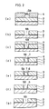
- Figs. 1 (a) to (k) show the state in which a large device isolation region is formed on a semiconductor substrate by a method for forming device isolation regions according to one embodiment of the present invention.
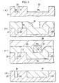
- Figs. 2 (a) to (k) correspond to Figs. 1 (a) to (k) and show the state in which a small device isolation region is formed on the same substrate according to common steps simultaneously with the formation of the large device isolation region.
- There will be described a method for forming semiconductor device isolation regions according to the present embodiment with reference to Figs. 1 (a) to (k) and 2 (a) to (k).
- Figs. 1 (k) and 2 (k) show the shape of sections of the large and small device isolation regions obtained in the series of steps mentioned above. As shown in Figs. 1 (k) and 2 (k), the widths of the device isolation regions finally obtained are equal to the widths Wa and Wb of the openings 5A and 5B of the resist patterns formed in the large and small isolation regions in the step (a), respectively.
- a large device isolation region can be formed more easily in a shorter time as designed, as compared with the conventional trench burying device isolation method.
- the device isolation region can be reduced to the limit of the lithography. Consequently, an integrated circuit will be made finer in future.
- the device isolation region is formed through the above-mentioned steps, a device such as a MOS transistor or capacitor is formed in an active region of the silicon substrate 1 according to a normal method.
- a semiconductor integrated circuit having the device isolation regions is perfected.
- the MOS transistor thus formed is measured. As a result, there can be obtained characteristics which are not inferior to those of a transistor isolated by the selective oxidation method and having the same size. In particular, there is no possibility that the defects of the silicon substrate are caused owing to increase in volume which appears in the case where the device isolation region is formed by only the selective oxidation method. Consequently, a backward leak characteristic value for junction is set to be extremely small. Referring to a parasitic MOS transistor which is necessarily formed between adjacent devices, even if an isolation width is 0.5 ⁇ m, a field inverted voltage and a field punch through voltage are not smaller than twice a supply voltage.
- the present invention relates to a method for forming semiconductor device isolation regions.
- Materials, means, numeric values and the like are not limited to those of the present embodiment except for Claims.
- an oxide film is formed in a central portion of the bottom of an opening with use of a second insulating film, which remains on the periphery of the bottom of the opening, as a mask.
- a trench is formed on the periphery of the bottom of the opening with use of the oxide film and a first insulating film as a mask.
- a device isolation region is formed by the oxide film and a third insulating film which buries the trench. Consequently, a lithography step is carried out only once in order to form the opening through all steps.
- the present invention can be applied from a very fine device isolation region to become the limit of lithography to a sufficiently large device isolation region. Furthermore, the device isolation regions having any size and shape can precisely be formed in accordance with a resist pattern formed in the lithography step. Accordingly, complicated conditions such as pattern shift and the like are eliminated so that a circuit layout can easily be made. In addition, the semiconductor integrated circuit can be made much finer.
- the oxidation time can be reduced. Furthermore, defects are not caused owing to increase in volume so that good device characteristics can be obtained.
Landscapes
- Element Separation (AREA)
- Local Oxidation Of Silicon (AREA)
Applications Claiming Priority (3)
| Application Number | Priority Date | Filing Date | Title |
|---|---|---|---|
| JP43394/90 | 1990-02-23 | ||
| JP4339490 | 1990-02-23 | ||
| JP2043394A JP2641781B2 (ja) | 1990-02-23 | 1990-02-23 | 半導体素子分離領域の形成方法 |
Publications (3)
| Publication Number | Publication Date |
|---|---|
| EP0443879A2 true EP0443879A2 (fr) | 1991-08-28 |
| EP0443879A3 EP0443879A3 (en) | 1993-03-10 |
| EP0443879B1 EP0443879B1 (fr) | 2000-04-19 |
Family
ID=12662574
Family Applications (1)
| Application Number | Title | Priority Date | Filing Date |
|---|---|---|---|
| EP91301459A Expired - Lifetime EP0443879B1 (fr) | 1990-02-23 | 1991-02-22 | Procédé pour la formation de régions d'isolation pour des dispositifs semi-conducteurs |
Country Status (5)
| Country | Link |
|---|---|
| US (1) | US5096848A (fr) |
| EP (1) | EP0443879B1 (fr) |
| JP (1) | JP2641781B2 (fr) |
| KR (1) | KR100195672B1 (fr) |
| DE (1) | DE69132117T2 (fr) |
Cited By (1)
| Publication number | Priority date | Publication date | Assignee | Title |
|---|---|---|---|---|
| EP0631307A3 (fr) * | 1993-06-14 | 1997-10-08 | Toshiba Kk | Dispositif semi-conducteur avec structure de rainure pour des régions d'isolation de composants et procédé de fabrication. |
Families Citing this family (75)
| Publication number | Priority date | Publication date | Assignee | Title |
|---|---|---|---|---|
| US5240512A (en) * | 1990-06-01 | 1993-08-31 | Texas Instruments Incorporated | Method and structure for forming a trench within a semiconductor layer of material |
| JP2608513B2 (ja) * | 1991-10-02 | 1997-05-07 | 三星電子株式会社 | 半導体装置の製造方法 |
| KR960008518B1 (en) * | 1991-10-02 | 1996-06-26 | Samsung Electronics Co Ltd | Manufacturing method and apparatus of semiconductor device |
| EP0635884A1 (fr) * | 1993-07-13 | 1995-01-25 | Siemens Aktiengesellschaft | Procédé pour la fabrication d'une rainure dans un substrat et application à la technologie de puissance vive |
| EP0641022B1 (fr) * | 1993-08-31 | 2006-05-17 | STMicroelectronics, Inc. | Structure d'isolation et procédé de sa fabrication |
| US5366925A (en) * | 1993-09-27 | 1994-11-22 | United Microelectronics Corporation | Local oxidation of silicon by using aluminum spiking technology |
| US5294562A (en) * | 1993-09-27 | 1994-03-15 | United Microelectronics Corporation | Trench isolation with global planarization using flood exposure |
| US5372968A (en) * | 1993-09-27 | 1994-12-13 | United Microelectronics Corporation | Planarized local oxidation by trench-around technology |
| US5308786A (en) * | 1993-09-27 | 1994-05-03 | United Microelectronics Corporation | Trench isolation for both large and small areas by means of silicon nodules after metal etching |
| KR960014452B1 (ko) * | 1993-12-22 | 1996-10-15 | 금성일렉트론 주식회사 | 반도체 소자분리 방법 |
| KR960014455B1 (ko) * | 1994-01-12 | 1996-10-15 | 금성일렉트론 주식회사 | 반도체장치의 및 그 제조방법 |
| US5371036A (en) * | 1994-05-11 | 1994-12-06 | United Microelectronics Corporation | Locos technology with narrow silicon trench |
| US5851887A (en) * | 1994-09-07 | 1998-12-22 | Cypress Semiconductor Corporation | Deep sub-micron polysilicon gap formation |
| JP2715972B2 (ja) * | 1995-03-04 | 1998-02-18 | 日本電気株式会社 | 半導体装置の製造方法 |
| KR100190010B1 (ko) * | 1995-12-30 | 1999-06-01 | 윤종용 | 반도체 소자의 소자분리막 형성방법 |
| US6124007A (en) | 1996-03-06 | 2000-09-26 | Scimed Life Systems Inc | Laminate catheter balloons with additive burst strength and methods for preparation of same |
| US5904539A (en) * | 1996-03-21 | 1999-05-18 | Advanced Micro Devices, Inc. | Semiconductor trench isolation process resulting in a silicon mesa having enhanced mechanical and electrical properties |
| WO1997038442A1 (fr) * | 1996-04-10 | 1997-10-16 | Advanced Micro Devices, Inc. | Isolement de tranchee de semi-conducteur associe a une methodologie amelioree de planarisation |
| US5926713A (en) * | 1996-04-17 | 1999-07-20 | Advanced Micro Devices, Inc. | Method for achieving global planarization by forming minimum mesas in large field areas |
| US5899727A (en) | 1996-05-02 | 1999-05-04 | Advanced Micro Devices, Inc. | Method of making a semiconductor isolation region bounded by a trench and covered with an oxide to improve planarization |
| KR980006053A (ko) * | 1996-06-26 | 1998-03-30 | 문정환 | 반도체장치의 격리막 형성방법 |
| US5944726A (en) * | 1996-08-23 | 1999-08-31 | Scimed Life Systems, Inc. | Stent delivery system having stent securement means |
| US6123712A (en) * | 1996-08-23 | 2000-09-26 | Scimed Life Systems, Inc. | Balloon catheter with stent securement means |
| US5980530A (en) | 1996-08-23 | 1999-11-09 | Scimed Life Systems Inc | Stent delivery system |
| US6077273A (en) | 1996-08-23 | 2000-06-20 | Scimed Life Systems, Inc. | Catheter support for stent delivery |
| US6391032B2 (en) | 1996-08-23 | 2002-05-21 | Scimed Life Systems, Inc. | Stent delivery system having stent securement means |
| CA2263492C (fr) * | 1996-08-23 | 2006-10-17 | Scimed Life Systems, Inc. | Systeme d'acheminement d'un stent, dote d'un appareil d'arrimage dudit stent |
| US6090685A (en) * | 1997-08-22 | 2000-07-18 | Micron Technology Inc. | Method of forming a LOCOS trench isolation structure |
| US6133610A (en) | 1998-01-20 | 2000-10-17 | International Business Machines Corporation | Silicon-on-insulator chip having an isolation barrier for reliability and process of manufacture |
| US6492684B2 (en) | 1998-01-20 | 2002-12-10 | International Business Machines Corporation | Silicon-on-insulator chip having an isolation barrier for reliability |
| TW396508B (en) * | 1999-01-05 | 2000-07-01 | Mosel Vitelic Inc | A method for forming trench isolation |
| US6727161B2 (en) | 2000-02-16 | 2004-04-27 | Cypress Semiconductor Corp. | Isolation technology for submicron semiconductor devices |
| US6726714B2 (en) * | 2001-08-09 | 2004-04-27 | Scimed Life Systems, Inc. | Stent delivery system |
| US6756284B2 (en) * | 2002-09-18 | 2004-06-29 | Silicon Storage Technology, Inc. | Method for forming a sublithographic opening in a semiconductor process |
| US6699772B1 (en) * | 2002-09-18 | 2004-03-02 | Gian Sharma | Hybrid trench isolation technology for high voltage isolation using thin field oxide in a semiconductor process |
| US7601285B2 (en) * | 2003-12-31 | 2009-10-13 | Boston Scientific Scimed, Inc. | Medical device with varying physical properties and method for forming same |
| US7264458B2 (en) * | 2004-01-07 | 2007-09-04 | Boston Scientific Scimed, Inc. | Process and apparatus for forming medical device balloons |
| US7016394B2 (en) * | 2004-04-23 | 2006-03-21 | Ucar Carbon Company Inc. | Male-female electrode joint |
| US7635510B2 (en) * | 2004-07-07 | 2009-12-22 | Boston Scientific Scimed, Inc. | High performance balloon catheter/component |
| US9586030B2 (en) * | 2004-12-23 | 2017-03-07 | Boston Scientific Scimed, Inc. | Fugitive plasticizer balloon surface treatment for enhanced stent securement |
| US20070009564A1 (en) * | 2005-06-22 | 2007-01-11 | Mcclain James B | Drug/polymer composite materials and methods of making the same |
| US20090062909A1 (en) | 2005-07-15 | 2009-03-05 | Micell Technologies, Inc. | Stent with polymer coating containing amorphous rapamycin |
| KR101406415B1 (ko) | 2005-07-15 | 2014-06-19 | 미셀 테크놀로지즈, 인코포레이티드 | 제어된 형태의 약물 분말을 함유하는 중합체 코팅 |
| US8043673B2 (en) | 2006-03-02 | 2011-10-25 | Boston Scientific Scimed, Inc. | Method to make tube-in-tube balloon |
| US8858855B2 (en) | 2006-04-20 | 2014-10-14 | Boston Scientific Scimed, Inc. | High pressure balloon |
| CA2996768C (fr) | 2006-04-26 | 2020-12-08 | Micell Technologies, Inc. | Revetements contenant plusieurs medicaments |
| US7943221B2 (en) * | 2006-05-22 | 2011-05-17 | Boston Scientific Scimed, Inc. | Hinged compliance fiber braid balloon |
| CA2667228C (fr) * | 2006-10-23 | 2015-07-14 | Micell Technologies, Inc. | Support pour charger electriquement un substrat au cours de l'enduction |
| US11426494B2 (en) | 2007-01-08 | 2022-08-30 | MT Acquisition Holdings LLC | Stents having biodegradable layers |
| CN101711137B (zh) | 2007-01-08 | 2014-10-22 | 米歇尔技术公司 | 具有可生物降解层的支架 |
| US9433516B2 (en) | 2007-04-17 | 2016-09-06 | Micell Technologies, Inc. | Stents having controlled elution |
| CN101854962B (zh) * | 2007-04-17 | 2015-12-16 | 米歇尔技术公司 | 具有生物降解性层的支架 |
| WO2008148013A1 (fr) | 2007-05-25 | 2008-12-04 | Micell Technologies, Inc. | Films de polymères pour le revêtement des dispositifs médicaux |
| US20100298928A1 (en) * | 2007-10-19 | 2010-11-25 | Micell Technologies, Inc. | Drug Coated Stents |
| JP5608160B2 (ja) | 2008-04-17 | 2014-10-15 | ミセル テクノロジーズ、インコーポレイテッド | 生体吸収性の層を有するステント |
| EP2313122B1 (fr) * | 2008-07-17 | 2019-03-06 | Micell Technologies, Inc. | Dispositif médical d administration de médicament |
| US8834913B2 (en) * | 2008-12-26 | 2014-09-16 | Battelle Memorial Institute | Medical implants and methods of making medical implants |
| WO2010111196A2 (fr) * | 2009-03-23 | 2010-09-30 | Micell Technologies, Inc. | Endoprothèses périphériques dotées de couches |
| JP2012522589A (ja) | 2009-04-01 | 2012-09-27 | ミシェル テクノロジーズ,インコーポレイテッド | 被覆ステント |
| EP2453834A4 (fr) | 2009-07-16 | 2014-04-16 | Micell Technologies Inc | Dispositif médical distributeur de médicament |
| EP2531140B1 (fr) * | 2010-02-02 | 2017-11-01 | Micell Technologies, Inc. | Endoprothèse et système de pose d'endoprothèse avec une capacité améliorée de pose |
| US8795762B2 (en) | 2010-03-26 | 2014-08-05 | Battelle Memorial Institute | System and method for enhanced electrostatic deposition and surface coatings |
| US10232092B2 (en) | 2010-04-22 | 2019-03-19 | Micell Technologies, Inc. | Stents and other devices having extracellular matrix coating |
| EP2593039B1 (fr) | 2010-07-16 | 2022-11-30 | Micell Technologies, Inc. | Dispositif médical d'administration de médicament |
| WO2012166819A1 (fr) | 2011-05-31 | 2012-12-06 | Micell Technologies, Inc. | Système et procédé de formation de revêtement transférable à élution de médicament, libéré dans le temps |
| CA2841360A1 (fr) | 2011-07-15 | 2013-01-24 | Micell Technologies, Inc. | Dispositif medical d'administration de medicament |
| US10188772B2 (en) | 2011-10-18 | 2019-01-29 | Micell Technologies, Inc. | Drug delivery medical device |
| EP2967803B1 (fr) | 2013-03-12 | 2023-12-27 | Micell Technologies, Inc. | Implants biomédicaux bioabsorbables |
| EP2996629B1 (fr) | 2013-05-15 | 2021-09-22 | Micell Technologies, Inc. | Implants biomedicaux bioabsorbables |
| EP3442642B1 (fr) | 2016-04-12 | 2025-10-15 | Boston Scientific Scimed, Inc. | Méthode de production d'un module de cathéter |
| WO2018111898A1 (fr) | 2016-12-13 | 2018-06-21 | Boston Scientific Scimed, Inc. | Ballonnet médical |
| WO2018200661A1 (fr) | 2017-04-25 | 2018-11-01 | Boston Scientific Scimed, Inc. | Ballonnet médical |
| US20200135898A1 (en) * | 2018-10-30 | 2020-04-30 | International Business Machines Corporation | Hard mask replenishment for etching processes |
| CN112086506B (zh) | 2020-10-20 | 2022-02-18 | 苏州东微半导体股份有限公司 | 半导体超结器件的制造方法 |
| CN112271134B (zh) * | 2020-10-20 | 2021-10-22 | 苏州东微半导体股份有限公司 | 半导体功率器件的制造方法 |
Family Cites Families (25)
| Publication number | Priority date | Publication date | Assignee | Title |
|---|---|---|---|---|
| JPS5146083A (en) * | 1974-10-18 | 1976-04-20 | Hitachi Ltd | Handotaisochino seizohoho |
| US4476623A (en) * | 1979-10-22 | 1984-10-16 | International Business Machines Corporation | Method of fabricating a bipolar dynamic memory cell |
| JPS5943545A (ja) * | 1982-09-06 | 1984-03-10 | Hitachi Ltd | 半導体集積回路装置 |
| JPS5958838A (ja) * | 1982-09-29 | 1984-04-04 | Hitachi Ltd | 半導体装置 |
| JPS6038832A (ja) * | 1983-08-12 | 1985-02-28 | Hitachi Ltd | 半導体装置とその製造方法 |
| US4569701A (en) * | 1984-04-05 | 1986-02-11 | At&T Bell Laboratories | Technique for doping from a polysilicon transfer layer |
| JPS60241231A (ja) * | 1984-05-15 | 1985-11-30 | Nippon Telegr & Teleph Corp <Ntt> | 半導体集積回路装置の製法 |
| USH204H (en) * | 1984-11-29 | 1987-02-03 | At&T Bell Laboratories | Method for implanting the sidewalls of isolation trenches |
| US4666557A (en) * | 1984-12-10 | 1987-05-19 | Ncr Corporation | Method for forming channel stops in vertical semiconductor surfaces |
| JP2589065B2 (ja) * | 1985-02-19 | 1997-03-12 | 三洋電機株式会社 | 半導体集積装置の製造方法 |
| US4641416A (en) * | 1985-03-04 | 1987-02-10 | Advanced Micro Devices, Inc. | Method of making an integrated circuit structure with self-aligned oxidation to isolate extrinsic base from emitter |
| US4653177A (en) * | 1985-07-25 | 1987-03-31 | At&T Bell Laboratories | Method of making and selectively doping isolation trenches utilized in CMOS devices |
| US4745081A (en) * | 1985-10-31 | 1988-05-17 | International Business Machines Corporation | Method of trench filling |
| US4892614A (en) * | 1986-07-07 | 1990-01-09 | Texas Instruments Incorporated | Integrated circuit isolation process |
| US4842675A (en) * | 1986-07-07 | 1989-06-27 | Texas Instruments Incorporated | Integrated circuit isolation process |
| JP2608054B2 (ja) * | 1986-10-20 | 1997-05-07 | 三菱電機株式会社 | 半導体記憶装置の製造方法 |
| JPS63114130A (ja) * | 1986-10-31 | 1988-05-19 | Hitachi Ltd | 素子間分離法 |
| JPS63122261A (ja) * | 1986-11-12 | 1988-05-26 | Mitsubishi Electric Corp | 半導体装置の製造方法 |
| JPS63188952A (ja) * | 1987-01-31 | 1988-08-04 | Toshiba Corp | 半導体装置の製造方法 |
| JPS63307756A (ja) * | 1987-06-09 | 1988-12-15 | Sony Corp | 半導体装置の製造方法 |
| US4861729A (en) * | 1987-08-24 | 1989-08-29 | Matsushita Electric Industrial Co., Ltd. | Method of doping impurities into sidewall of trench by use of plasma source |
| JPH01125971A (ja) * | 1987-11-11 | 1989-05-18 | Seiko Instr & Electron Ltd | C−mis型半導体装置とその製造方法 |
| DE3738643A1 (de) * | 1987-11-13 | 1989-05-24 | Siemens Ag | Verfahren zum herstellen von isolationsschichten in hochintegrierten halbleiterschaltungen |
| JPH01156897A (ja) * | 1987-12-15 | 1989-06-20 | Matsushita Electric Works Ltd | ワイヤレスセキュリティーシステム |
| JPH027529A (ja) * | 1988-06-27 | 1990-01-11 | Nec Corp | バイポーラトランジスタ及びその製造方法 |
-
1990
- 1990-02-23 JP JP2043394A patent/JP2641781B2/ja not_active Expired - Fee Related
-
1991
- 1991-02-11 US US07/653,074 patent/US5096848A/en not_active Expired - Fee Related
- 1991-02-21 KR KR1019910002803A patent/KR100195672B1/ko not_active Expired - Fee Related
- 1991-02-22 DE DE69132117T patent/DE69132117T2/de not_active Expired - Fee Related
- 1991-02-22 EP EP91301459A patent/EP0443879B1/fr not_active Expired - Lifetime
Cited By (1)
| Publication number | Priority date | Publication date | Assignee | Title |
|---|---|---|---|---|
| EP0631307A3 (fr) * | 1993-06-14 | 1997-10-08 | Toshiba Kk | Dispositif semi-conducteur avec structure de rainure pour des régions d'isolation de composants et procédé de fabrication. |
Also Published As
| Publication number | Publication date |
|---|---|
| DE69132117T2 (de) | 2000-09-28 |
| EP0443879A3 (en) | 1993-03-10 |
| JPH03245554A (ja) | 1991-11-01 |
| EP0443879B1 (fr) | 2000-04-19 |
| KR100195672B1 (ko) | 1999-06-15 |
| JP2641781B2 (ja) | 1997-08-20 |
| US5096848A (en) | 1992-03-17 |
| DE69132117D1 (de) | 2000-05-25 |
Similar Documents
| Publication | Publication Date | Title |
|---|---|---|
| US5096848A (en) | Method for forming semiconductor device isolating regions | |
| EP0476988B1 (fr) | Procédé pour la fabrication d'une région d'isolation d'un dispositif à semi-conducteur | |
| EP0444836B1 (fr) | Procédé pour former des régions d'isolation pour dispositifs semi-conducteurs | |
| US5308784A (en) | Semiconductor device and method for making the same | |
| US8330246B2 (en) | Intermediate structures for forming circuits | |
| US5258096A (en) | Method of forming local etch stop landing pads for simultaneous, self-aligned dry etching of contact vias with various depths | |
| US5706164A (en) | Method of fabricating high density integrated circuits, containing stacked capacitor DRAM devices, using elevated trench isolation and isolation spacers | |
| JP3640486B2 (ja) | メモリ・セルおよびメモリ・セル構造を製造する方法 | |
| JP3320794B2 (ja) | 波状素子接点コンデンサを形成するための方法 | |
| US6486558B2 (en) | Semiconductor device having a dummy pattern | |
| US6514819B1 (en) | High capacity stacked DRAM device and process for making a smaller geometry | |
| US8647949B2 (en) | Structure and method of fabricating a transistor having a trench gate | |
| KR100214917B1 (ko) | 반도체 장치 및 그 제조 방법 | |
| US5840591A (en) | Method of manufacturing buried bit line DRAM cell | |
| US20020197874A1 (en) | Self-aligned sti for narrow trenches | |
| US6667223B2 (en) | High aspect ratio high density plasma (HDP) oxide gapfill method in a lines and space pattern | |
| US5677232A (en) | Methods of fabricating combined field oxide/trench isolation regions | |
| EP0284456B1 (fr) | Procédé d'isolation comportant une interface protégée par une couche tampon de protection en oxyde | |
| EP0506473B1 (fr) | Procédé pour fabriquer des régions actives avec isolation planaire | |
| US6989307B2 (en) | Mask ROM, and fabrication method thereof | |
| JP3190144B2 (ja) | 半導体集積回路の製造方法 | |
| KR950002190B1 (ko) | 반도체장치의 소자분리방법 | |
| KR960003865B1 (ko) | 반도체 장치의 제조방법 | |
| KR0148611B1 (ko) | 반도체 소자의 소자분리막 형성방법 | |
| JP2003078000A (ja) | 半導体装置の製造方法 |
Legal Events
| Date | Code | Title | Description |
|---|---|---|---|
| PUAI | Public reference made under article 153(3) epc to a published international application that has entered the european phase |
Free format text: ORIGINAL CODE: 0009012 |
|
| 17P | Request for examination filed |
Effective date: 19910315 |
|
| AK | Designated contracting states |
Kind code of ref document: A2 Designated state(s): DE FR GB |
|
| PUAL | Search report despatched |
Free format text: ORIGINAL CODE: 0009013 |
|
| AK | Designated contracting states |
Kind code of ref document: A3 Designated state(s): DE FR GB |
|
| 17Q | First examination report despatched |
Effective date: 19930521 |
|
| GRAG | Despatch of communication of intention to grant |
Free format text: ORIGINAL CODE: EPIDOS AGRA |
|
| GRAG | Despatch of communication of intention to grant |
Free format text: ORIGINAL CODE: EPIDOS AGRA |
|
| GRAH | Despatch of communication of intention to grant a patent |
Free format text: ORIGINAL CODE: EPIDOS IGRA |
|
| GRAH | Despatch of communication of intention to grant a patent |
Free format text: ORIGINAL CODE: EPIDOS IGRA |
|
| GRAA | (expected) grant |
Free format text: ORIGINAL CODE: 0009210 |
|
| AK | Designated contracting states |
Kind code of ref document: B1 Designated state(s): DE FR GB |
|
| REF | Corresponds to: |
Ref document number: 69132117 Country of ref document: DE Date of ref document: 20000525 |
|
| ET | Fr: translation filed | ||
| PGFP | Annual fee paid to national office [announced via postgrant information from national office to epo] |
Ref country code: DE Payment date: 20010212 Year of fee payment: 11 |
|
| PGFP | Annual fee paid to national office [announced via postgrant information from national office to epo] |
Ref country code: FR Payment date: 20010213 Year of fee payment: 11 |
|
| PLBE | No opposition filed within time limit |
Free format text: ORIGINAL CODE: 0009261 |
|
| STAA | Information on the status of an ep patent application or granted ep patent |
Free format text: STATUS: NO OPPOSITION FILED WITHIN TIME LIMIT |
|
| PGFP | Annual fee paid to national office [announced via postgrant information from national office to epo] |
Ref country code: GB Payment date: 20010221 Year of fee payment: 11 |
|
| 26N | No opposition filed | ||
| REG | Reference to a national code |
Ref country code: GB Ref legal event code: IF02 |
|
| PG25 | Lapsed in a contracting state [announced via postgrant information from national office to epo] |
Ref country code: GB Free format text: LAPSE BECAUSE OF NON-PAYMENT OF DUE FEES Effective date: 20020222 |
|
| PG25 | Lapsed in a contracting state [announced via postgrant information from national office to epo] |
Ref country code: DE Free format text: LAPSE BECAUSE OF NON-PAYMENT OF DUE FEES Effective date: 20020903 |
|
| GBPC | Gb: european patent ceased through non-payment of renewal fee |
Effective date: 20020222 |
|
| PG25 | Lapsed in a contracting state [announced via postgrant information from national office to epo] |
Ref country code: FR Free format text: LAPSE BECAUSE OF NON-PAYMENT OF DUE FEES Effective date: 20021031 |
|
| REG | Reference to a national code |
Ref country code: FR Ref legal event code: ST |