EP0443920A1 - Verfahren zur gesteuerten Züchtung von nadelförmigen Kristallen und ihre Verwendung zur Herstellung spitzenförmiger Mikrokathoden - Google Patents
Verfahren zur gesteuerten Züchtung von nadelförmigen Kristallen und ihre Verwendung zur Herstellung spitzenförmiger Mikrokathoden Download PDFInfo
- Publication number
- EP0443920A1 EP0443920A1 EP91400395A EP91400395A EP0443920A1 EP 0443920 A1 EP0443920 A1 EP 0443920A1 EP 91400395 A EP91400395 A EP 91400395A EP 91400395 A EP91400395 A EP 91400395A EP 0443920 A1 EP0443920 A1 EP 0443920A1
- Authority
- EP
- European Patent Office
- Prior art keywords
- growth
- layer
- opening
- producing
- substrate
- Prior art date
- Legal status (The legal status is an assumption and is not a legal conclusion. Google has not performed a legal analysis and makes no representation as to the accuracy of the status listed.)
- Granted
Links
- 238000000034 method Methods 0.000 title claims abstract description 50
- 239000013078 crystal Substances 0.000 title claims description 22
- 239000000463 material Substances 0.000 claims abstract description 30
- 239000007788 liquid Substances 0.000 claims abstract description 21
- 239000000758 substrate Substances 0.000 claims abstract description 21
- 238000004519 manufacturing process Methods 0.000 claims abstract description 13
- 230000006911 nucleation Effects 0.000 claims abstract description 5
- 238000010899 nucleation Methods 0.000 claims abstract description 5
- 229910052710 silicon Inorganic materials 0.000 claims description 14
- 229910001218 Gallium arsenide Inorganic materials 0.000 claims description 12
- 238000000151 deposition Methods 0.000 claims description 11
- 229910052751 metal Inorganic materials 0.000 claims description 11
- 239000002184 metal Substances 0.000 claims description 11
- 238000001704 evaporation Methods 0.000 claims description 10
- 229910052733 gallium Inorganic materials 0.000 claims description 10
- 239000010703 silicon Substances 0.000 claims description 10
- 229910052785 arsenic Inorganic materials 0.000 claims description 9
- 230000008020 evaporation Effects 0.000 claims description 9
- 230000008021 deposition Effects 0.000 claims description 8
- 239000012071 phase Substances 0.000 claims description 8
- GYHNNYVSQQEPJS-UHFFFAOYSA-N Gallium Chemical compound [Ga] GYHNNYVSQQEPJS-UHFFFAOYSA-N 0.000 claims description 7
- RBFQJDQYXXHULB-UHFFFAOYSA-N arsane Chemical compound [AsH3] RBFQJDQYXXHULB-UHFFFAOYSA-N 0.000 claims description 7
- RQNWIZPPADIBDY-UHFFFAOYSA-N arsenic atom Chemical compound [As] RQNWIZPPADIBDY-UHFFFAOYSA-N 0.000 claims description 7
- 229910000070 arsenic hydride Inorganic materials 0.000 claims description 7
- 239000000470 constituent Substances 0.000 claims description 7
- BLRPTPMANUNPDV-UHFFFAOYSA-N Silane Chemical compound [SiH4] BLRPTPMANUNPDV-UHFFFAOYSA-N 0.000 claims description 5
- 229910052737 gold Inorganic materials 0.000 claims description 5
- XOYLJNJLGBYDTH-UHFFFAOYSA-M chlorogallium Chemical compound [Ga]Cl XOYLJNJLGBYDTH-UHFFFAOYSA-M 0.000 claims description 4
- 239000012808 vapor phase Substances 0.000 claims description 4
- 229910003910 SiCl4 Inorganic materials 0.000 claims description 2
- 229910003818 SiH2Cl2 Inorganic materials 0.000 claims description 2
- 239000004020 conductor Substances 0.000 claims description 2
- 229910052802 copper Inorganic materials 0.000 claims description 2
- 239000003989 dielectric material Substances 0.000 claims description 2
- 238000010438 heat treatment Methods 0.000 claims description 2
- 229910052763 palladium Inorganic materials 0.000 claims description 2
- 229910052697 platinum Inorganic materials 0.000 claims description 2
- FDNAPBUWERUEDA-UHFFFAOYSA-N silicon tetrachloride Chemical compound Cl[Si](Cl)(Cl)Cl FDNAPBUWERUEDA-UHFFFAOYSA-N 0.000 claims description 2
- 229910000041 hydrogen chloride Inorganic materials 0.000 claims 1
- 229910052749 magnesium Inorganic materials 0.000 claims 1
- VYPSYNLAJGMNEJ-UHFFFAOYSA-N Silicium dioxide Chemical compound O=[Si]=O VYPSYNLAJGMNEJ-UHFFFAOYSA-N 0.000 description 28
- 239000000377 silicon dioxide Substances 0.000 description 14
- 229910052681 coesite Inorganic materials 0.000 description 11
- 229910052906 cristobalite Inorganic materials 0.000 description 11
- 239000007789 gas Substances 0.000 description 11
- 235000012239 silicon dioxide Nutrition 0.000 description 11
- 229910052682 stishovite Inorganic materials 0.000 description 11
- 229910052905 tridymite Inorganic materials 0.000 description 11
- XUIMIQQOPSSXEZ-UHFFFAOYSA-N Silicon Chemical compound [Si] XUIMIQQOPSSXEZ-UHFFFAOYSA-N 0.000 description 10
- 239000011347 resin Substances 0.000 description 8
- 229920005989 resin Polymers 0.000 description 8
- 235000015041 whisky Nutrition 0.000 description 8
- 239000007787 solid Substances 0.000 description 7
- 229910045601 alloy Inorganic materials 0.000 description 6
- 239000000956 alloy Substances 0.000 description 6
- 230000007423 decrease Effects 0.000 description 5
- 239000010931 gold Substances 0.000 description 5
- 238000005275 alloying Methods 0.000 description 4
- PCHJSUWPFVWCPO-UHFFFAOYSA-N gold Chemical compound [Au] PCHJSUWPFVWCPO-UHFFFAOYSA-N 0.000 description 4
- 239000011159 matrix material Substances 0.000 description 4
- 230000003647 oxidation Effects 0.000 description 4
- 238000007254 oxidation reaction Methods 0.000 description 4
- 229910052581 Si3N4 Inorganic materials 0.000 description 3
- 230000015572 biosynthetic process Effects 0.000 description 3
- 239000000203 mixture Substances 0.000 description 3
- 238000001020 plasma etching Methods 0.000 description 3
- 238000001179 sorption measurement Methods 0.000 description 3
- RGGPNXQUMRMPRA-UHFFFAOYSA-N triethylgallium Chemical compound CC[Ga](CC)CC RGGPNXQUMRMPRA-UHFFFAOYSA-N 0.000 description 3
- XCZXGTMEAKBVPV-UHFFFAOYSA-N trimethylgallium Chemical compound C[Ga](C)C XCZXGTMEAKBVPV-UHFFFAOYSA-N 0.000 description 3
- PEDCQBHIVMGVHV-UHFFFAOYSA-N Glycerine Chemical compound OCC(O)CO PEDCQBHIVMGVHV-UHFFFAOYSA-N 0.000 description 2
- 239000002156 adsorbate Substances 0.000 description 2
- 229910052782 aluminium Inorganic materials 0.000 description 2
- 238000003491 array Methods 0.000 description 2
- OEYOHULQRFXULB-UHFFFAOYSA-N arsenic trichloride Chemical compound Cl[As](Cl)Cl OEYOHULQRFXULB-UHFFFAOYSA-N 0.000 description 2
- 239000002131 composite material Substances 0.000 description 2
- 230000003247 decreasing effect Effects 0.000 description 2
- 238000004090 dissolution Methods 0.000 description 2
- 238000005516 engineering process Methods 0.000 description 2
- 230000005669 field effect Effects 0.000 description 2
- 238000010348 incorporation Methods 0.000 description 2
- 239000007791 liquid phase Substances 0.000 description 2
- 230000004807 localization Effects 0.000 description 2
- 238000002161 passivation Methods 0.000 description 2
- 239000004065 semiconductor Substances 0.000 description 2
- 238000007493 shaping process Methods 0.000 description 2
- 229910015371 AuCu Inorganic materials 0.000 description 1
- 241000252203 Clupea harengus Species 0.000 description 1
- XYFCBTPGUUZFHI-UHFFFAOYSA-N Phosphine Chemical compound P XYFCBTPGUUZFHI-UHFFFAOYSA-N 0.000 description 1
- 229910000676 Si alloy Inorganic materials 0.000 description 1
- 229910003822 SiHCl3 Inorganic materials 0.000 description 1
- 229910052787 antimony Inorganic materials 0.000 description 1
- 229910002056 binary alloy Inorganic materials 0.000 description 1
- 239000012159 carrier gas Substances 0.000 description 1
- FFCZHQLUEDCQKI-UHFFFAOYSA-N diarsenic Chemical compound [As]#[As] FFCZHQLUEDCQKI-UHFFFAOYSA-N 0.000 description 1
- ZOCHARZZJNPSEU-UHFFFAOYSA-N diboron Chemical compound B#B ZOCHARZZJNPSEU-UHFFFAOYSA-N 0.000 description 1
- 230000000694 effects Effects 0.000 description 1
- 230000005611 electricity Effects 0.000 description 1
- 238000010894 electron beam technology Methods 0.000 description 1
- 239000008246 gaseous mixture Substances 0.000 description 1
- 235000019514 herring Nutrition 0.000 description 1
- 239000012535 impurity Substances 0.000 description 1
- 238000001465 metallisation Methods 0.000 description 1
- 229910021420 polycrystalline silicon Inorganic materials 0.000 description 1
- 239000002243 precursor Substances 0.000 description 1
- 230000000750 progressive effect Effects 0.000 description 1
- 229910052709 silver Inorganic materials 0.000 description 1
- 238000001947 vapour-phase growth Methods 0.000 description 1
Images


Classifications
-
- H—ELECTRICITY
- H01—ELECTRIC ELEMENTS
- H01J—ELECTRIC DISCHARGE TUBES OR DISCHARGE LAMPS
- H01J9/00—Apparatus or processes specially adapted for the manufacture, installation, removal, maintenance of electric discharge tubes, discharge lamps, or parts thereof; Recovery of material from discharge tubes or lamps
- H01J9/02—Manufacture of electrodes or electrode systems
- H01J9/022—Manufacture of electrodes or electrode systems of cold cathodes
- H01J9/025—Manufacture of electrodes or electrode systems of cold cathodes of field emission cathodes
-
- C—CHEMISTRY; METALLURGY
- C30—CRYSTAL GROWTH
- C30B—SINGLE-CRYSTAL GROWTH; UNIDIRECTIONAL SOLIDIFICATION OF EUTECTIC MATERIAL OR UNIDIRECTIONAL DEMIXING OF EUTECTOID MATERIAL; REFINING BY ZONE-MELTING OF MATERIAL; PRODUCTION OF A HOMOGENEOUS POLYCRYSTALLINE MATERIAL WITH DEFINED STRUCTURE; SINGLE CRYSTALS OR HOMOGENEOUS POLYCRYSTALLINE MATERIAL WITH DEFINED STRUCTURE; AFTER-TREATMENT OF SINGLE CRYSTALS OR A HOMOGENEOUS POLYCRYSTALLINE MATERIAL WITH DEFINED STRUCTURE; APPARATUS THEREFOR
- C30B11/00—Single-crystal growth by normal freezing or freezing under temperature gradient, e.g. Bridgman-Stockbarger method
- C30B11/04—Single-crystal growth by normal freezing or freezing under temperature gradient, e.g. Bridgman-Stockbarger method adding crystallising materials or reactants forming it in situ to the melt
- C30B11/08—Single-crystal growth by normal freezing or freezing under temperature gradient, e.g. Bridgman-Stockbarger method adding crystallising materials or reactants forming it in situ to the melt every component of the crystal composition being added during the crystallisation
- C30B11/12—Vaporous components, e.g. vapour-liquid-solid-growth
-
- C—CHEMISTRY; METALLURGY
- C30—CRYSTAL GROWTH
- C30B—SINGLE-CRYSTAL GROWTH; UNIDIRECTIONAL SOLIDIFICATION OF EUTECTIC MATERIAL OR UNIDIRECTIONAL DEMIXING OF EUTECTOID MATERIAL; REFINING BY ZONE-MELTING OF MATERIAL; PRODUCTION OF A HOMOGENEOUS POLYCRYSTALLINE MATERIAL WITH DEFINED STRUCTURE; SINGLE CRYSTALS OR HOMOGENEOUS POLYCRYSTALLINE MATERIAL WITH DEFINED STRUCTURE; AFTER-TREATMENT OF SINGLE CRYSTALS OR A HOMOGENEOUS POLYCRYSTALLINE MATERIAL WITH DEFINED STRUCTURE; APPARATUS THEREFOR
- C30B23/00—Single-crystal growth by condensing evaporated or sublimed materials
- C30B23/007—Growth of whiskers or needles
-
- C—CHEMISTRY; METALLURGY
- C30—CRYSTAL GROWTH
- C30B—SINGLE-CRYSTAL GROWTH; UNIDIRECTIONAL SOLIDIFICATION OF EUTECTIC MATERIAL OR UNIDIRECTIONAL DEMIXING OF EUTECTOID MATERIAL; REFINING BY ZONE-MELTING OF MATERIAL; PRODUCTION OF A HOMOGENEOUS POLYCRYSTALLINE MATERIAL WITH DEFINED STRUCTURE; SINGLE CRYSTALS OR HOMOGENEOUS POLYCRYSTALLINE MATERIAL WITH DEFINED STRUCTURE; AFTER-TREATMENT OF SINGLE CRYSTALS OR A HOMOGENEOUS POLYCRYSTALLINE MATERIAL WITH DEFINED STRUCTURE; APPARATUS THEREFOR
- C30B25/00—Single-crystal growth by chemical reaction of reactive gases, e.g. chemical vapour-deposition growth
- C30B25/005—Growth of whiskers or needles
-
- C—CHEMISTRY; METALLURGY
- C30—CRYSTAL GROWTH
- C30B—SINGLE-CRYSTAL GROWTH; UNIDIRECTIONAL SOLIDIFICATION OF EUTECTIC MATERIAL OR UNIDIRECTIONAL DEMIXING OF EUTECTOID MATERIAL; REFINING BY ZONE-MELTING OF MATERIAL; PRODUCTION OF A HOMOGENEOUS POLYCRYSTALLINE MATERIAL WITH DEFINED STRUCTURE; SINGLE CRYSTALS OR HOMOGENEOUS POLYCRYSTALLINE MATERIAL WITH DEFINED STRUCTURE; AFTER-TREATMENT OF SINGLE CRYSTALS OR A HOMOGENEOUS POLYCRYSTALLINE MATERIAL WITH DEFINED STRUCTURE; APPARATUS THEREFOR
- C30B29/00—Single crystals or homogeneous polycrystalline material with defined structure characterised by the material or by their shape
- C30B29/02—Elements
- C30B29/06—Silicon
Definitions
- the invention relates to a process for the controlled growth of needle crystals and its application to the production of pointed microcathodes. More particularly, the invention relates to the field of controlled growth of filamentary single crystals of the ⁇ whiskers ⁇ type. It allows, by means of a known method (VLS method) developed in the sixties to obtain regular matrices of filamentary crystals of controlled height and diameter.
- VLS method known method developed in the sixties to obtain regular matrices of filamentary crystals of controlled height and diameter.
- Whiskers are filamentary monocrocrystals with a length to diameter ratio greater than 10. They have been known for a very long time, but interest in this type of crystal was stimulated in the early 1950s when Herring and Galt, in the document Physical Review 85, (1952), 1060, demonstrated that these crystals had mechanical properties similar to those of single crystals.
- the dissolved adsorbate causes a supersaturation of the liquid which then expels the solid at the liquid / solid interface, so as to return to equilibrium; the drop of liquid rises gradually on the expelled crystal which takes the form of a whisker with a diameter equal to that of the drop of liquid.
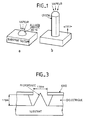
- Figures 1a and 1b show the VLS principle applied to silicon, but it is obvious that one can use a variety of different substrates associated with drops of liquid also very varied. (See for example GIVARGIZOV already cited).
- the present invention relates to a process for controlled growth of filamentary single crystals (whiskers) using the VLS method.
- the invention therefore makes it possible to produce filamentary single crystals at selected points on the surface of the substrate and to produce, for example, matrices of filaments.
- the invention also relates to a method for producing a microcathode with spikes applying the above method, characterized in that it comprises, before the second production stage, a phase of production of a third layer of a conductive material of the electricity followed by another phase of producing a fourth layer of dielectric material.
- a substrate of Si for example or of GaAs preferably of orientation (111) on which a layer 1 of SiO2 of thickness typically between 0.1 micrometers and a few micrometers is deposited (or obtained by oxidation).
- a layer of photosensitive resin (or a metallic surface mask) is then deposited which is exposed and developed (optically or with the aid of an electron beam) so as to produce substantially circular openings 5 with a diameter between 0, 1 and 2 ⁇ m in steps of 0.5 to a few microns.
- a layer of metal such as gold (or Ag, Cu, Pt, Pd, Ni, Gd, Mg, Os, ...) with a thickness of 1 nm at 500 nm, which will be adapted to the diameter of the openings in SiO2 (the smaller the diameter of the openings, the smaller the thickness of the metal layer).
- the resin or the metal mask is then dissolved (FIG. 2e) (in the latter case an electrochemical dissolution is carried out) so as to eliminate the resin and the deposit of Au located on the aforementioned resin.
- metallic points for example of gold
- the substrate thus obtained is introduced into a CVD deposition reactor in an SiH4 + HCl or SiH2Cl2 + HCl or SiCl4 atmosphere, or else SiHCl3 + HCl (still using as carrier gas H2) and wear the temperature between typically 400 and 1000 ° C.
- the metal deposits have been produced in the form of a matrix, it is possible to obtain a matrix of filamentary single crystals (whiskers).
- the grid is passivated using a very thin layer of SiO2 or Si3N4 3, so as to avoid nucleation on the latter during the subsequent deposition operation; a layer 4 of resin is deposited on the assembly.
- openings such as 5 in the composite structure previously obtained. These openings are typically circular and have a diameter of between 0.1 and 2 micrometers, for example.
- the pitch of these openings can be from 0.5 micrometers to a few micrometers.
- Whiskers such as 6 are then grown (FIG. 4e) from the molten metallized zones (such as zone 5) in the same manner as that described above.
- the temperature is varied during the deposition step, it is possible to obtain a variation in the diameter of the whiskeys.
- the decrease in temperature causes a decrease in this diameter.
- Me-Si alloys where Me is a very sparingly soluble metal (solubility of the order of 1015 to 1017 at / cm3 in silicon or in GaAs and in general in the material of the substrate).
- One can however use an alloy for example Sb - Si, As - Si, Ga - Si, Al - Si ! in which the metal or the semi-metal (Al, Ga, As, Sb ”) in the growth zones of the whiskeys and constituting the alloy is very soluble in silicon (or in GaAs or in the substrate) with a solubility typically greater than 1019 at / cm3.
- the maximum solubility at 1000 ° C in Si is 1.8 1021 / cm3.
- GaAs substrate Another example concerns the use of a GaAs substrate.
- one will have, in the micrologations, of gallium and one will operate under flow of AsH3 or As2 or As4.
- AsH3 or As2 or As4 As a result, a growth of GaAs will be obtained which will stop by itself when the gallium of the drop has been incorporated into the crystal.
- Figure 5 summarizes this principle by showing at different times ti (ti + 1> ti) the morphology of the droplet and the underlying crystal. As time increases, the size of the droplet decreases, which leads to shaping of the microtip. Different geometric parameters are specified for information in Figure 5.
- Another method for forming localized microdrops can also be put into practice using a starting substrate of Ga As on which a layer 16 of SiO2 or Si3N4 (thickness 6a) is first of all deposited between 0, 1 and 10 ⁇ m typically.
- Micrologations 5 (FIG. 6b) are etched into this dielectric layer as in the previous process.
- the Ga As substrate is then heated in a controlled manner (in a sealed evacuated or swept enclosure), which has the effect of evaporating arsenic and therefore of revealing droplets of Ga located at the place where it takes place. preferential evaporation, that is to say in micrologations 5. There is therefore a self-alignment of the droplets with the dielectric housings (FIG. 6c).
- a gaseous growth mixture of GaCl + As4 type obtained for example, is introduced into a VPE reactor by the arsenic trichloride method (AsCl3) or else a mixture such as AsH3 + TMG (trimethyl gallium) or TEG (triethyl gallium) so as to obtain the growth of GaAs whiskers (FIG. 6d).
- AsCl3 arsenic trichloride method
- TMG trimethyl gallium
- TEG triethyl gallium
- Figures 7a to 7d show a variant of this process.
- a layer 7 of GaAs is deposited on a silicon substrate.
- Layer 7 is then covered with a layer 16 of SiO2 or Si3N4 ( Figure 7a).
- openings 5 are made in layer 16 (FIG. 7b).
- the substrate could be another semiconductor material than silicon.
- a layer 7 of a material is produced, which by evaporation, provides in each opening 5, a liquid constituent capable of absorbing the or the constituents (in the form of gaseous precursors) of the material to be grown in the form of whiskers.
- the shape of the microtips can be shaped by other techniques.
- an element of the alloy of the drop of liquid may be slightly volatile when heated. For example, if arsenic is present in this alloy, this arsenic will be stabilized by adding AsH3 to the gas flow during growth.
- a corrosive gas making it possible to attack at least one of the elements of the liquid alloy.
- a corrosive gas making it possible to attack at least one of the elements of the liquid alloy.
Landscapes
- Chemical & Material Sciences (AREA)
- Engineering & Computer Science (AREA)
- Crystallography & Structural Chemistry (AREA)
- Materials Engineering (AREA)
- Metallurgy (AREA)
- Organic Chemistry (AREA)
- Chemical Kinetics & Catalysis (AREA)
- General Chemical & Material Sciences (AREA)
- Manufacturing & Machinery (AREA)
- Cold Cathode And The Manufacture (AREA)
- Crystals, And After-Treatments Of Crystals (AREA)
Applications Claiming Priority (2)
| Application Number | Priority Date | Filing Date | Title |
|---|---|---|---|
| FR9002258A FR2658839B1 (fr) | 1990-02-23 | 1990-02-23 | Procede de croissance controlee de cristaux aciculaires et application a la realisation de microcathodes a pointes. |
| FR9002258 | 1990-02-23 |
Publications (2)
| Publication Number | Publication Date |
|---|---|
| EP0443920A1 true EP0443920A1 (de) | 1991-08-28 |
| EP0443920B1 EP0443920B1 (de) | 1994-11-02 |
Family
ID=9394066
Family Applications (1)
| Application Number | Title | Priority Date | Filing Date |
|---|---|---|---|
| EP91400395A Expired - Lifetime EP0443920B1 (de) | 1990-02-23 | 1991-02-15 | Verfahren zur gesteuerten Züchtung von nadelförmigen Kristallen und ihre Verwendung zur Herstellung spitzenförmiger Mikrokathoden |
Country Status (5)
| Country | Link |
|---|---|
| US (1) | US5314569A (de) |
| EP (1) | EP0443920B1 (de) |
| JP (1) | JPH0597598A (de) |
| DE (1) | DE69104864T2 (de) |
| FR (1) | FR2658839B1 (de) |
Cited By (19)
| Publication number | Priority date | Publication date | Assignee | Title |
|---|---|---|---|---|
| WO1993005530A1 (en) * | 1991-09-02 | 1993-03-18 | Era Patents Ltd. | Production of fine points on a substrate |
| FR2719155A1 (fr) * | 1994-04-25 | 1995-10-27 | Commissariat Energie Atomique | Procédé de réalisation de sources d'électrons à micropointes et source d'électrons à micropointes obtenue par ce procédé. |
| FR2719156A1 (fr) * | 1994-04-25 | 1995-10-27 | Commissariat Energie Atomique | Source d'électrons à micropointes, les micropointes comportant deux parties. |
| WO1997037064A1 (en) * | 1996-04-01 | 1997-10-09 | Evgeny Invievich Givargizov | Method and apparatus for growing oriented whisker arrays |
| EP0738791A4 (de) * | 1994-11-10 | 1998-04-01 | Josuke Nakata | Verfahren zur herstellung sphärischer kristalle |
| EP0838865A3 (de) * | 1996-10-28 | 2000-10-18 | Sony Corporation | Auf einem Substrat hergestellte Quantendrähte und deren Herstellungsverfahren, sowie ein Bauteil mit Quantendrähten auf einem Substrat |
| US7335908B2 (en) | 2002-07-08 | 2008-02-26 | Qunano Ab | Nanostructures and methods for manufacturing the same |
| US7354850B2 (en) | 2004-02-06 | 2008-04-08 | Qunano Ab | Directionally controlled growth of nanowhiskers |
| US7432522B2 (en) | 2003-04-04 | 2008-10-07 | Qunano Ab | Nanowhiskers with pn junctions, doped nanowhiskers, and methods for preparing them |
| US7528002B2 (en) | 2004-06-25 | 2009-05-05 | Qunano Ab | Formation of nanowhiskers on a substrate of dissimilar material |
| US7826336B2 (en) | 2006-02-23 | 2010-11-02 | Qunano Ab | Data storage nanostructures |
| US8049203B2 (en) | 2006-12-22 | 2011-11-01 | Qunano Ab | Nanoelectronic structure and method of producing such |
| GB2482915A (en) * | 2010-08-20 | 2012-02-22 | Univ Montfort | Growing Silicon by Plasma Enhanced Chemical Vapour Deposition |
| US8183587B2 (en) | 2006-12-22 | 2012-05-22 | Qunano Ab | LED with upstanding nanowire structure and method of producing such |
| US8227817B2 (en) | 2006-12-22 | 2012-07-24 | Qunano Ab | Elevated LED |
| US8685877B2 (en) | 2006-12-22 | 2014-04-01 | Imec | Doping of nanostructures |
| US8790462B2 (en) | 2003-04-04 | 2014-07-29 | Qunano Ab | Precisely positioned nanowhiskers and nanowhisker arrays and method for preparing them |
| US10263149B2 (en) | 2006-12-22 | 2019-04-16 | Qunano Ab | Nanostructured LED array with collimating reflectors |
| RU2750732C1 (ru) * | 2020-06-29 | 2021-07-01 | Федеральное государственное бюджетное образования учреждение высшего образования "Воронежский государственный технический университет" | Способ выращивания нитевидных кристаллов кремния |
Families Citing this family (41)
| Publication number | Priority date | Publication date | Assignee | Title |
|---|---|---|---|---|
| JP2821061B2 (ja) * | 1992-05-22 | 1998-11-05 | 電気化学工業株式会社 | 単結晶の製造方法 |
| US6614161B1 (en) * | 1993-07-20 | 2003-09-02 | University Of Georgia Research Foundation, Inc. | Resonant microcavity display |
| RU2074444C1 (ru) * | 1994-07-26 | 1997-02-27 | Евгений Инвиевич Гиваргизов | Матричный автоэлектронный катод и электронный прибор для оптического отображения информации |
| US5431127A (en) * | 1994-10-14 | 1995-07-11 | Texas Instruments Incorporated | Process for producing semiconductor spheres |
| AU5733896A (en) * | 1995-06-05 | 1996-12-24 | Evan L. Ragland | Triode apparatus for control of nuclear fusion |
| JP3099754B2 (ja) * | 1996-10-23 | 2000-10-16 | 日本電気株式会社 | プローブカードの製造方法 |
| FR2780808B1 (fr) | 1998-07-03 | 2001-08-10 | Thomson Csf | Dispositif a emission de champ et procedes de fabrication |
| RU2139373C1 (ru) * | 1998-07-07 | 1999-10-10 | Макин Владимир Сергеевич | Способ формирования выступа типа острия |
| JP4615657B2 (ja) * | 2000-01-26 | 2011-01-19 | 雅介 高田 | 酸化亜鉛単結晶およびその製造方法 |
| FR2832995B1 (fr) * | 2001-12-04 | 2004-02-27 | Thales Sa | Procede de croissance catalytique de nanotubes ou nanofibres comprenant une barriere de diffusion de type alliage nisi |
| KR20030059936A (ko) * | 2002-01-03 | 2003-07-12 | 강윤묵 | 실리콘 나노 결정을 형성하는 새로운 공정. |
| JP4140765B2 (ja) | 2002-09-19 | 2008-08-27 | コバレントマテリアル株式会社 | 針状シリコン結晶およびその製造方法 |
| US6605535B1 (en) * | 2002-09-26 | 2003-08-12 | Promos Technologies, Inc | Method of filling trenches using vapor-liquid-solid mechanism |
| FR2860780B1 (fr) | 2003-10-13 | 2006-05-19 | Centre Nat Rech Scient | Procede de synthese de structures filamentaires nanometriques et composants pour l'electronique comprenant de telles structures |
| US20050112048A1 (en) * | 2003-11-25 | 2005-05-26 | Loucas Tsakalakos | Elongated nano-structures and related devices |
| FR2870037B1 (fr) * | 2004-05-04 | 2006-07-14 | Commissariat Energie Atomique | Systeme d'enregistrement d'informations et procede d'utilisation d'un tel systeme |
| JP4607513B2 (ja) * | 2004-07-27 | 2011-01-05 | 株式会社アルバック | カソード基板及びこのカソード基板の作製方法。 |
| FR2879342B1 (fr) * | 2004-12-15 | 2008-09-26 | Thales Sa | Cathode a emission de champ, a commande optique |
| US7385231B2 (en) | 2005-08-31 | 2008-06-10 | Fujifilmcorporation | Porous thin-film-deposition substrate, electron emitting element, methods of producing them, and switching element and display element |
| US7951422B2 (en) * | 2005-12-29 | 2011-05-31 | Nanosys, Inc. | Methods for oriented growth of nanowires on patterned substrates |
| JP5137095B2 (ja) * | 2006-02-20 | 2013-02-06 | 国立大学法人 筑波大学 | シリコンナノ結晶材料の製造方法及び該製造方法で製造されたシリコンナノ結晶材料 |
| US20080191317A1 (en) * | 2007-02-13 | 2008-08-14 | International Business Machines Corporation | Self-aligned epitaxial growth of semiconductor nanowires |
| CN101779271B (zh) * | 2007-07-19 | 2013-05-22 | 加利福尼亚技术学院 | 垂直排列的硅线阵列的结构及其形成方法 |
| KR20100044854A (ko) * | 2007-07-19 | 2010-04-30 | 캘리포니아 인스티튜트 오브 테크놀로지 | 반도체의 정렬된 어레이의 구조 |
| US7781853B2 (en) * | 2007-07-26 | 2010-08-24 | Hewlett-Packard Development Company, L.P. | Plasmon-enhanced electromagnetic-radiation-emitting devices and methods for fabricating the same |
| JP2010538464A (ja) * | 2007-08-28 | 2010-12-09 | カリフォルニア インスティテュート オブ テクノロジー | ポリマ埋め込み型半導体ロッドアレイ |
| US8084337B2 (en) * | 2007-10-26 | 2011-12-27 | Qunano Ab | Growth of III-V compound semiconductor nanowires on silicon substrates |
| US7927905B2 (en) * | 2007-12-21 | 2011-04-19 | Palo Alto Research Center Incorporated | Method of producing microsprings having nanowire tip structures |
| US8247033B2 (en) | 2008-09-19 | 2012-08-21 | The University Of Massachusetts | Self-assembly of block copolymers on topographically patterned polymeric substrates |
| US8518837B2 (en) | 2008-09-25 | 2013-08-27 | The University Of Massachusetts | Method of producing nanopatterned articles using surface-reconstructed block copolymer films |
| WO2011066570A2 (en) * | 2009-11-30 | 2011-06-03 | California Institute Of Technology | Semiconductor wire array structures, and solar cells and photodetectors based on such structures |
| WO2011156042A2 (en) | 2010-03-23 | 2011-12-15 | California Institute Of Technology | Heterojunction wire array solar cells |
| US9156682B2 (en) | 2011-05-25 | 2015-10-13 | The University Of Massachusetts | Method of forming oriented block copolymer line patterns, block copolymer line patterns formed thereby, and their use to form patterned articles |
| US9476129B2 (en) | 2012-04-02 | 2016-10-25 | California Institute Of Technology | Solar fuels generator |
| US10026560B2 (en) | 2012-01-13 | 2018-07-17 | The California Institute Of Technology | Solar fuels generator |
| WO2013106793A1 (en) | 2012-01-13 | 2013-07-18 | California Institute Of Technology | Solar fuel generators |
| WO2013126432A1 (en) | 2012-02-21 | 2013-08-29 | California Institute Of Technology | Axially-integrated epitaxially-grown tandem wire arrays |
| CN102623393B (zh) * | 2012-03-15 | 2014-06-04 | 华中科技大学 | 一种利用锡须生长填充微孔的方法 |
| US9947816B2 (en) | 2012-04-03 | 2018-04-17 | California Institute Of Technology | Semiconductor structures for fuel generation |
| US9553223B2 (en) | 2013-01-24 | 2017-01-24 | California Institute Of Technology | Method for alignment of microwires |
| KR20220152325A (ko) * | 2020-03-24 | 2022-11-15 | 에펜코 오우 | 플라즈마 연소를 안정화하고 보조하기 위한 나노크기의 세라믹 플라즈마 촉매 |
Citations (3)
| Publication number | Priority date | Publication date | Assignee | Title |
|---|---|---|---|---|
| US3493431A (en) * | 1966-11-25 | 1970-02-03 | Bell Telephone Labor Inc | Vapor-liquid-solid crystal growth technique |
| EP0278405A2 (de) * | 1987-02-06 | 1988-08-17 | Canon Kabushiki Kaisha | Elektronen emittierendes Element und dessen Herstellungsverfahren |
| WO1989009479A1 (fr) * | 1988-03-25 | 1989-10-05 | Thomson-Csf | Procede de fabrication de sources d'electrons du type a emission de champ, et son application a la realisation de reseaux d'emetteurs |
Family Cites Families (6)
| Publication number | Priority date | Publication date | Assignee | Title |
|---|---|---|---|---|
| NL143436B (nl) * | 1966-12-14 | 1974-10-15 | Philips Nv | Werkwijze voor het vervaardigen van draadvormige siliciumcarbide kristallen en voorwerpen geheel of voor een deel bestaande uit deze kristallen. |
| US3580732A (en) * | 1968-01-15 | 1971-05-25 | Ibm | Method of growing single crystals |
| US3549432A (en) * | 1968-07-15 | 1970-12-22 | Texas Instruments Inc | Multilayer microelectronic circuitry techniques |
| US4058418A (en) * | 1974-04-01 | 1977-11-15 | Solarex Corporation | Fabrication of thin film solar cells utilizing epitaxial deposition onto a liquid surface to obtain lateral growth |
| US4155781A (en) * | 1976-09-03 | 1979-05-22 | Siemens Aktiengesellschaft | Method of manufacturing solar cells, utilizing single-crystal whisker growth |
| US4549926A (en) * | 1982-01-12 | 1985-10-29 | Rca Corporation | Method for growing monocrystalline silicon on a mask layer |
-
1990
- 1990-02-23 FR FR9002258A patent/FR2658839B1/fr not_active Expired - Fee Related
-
1991
- 1991-02-15 DE DE69104864T patent/DE69104864T2/de not_active Expired - Fee Related
- 1991-02-15 EP EP91400395A patent/EP0443920B1/de not_active Expired - Lifetime
- 1991-02-25 JP JP5338091A patent/JPH0597598A/ja active Pending
-
1992
- 1992-12-22 US US07/995,533 patent/US5314569A/en not_active Expired - Fee Related
Patent Citations (3)
| Publication number | Priority date | Publication date | Assignee | Title |
|---|---|---|---|---|
| US3493431A (en) * | 1966-11-25 | 1970-02-03 | Bell Telephone Labor Inc | Vapor-liquid-solid crystal growth technique |
| EP0278405A2 (de) * | 1987-02-06 | 1988-08-17 | Canon Kabushiki Kaisha | Elektronen emittierendes Element und dessen Herstellungsverfahren |
| WO1989009479A1 (fr) * | 1988-03-25 | 1989-10-05 | Thomson-Csf | Procede de fabrication de sources d'electrons du type a emission de champ, et son application a la realisation de reseaux d'emetteurs |
Non-Patent Citations (2)
| Title |
|---|
| APPLIED PHYSICS LETTERS, vol. 4, no. 5, mars 1964, pages 89-90; R.S. WAGNER et al.: "Vapor-liquid-solid mechanism of single crystal growth" * |
| IBM TECHNICAL DISCLOSURE BULLETIN, vol. 19, no. 10, mars 1977, page 4045, New York, US; W.A. THOMPSON: "Preparing high emission cathodes" * |
Cited By (41)
| Publication number | Priority date | Publication date | Assignee | Title |
|---|---|---|---|---|
| WO1993005530A1 (en) * | 1991-09-02 | 1993-03-18 | Era Patents Ltd. | Production of fine points on a substrate |
| FR2719155A1 (fr) * | 1994-04-25 | 1995-10-27 | Commissariat Energie Atomique | Procédé de réalisation de sources d'électrons à micropointes et source d'électrons à micropointes obtenue par ce procédé. |
| FR2719156A1 (fr) * | 1994-04-25 | 1995-10-27 | Commissariat Energie Atomique | Source d'électrons à micropointes, les micropointes comportant deux parties. |
| EP0689222A3 (de) * | 1994-04-25 | 1996-02-07 | Commissariat Energie Atomique | Herstellungsverfahren einer Mikrospitzelektronenquelle und nach dem Verfahren hergestellte Mikrospitzelektronenquelle |
| US5635790A (en) * | 1994-04-25 | 1997-06-03 | Commissariat A L'energie Atomique | Process for the production of a microtip electron source and microtip electron source obtained by this process |
| EP0856868A3 (de) * | 1994-04-25 | 1998-09-30 | Commissariat A L'energie Atomique | Herstellungsverfahren einer Feldemissionselektronenquelle und nach diesem Verfahren hergestellter Feldemissionselektronenquelle |
| EP0738791A4 (de) * | 1994-11-10 | 1998-04-01 | Josuke Nakata | Verfahren zur herstellung sphärischer kristalle |
| WO1997037064A1 (en) * | 1996-04-01 | 1997-10-09 | Evgeny Invievich Givargizov | Method and apparatus for growing oriented whisker arrays |
| US6306734B1 (en) | 1996-04-01 | 2001-10-23 | Evgeny Invievich Givargizov | Method and apparatus for growing oriented whisker arrays |
| US6451113B1 (en) | 1996-04-01 | 2002-09-17 | Evgeny Invievich Givargizov | Method and apparatus for growing oriented whisker arrays |
| EP0838865A3 (de) * | 1996-10-28 | 2000-10-18 | Sony Corporation | Auf einem Substrat hergestellte Quantendrähte und deren Herstellungsverfahren, sowie ein Bauteil mit Quantendrähten auf einem Substrat |
| US8450717B1 (en) | 2002-07-08 | 2013-05-28 | Qunano Ab | Nanostructures and methods for manufacturing the same |
| US9680039B2 (en) | 2002-07-08 | 2017-06-13 | Qunano Ab | Nanostructures and methods for manufacturing the same |
| US7682943B2 (en) | 2002-07-08 | 2010-03-23 | Qunano Ab | Nanostructures and methods for manufacturing the same |
| US7745813B2 (en) | 2002-07-08 | 2010-06-29 | Qunano Ab | Nanostructures and methods for manufacturing the same |
| US8772626B2 (en) | 2002-07-08 | 2014-07-08 | Qunano Ab | Nanostructures and methods for manufacturing the same |
| US7335908B2 (en) | 2002-07-08 | 2008-02-26 | Qunano Ab | Nanostructures and methods for manufacturing the same |
| US8120009B2 (en) | 2003-04-04 | 2012-02-21 | Qunano Ab | Nanowhiskers with PN junctions, doped nanowhiskers, and methods for preparing them |
| US7432522B2 (en) | 2003-04-04 | 2008-10-07 | Qunano Ab | Nanowhiskers with pn junctions, doped nanowhiskers, and methods for preparing them |
| US8790462B2 (en) | 2003-04-04 | 2014-07-29 | Qunano Ab | Precisely positioned nanowhiskers and nanowhisker arrays and method for preparing them |
| US7910492B2 (en) | 2003-04-04 | 2011-03-22 | Qunano Ab | Nanowhiskers with PN junctions, doped nanowhiskers, and methods for preparing them |
| US8242481B2 (en) | 2003-04-04 | 2012-08-14 | Qunano Ab | Nanowhiskers with PN junctions, doped nanowhiskers, and methods for preparing them |
| US7911035B2 (en) | 2004-02-06 | 2011-03-22 | Qunano Ab | Directionally controlled growth of nanowhiskers |
| US7354850B2 (en) | 2004-02-06 | 2008-04-08 | Qunano Ab | Directionally controlled growth of nanowhiskers |
| US8357954B2 (en) | 2004-06-25 | 2013-01-22 | Qunano Ab | Formation of nanowhiskers on a substrate of dissimilar material |
| US7528002B2 (en) | 2004-06-25 | 2009-05-05 | Qunano Ab | Formation of nanowhiskers on a substrate of dissimilar material |
| US7960260B2 (en) | 2004-06-25 | 2011-06-14 | Qunano Ab | Formation of nanowhiskers on a substrate of dissimilar material |
| US7826336B2 (en) | 2006-02-23 | 2010-11-02 | Qunano Ab | Data storage nanostructures |
| US8455857B2 (en) | 2006-12-22 | 2013-06-04 | Qunano Ab | Nanoelectronic structure and method of producing such |
| US8049203B2 (en) | 2006-12-22 | 2011-11-01 | Qunano Ab | Nanoelectronic structure and method of producing such |
| US8067299B2 (en) | 2006-12-22 | 2011-11-29 | Qunano Ab | Nanoelectronic structure and method of producing such |
| US8685877B2 (en) | 2006-12-22 | 2014-04-01 | Imec | Doping of nanostructures |
| US8227817B2 (en) | 2006-12-22 | 2012-07-24 | Qunano Ab | Elevated LED |
| US8183587B2 (en) | 2006-12-22 | 2012-05-22 | Qunano Ab | LED with upstanding nanowire structure and method of producing such |
| US8796119B2 (en) | 2006-12-22 | 2014-08-05 | Qunano Ab | Nanoelectronic structure and method of producing such |
| US9096429B2 (en) | 2006-12-22 | 2015-08-04 | Qunano Ab | Nanoelectronic structure and method of producing such |
| US9318655B2 (en) | 2006-12-22 | 2016-04-19 | Qunano Ab | Elevated LED |
| US10263149B2 (en) | 2006-12-22 | 2019-04-16 | Qunano Ab | Nanostructured LED array with collimating reflectors |
| GB2482915B (en) * | 2010-08-20 | 2013-03-06 | Univ Montfort | A low temperture method for the production of polycrystalline silicon, aligned silicon columns and silicon nanowires |
| GB2482915A (en) * | 2010-08-20 | 2012-02-22 | Univ Montfort | Growing Silicon by Plasma Enhanced Chemical Vapour Deposition |
| RU2750732C1 (ru) * | 2020-06-29 | 2021-07-01 | Федеральное государственное бюджетное образования учреждение высшего образования "Воронежский государственный технический университет" | Способ выращивания нитевидных кристаллов кремния |
Also Published As
| Publication number | Publication date |
|---|---|
| DE69104864D1 (de) | 1994-12-08 |
| US5314569A (en) | 1994-05-24 |
| FR2658839A1 (fr) | 1991-08-30 |
| FR2658839B1 (fr) | 1997-06-20 |
| DE69104864T2 (de) | 1995-03-23 |
| EP0443920B1 (de) | 1994-11-02 |
| JPH0597598A (ja) | 1993-04-20 |
Similar Documents
| Publication | Publication Date | Title |
|---|---|---|
| EP0443920B1 (de) | Verfahren zur gesteuerten Züchtung von nadelförmigen Kristallen und ihre Verwendung zur Herstellung spitzenförmiger Mikrokathoden | |
| EP0365630B1 (de) | Herstellungsverfahren von feldemissions-elektronenquellen und anwendung zur herstellung von emitter-matrizen | |
| EP0838865B1 (de) | Auf einem Substrat hergestellte Quantendrähte und deren Herstellungsverfahren, sowie ein Bauteil mit Quantendrähten auf einem Substrat | |
| EP1290721B1 (de) | Verfahren zur herstellung einer galliumnitrid-schicht | |
| US7686886B2 (en) | Controlled shape semiconductor layer by selective epitaxy under seed structure | |
| KR20050118229A (ko) | Pn 접합을 갖는 나노위스커 및 이의 가공 방법 | |
| FR2689680A1 (fr) | Procédé de réalisation de couches minces hétéroépitaxiales et de dispositifs électroniques. | |
| EP0322960B1 (de) | Verfahren zur Herstellung eines Halbleiterbauelementes mit mindestens einem bipolaren Heteroübergangstransistor | |
| EP2912682B1 (de) | Verfahren zur herstellung einer halbleitenden struktur | |
| FR2574601A1 (fr) | Procede de fabrication d'un laser a semi-conducteur a ruban enterre | |
| EP3164881B1 (de) | Optoelektronische vorrichtung mit halbleiterbauelementen und verfahren zur herstellung davon | |
| WO2004078348A1 (fr) | Catalyseur structure notamment pour la realisation d'ecrans plats a emission de champ | |
| EP2609638B1 (de) | VERFAHREN ZUR HERSTELLUNG EINES GaAs-SUBSTRATS FÜR EINEN FERROMAGNETISCHEN HALBLEITER, VERFAHREN ZUR HERSTELLUNG EINES DERARTIGEN HALBLEITERS, RESULTIERENDES SUBSTRAT UND HALBLEITER SOWIE VERWENDUNG DIESES HALBLEITERS | |
| EP0345859A1 (de) | Verfahren zum Erzeugen von epitaktischen Schichten | |
| WO2022136500A1 (fr) | Procédé de réalisation de composant verticaux à base de matériaux iii-n | |
| CN103828055A (zh) | GaAsP纳米结构的Ga辅助的生长、不含金的GaAsP纳米结构及包含该纳米结构的光伏电池 | |
| FR3091008A1 (fr) | Substrat semi-conducteur avec couche intermédiaire dopée n | |
| EP2233615A2 (de) | Auf Oberflächen von Halbleitern hergestellte metallische Nano-objekte und deren Herstellungsverfahren | |
| FR2658952A1 (fr) | Procede de realisation de memoires haute densite. | |
| FR2644287A1 (fr) | Procede de realisation de sources d'electrons du type a emission de champ et dispositifs realises a partir desdites sources | |
| WO2001035434A1 (fr) | Procede de realisation d'une cathode d'emission a l'aide de la technique sol-gel et cathode obtenue par un tel procede | |
| FR2629264A1 (fr) | Procede de fabrication d'emetteurs a pointes a emission de champ, et son application a la realisation de reseaux d'emetteurs | |
| JPH01149351A (ja) | 電子放出素子及びその製造方法 | |
| EP0013520A1 (de) | Verbessertes Verfahren zum Herstellen von Schottky-Dioden und gemäss diesem Verfahren hergestellte Leistungsdioden |
Legal Events
| Date | Code | Title | Description |
|---|---|---|---|
| PUAI | Public reference made under article 153(3) epc to a published international application that has entered the european phase |
Free format text: ORIGINAL CODE: 0009012 |
|
| AK | Designated contracting states |
Kind code of ref document: A1 Designated state(s): DE GB NL |
|
| 17P | Request for examination filed |
Effective date: 19920125 |
|
| 17Q | First examination report despatched |
Effective date: 19931006 |
|
| RAP1 | Party data changed (applicant data changed or rights of an application transferred) |
Owner name: THOMSON-CSF |
|
| GRAA | (expected) grant |
Free format text: ORIGINAL CODE: 0009210 |
|
| AK | Designated contracting states |
Kind code of ref document: B1 Designated state(s): DE GB NL |
|
| REF | Corresponds to: |
Ref document number: 69104864 Country of ref document: DE Date of ref document: 19941208 |
|
| GBT | Gb: translation of ep patent filed (gb section 77(6)(a)/1977) |
Effective date: 19941229 |
|
| PLBE | No opposition filed within time limit |
Free format text: ORIGINAL CODE: 0009261 |
|
| STAA | Information on the status of an ep patent application or granted ep patent |
Free format text: STATUS: NO OPPOSITION FILED WITHIN TIME LIMIT |
|
| 26N | No opposition filed | ||
| PGFP | Annual fee paid to national office [announced via postgrant information from national office to epo] |
Ref country code: NL Payment date: 19980121 Year of fee payment: 8 |
|
| PGFP | Annual fee paid to national office [announced via postgrant information from national office to epo] |
Ref country code: GB Payment date: 19990119 Year of fee payment: 9 |
|
| PGFP | Annual fee paid to national office [announced via postgrant information from national office to epo] |
Ref country code: DE Payment date: 19990120 Year of fee payment: 9 |
|
| PG25 | Lapsed in a contracting state [announced via postgrant information from national office to epo] |
Ref country code: NL Free format text: LAPSE BECAUSE OF NON-PAYMENT OF DUE FEES Effective date: 19990901 |
|
| PG25 | Lapsed in a contracting state [announced via postgrant information from national office to epo] |
Ref country code: GB Free format text: LAPSE BECAUSE OF NON-PAYMENT OF DUE FEES Effective date: 20000215 |
|
| GBPC | Gb: european patent ceased through non-payment of renewal fee |
Effective date: 20000215 |
|
| PG25 | Lapsed in a contracting state [announced via postgrant information from national office to epo] |
Ref country code: DE Free format text: LAPSE BECAUSE OF NON-PAYMENT OF DUE FEES Effective date: 20001201 |