EP0444216A1 - Composition ceramique de formation d'interconnexions - Google Patents
Composition ceramique de formation d'interconnexions Download PDFInfo
- Publication number
- EP0444216A1 EP0444216A1 EP90913894A EP90913894A EP0444216A1 EP 0444216 A1 EP0444216 A1 EP 0444216A1 EP 90913894 A EP90913894 A EP 90913894A EP 90913894 A EP90913894 A EP 90913894A EP 0444216 A1 EP0444216 A1 EP 0444216A1
- Authority
- EP
- European Patent Office
- Prior art keywords
- substrate
- vias
- composition
- powder
- ceramic
- Prior art date
- Legal status (The legal status is an assumption and is not a legal conclusion. Google has not performed a legal analysis and makes no representation as to the accuracy of the status listed.)
- Withdrawn
Links
Images


Classifications
-
- H—ELECTRICITY
- H05—ELECTRIC TECHNIQUES NOT OTHERWISE PROVIDED FOR
- H05K—PRINTED CIRCUITS; CASINGS OR CONSTRUCTIONAL DETAILS OF ELECTRIC APPARATUS; MANUFACTURE OF ASSEMBLAGES OF ELECTRICAL COMPONENTS
- H05K3/00—Apparatus or processes for manufacturing printed circuits
- H05K3/40—Forming printed elements for providing electric connections to or between printed circuits
- H05K3/4038—Through-connections; Vertical interconnect access [VIA] connections
- H05K3/4053—Through-connections; Vertical interconnect access [VIA] connections by thick-film techniques
- H05K3/4061—Through-connections; Vertical interconnect access [VIA] connections by thick-film techniques for via connections in inorganic insulating substrates
-
- H—ELECTRICITY
- H01—ELECTRIC ELEMENTS
- H01B—CABLES; CONDUCTORS; INSULATORS; SELECTION OF MATERIALS FOR THEIR CONDUCTIVE, INSULATING OR DIELECTRIC PROPERTIES
- H01B1/00—Conductors or conductive bodies characterised by the conductive materials; Selection of materials as conductors
- H01B1/02—Conductors or conductive bodies characterised by the conductive materials; Selection of materials as conductors mainly consisting of metals or alloys
- H01B1/023—Alloys based on aluminium
-
- H—ELECTRICITY
- H01—ELECTRIC ELEMENTS
- H01B—CABLES; CONDUCTORS; INSULATORS; SELECTION OF MATERIALS FOR THEIR CONDUCTIVE, INSULATING OR DIELECTRIC PROPERTIES
- H01B1/00—Conductors or conductive bodies characterised by the conductive materials; Selection of materials as conductors
- H01B1/02—Conductors or conductive bodies characterised by the conductive materials; Selection of materials as conductors mainly consisting of metals or alloys
- H01B1/026—Alloys based on copper
-
- H—ELECTRICITY
- H05—ELECTRIC TECHNIQUES NOT OTHERWISE PROVIDED FOR
- H05K—PRINTED CIRCUITS; CASINGS OR CONSTRUCTIONAL DETAILS OF ELECTRIC APPARATUS; MANUFACTURE OF ASSEMBLAGES OF ELECTRICAL COMPONENTS
- H05K1/00—Printed circuits
- H05K1/02—Details
- H05K1/09—Use of materials for the conductive, e.g. metallic pattern
- H05K1/092—Dispersed materials, e.g. conductive pastes or inks
-
- H—ELECTRICITY
- H10—SEMICONDUCTOR DEVICES; ELECTRIC SOLID-STATE DEVICES NOT OTHERWISE PROVIDED FOR
- H10W—GENERIC PACKAGES, INTERCONNECTIONS, CONNECTORS OR OTHER CONSTRUCTIONAL DETAILS OF DEVICES COVERED BY CLASS H10
- H10W70/00—Package substrates; Interposers; Redistribution layers [RDL]
- H10W70/01—Manufacture or treatment
- H10W70/05—Manufacture or treatment of insulating or insulated package substrates, or of interposers, or of redistribution layers
- H10W70/095—Manufacture or treatment of insulating or insulated package substrates, or of interposers, or of redistribution layers of vias therein
-
- H—ELECTRICITY
- H10—SEMICONDUCTOR DEVICES; ELECTRIC SOLID-STATE DEVICES NOT OTHERWISE PROVIDED FOR
- H10W—GENERIC PACKAGES, INTERCONNECTIONS, CONNECTORS OR OTHER CONSTRUCTIONAL DETAILS OF DEVICES COVERED BY CLASS H10
- H10W70/00—Package substrates; Interposers; Redistribution layers [RDL]
- H10W70/60—Insulating or insulated package substrates; Interposers; Redistribution layers
- H10W70/62—Insulating or insulated package substrates; Interposers; Redistribution layers characterised by their interconnections
- H10W70/66—Conductive materials thereof
- H10W70/666—Organic materials or pastes
-
- H—ELECTRICITY
- H05—ELECTRIC TECHNIQUES NOT OTHERWISE PROVIDED FOR
- H05K—PRINTED CIRCUITS; CASINGS OR CONSTRUCTIONAL DETAILS OF ELECTRIC APPARATUS; MANUFACTURE OF ASSEMBLAGES OF ELECTRICAL COMPONENTS
- H05K1/00—Printed circuits
- H05K1/02—Details
- H05K1/03—Use of materials for the substrate
- H05K1/0306—Inorganic insulating substrates, e.g. ceramic, glass
-
- H—ELECTRICITY
- H05—ELECTRIC TECHNIQUES NOT OTHERWISE PROVIDED FOR
- H05K—PRINTED CIRCUITS; CASINGS OR CONSTRUCTIONAL DETAILS OF ELECTRIC APPARATUS; MANUFACTURE OF ASSEMBLAGES OF ELECTRICAL COMPONENTS
- H05K2203/00—Indexing scheme relating to apparatus or processes for manufacturing printed circuits covered by H05K3/00
- H05K2203/12—Using specific substances
- H05K2203/121—Metallo-organic compounds
-
- H—ELECTRICITY
- H05—ELECTRIC TECHNIQUES NOT OTHERWISE PROVIDED FOR
- H05K—PRINTED CIRCUITS; CASINGS OR CONSTRUCTIONAL DETAILS OF ELECTRIC APPARATUS; MANUFACTURE OF ASSEMBLAGES OF ELECTRICAL COMPONENTS
- H05K3/00—Apparatus or processes for manufacturing printed circuits
- H05K3/46—Manufacturing multilayer circuits
- H05K3/4611—Manufacturing multilayer circuits by laminating two or more circuit boards
- H05K3/4626—Manufacturing multilayer circuits by laminating two or more circuit boards characterised by the insulating layers or materials
- H05K3/4629—Manufacturing multilayer circuits by laminating two or more circuit boards characterised by the insulating layers or materials laminating inorganic sheets comprising printed circuits, e.g. green ceramic sheets
-
- Y—GENERAL TAGGING OF NEW TECHNOLOGICAL DEVELOPMENTS; GENERAL TAGGING OF CROSS-SECTIONAL TECHNOLOGIES SPANNING OVER SEVERAL SECTIONS OF THE IPC; TECHNICAL SUBJECTS COVERED BY FORMER USPC CROSS-REFERENCE ART COLLECTIONS [XRACs] AND DIGESTS
- Y10—TECHNICAL SUBJECTS COVERED BY FORMER USPC
- Y10T—TECHNICAL SUBJECTS COVERED BY FORMER US CLASSIFICATION
- Y10T29/00—Metal working
- Y10T29/49—Method of mechanical manufacture
- Y10T29/49002—Electrical device making
- Y10T29/49117—Conductor or circuit manufacturing
- Y10T29/49124—On flat or curved insulated base, e.g., printed circuit, etc.
- Y10T29/49155—Manufacturing circuit on or in base
- Y10T29/49165—Manufacturing circuit on or in base by forming conductive walled aperture in base
Definitions
- the present invention relates to a composition for the formation of ceramic vias, in particular, to a paste composition to be used for the formation of vias of a ceramic substrate for mounting a semiconductor device, and a method of forming the vias by using the composition.
- the above methods of filling a paste or powder have the following defects. That is; when a paste is filled into the holes of a substrate or green sheet, organic components contained in the paste are decomposed and volatilized when the substrate or green sheet is calcined, and thus an insufficiently filled state of the vias occurs due to the volume loss of the paste or powder. Even when powder having a small volume loss is filled into holes for making vias, problems arise in that it is difficult to fill the powder into minute holes for vias and that the operating efficiency is lowered. These problems result in the formation of gaps at the interface between a conductor and substrate around the circumference of a via. Furthermore, a weak adhesion between a conductor and a substrate is a problem to be solved, and ideally these problems can be solved at the same time.
- the object of the present invention is to provide a composition for the formation of vias and a method of forming the vias by using the composition, whereby the problems such as gaps at the interface between a conductor and substrate and the weak adhesion between the conductor and substrate are solved.
- a highly viscous or powdered solid composition consisting of a first component, i.e., a metallic powder, and a second component, i.e., 5 to 40 wt%, based on the weight of the metallic powder, of an organometallic compound.
- a paste-like composition prepared by adding a third component, i.e., a heat decomposable organic binder, and a fourth component, i.e., a high boiling point organic solvent to the above components.
- a third component i.e., a heat decomposable organic binder
- a fourth component i.e., a high boiling point organic solvent
- the present method of forming ceramic vias is characterized in that holes are bored in a glass ceramic substrate, an alumina substrate, a magnesia substrate or zirconia substrate, or green sheets thereof, and the above-described composition is filled into the thus-formed holes, and thereafter, the substrate or green sheet is calcined.
- the present composition for the formation of ceramic vias comprises the following components (a) and (b):
- the thus-constituted composition is a powdered or highly viscous solid composition.
- the present composition for the formation of vias on a ceramic substrate comprises the following components (c) and (d), in addition to the above components (a) and (b):
- the thus-constituted composition is a paste-like composition.
- the present method of forming vias in a ceramic substrate is characterized in that holes are bored in a ceramic substrate such as a glass ceramic composite substrate, an alumina substrate, magnesia substrate or zirconia substrate, or green sheets thereof, and any of the above compositions is filled into the thus-formed holes, and thereafter, the substrate or green sheet is calcined.
- a ceramic substrate such as a glass ceramic composite substrate, an alumina substrate, magnesia substrate or zirconia substrate, or green sheets thereof, and any of the above compositions is filled into the thus-formed holes, and thereafter, the substrate or green sheet is calcined.
- the amount of organic components is reduced and organic components that are converted into inorganic substances by a calcination thereof are employed.
- the fluidity of the powder is improved.
- an additive must be uniformly dispersed in the composition. Accordingly, the additive should be a liquid.
- an organometallic compound and metallic powder are mixed, and an amount of an organic binder and an organic solvent are added to the obtained mixture.
- the organometallic compound exhibits a function of an organic binder before it is calcined, and after the calcination, is converted into a metallic oxide or metallic nitride.
- metals forming the present composition there may be mentioned metals such as copper, gold, silver, tungsten, molybdenum, nickel, palladium, platinum or aluminium, or alloys of these metals, and there are employed preferably in a powdered form, alone or as a mixture of two or more thereof.
- organometallic compound forming the present composition there may be mentioned organosilicic compounds, organoaluminium compounds, organozirconium compounds or organomagnesium compounds.
- organosilicic compound preferably polysilazane, trichlorosilane[HSiCl3], dichlorodimethylsilane [(CH3)2SiCl2], chlorotrimethylsilane ((CH3)3SiCl], cyanotrimethylsilane [(CH3)3SiCN], chloromethyltrimethylsilane [(CH3)3(CH2Cl)Si], hexamethyldisiloxane [(CH3)3Si]2O, tetramethoxysilane [(CH3O)4Si], dihydroxydiphenylsilane ((C6H5)2Si(OH)2], methoxytrimethylsilane ((CH3)3SiOCH3], trimethylsilylazide [(CH3)3SiN3) are used.
- the amount of these compounds to be added is within the range of from 5 to 40 wt% based on the weight of the metallic powder.
- the above range is defined because when the above amount is below 5 wt% , the fluidity of a paste containing such a compound is lowered and the fillability thereof is worsened and when it exceeds 40 wt%, the paste flows out of the vias and gaps are formed at the circumferences of the vias due to an excessively large volume loss of the paste.
- organoaluminium compound preferably aluminiumtri-sec-butoxide, aluminiumtri-ethoxide [(C2H5O)3Al], aluminiumtri-isopropoxide [(iso-C3H7O)3Al], triethylaluminium [(C2H5)3Al], diethylaluminium ethoxide [(C2H5)2AlOC2H5) are used.
- the amount of these compounds to be added is within the range of from 5 to 40 wt % based on the weight of the metallic powder.
- the above range is defined because, when the above amount is below 5 wt %, the coefficient of contraction of the filler and that of the substrate do not match and the adhesion strength between the filler and substrate is weakened, and when it exceeds 40 wt %, gaps are formed at the circumference of the vias due to a large volume loss of the filler.
- the preferable range is from 5 to 35 wt% for an alumina substrate, from 5 to 40 wt% for an AlN substrate, from 5 to 25 wt% for a magnesia substrate, from 5 to 40 wt% for a glass ceramic substrate, and from 5 to 35 wt% for a zirconia substrate.
- the preferred organozirconium compounds are dicyclopentadienylzirconium dichloride [C5H5)2ZrCl2] (white cyrstal), etc., and the amount of these compounds to be added is also within the range of from 5 to 40 wt% based on the weight of the metallic powder.
- the above range is defined because, when the above amount is below 5 wt%, the adhesion strength between the substrate and the conductor containing such a compound is weakened, and when it exceeds 40 wt%, gaps are formed at the circumferences of the via holes due to the large volume loss of the filler.
- the amount of these compounds to be added is also within the range of from 5 to 40 wt% based on the weight of metallic powder.
- the above range is defined because, when the above amount is below 5 wt%, the adhesion strength as described above is weakened, and when it exceeds 40 wt %, gaps are formed at the circumferences of the vias due to a large volume loss of the filler.
- the third component of the present composition a cellulose derivative or polymethamethyl acrylate (PMMA) is employed.
- PMMA polymethamethyl acrylate
- the cellulose derivative preferably ethyl cellulose, methyl cellulose, butyl cellulose, nitrocellulose etc., are used.
- the amount of the organic binder to be added is within the range of from 0.5 to 5 wt% based on the weight of metallic powder.
- the above range is defined because, when the above amount is below 0.5 wt%, the fluidity of the paste containing such a binder is low and the fillability, thereof is lowered, and when it exceeds 5 wt%, the fluidity of the paste is so high that the paste flows out of the vias and gaps are formed at the circumferences of the vias due to the large volume loss of the paste.
- the fourth component of the present composition i.e., the high boiling point organic solvent
- examples thereof are turpentine oil, dibutyl phthalate, ethylene glycol, polyethylene glycol, butyl carbitol acetate, and butyl carbitol.
- the amount of the solvent to be used in the composition is preferably within the range of from 1 to 20 wt%.
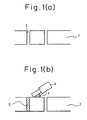
- a substrate 1 is perforated to thereby provide a hole 2, and subsequently, the present composition 3 is filled, using a squeezer 4, directly into the hole 2, and thereafter, the substrate thus-filled with the present composition is calcined at a predetermined temperature.
- the present composition 3 is filled into the hole 2 through a carrier film 5 of a green sheet covered by said film. Subsequently, the carrier film is removed, and two or more of thus-filled green sheets are laminated and the thus-obtained laminate calcined at a predetermined temperature.
- a ceramic substrate such as a glass ceramic composite substrate, an alumina substrate, a magnesia substrate or zirconia substrate are employed.
- a green sheet converted into one of the above substrates by a calcination thereof may be employed.
- the calcination temperature when a substrate is obtained from a green sheet is within the range of from 800 to 1000°C, e.g., for a glass ceramic substrate, and when AlN, ZrO2, and MgO green sheets are calcined, the calcination temperatures are, respectively, within the range of from 1600 to 1900°C.
- the calcination temperature is within the range of from 800 to 1000°C
- W or Mo is contained in the composition
- the calcination temperature is within the range of from 1500 to 1800°C.
- the calcination atmosphere for high melting point metals such as W and Mo, which are oxidized by calcination in an oxidizable atmosphere, and Cu etc. includes a nitrogen atmosphere, a nitrogen atmosphere containing steam, a nitrogen atmosphere containing hydrogen and steam, a reducing atmosphere containing hydrogen, or an inactive atmosphere, and for precious metal conductors of Au, Ag, Pd or Pt, appropriate oxidizable atmospheres such as the atmosphere are employed.
- the organometallic compound in the present invention since only a small amount of an organic binder and of an organic solvent need be added to the organometallic compound in the present invention, the amount of organic substances can be remarkably reduced compared with the conventional pastes. Therefore, the volume loss of paste is insignificant and the above problems of the conventional methods are solved, and thus dense vias free from gaps can be formed. Furthermore, the organometallic compound is converted into a metallic oxide or metallic nitride after calcination, resulting in an increase of the adhesion strength, as described above.
- organosilicic compound e.g. polysilazane
- the silicon compound and metallic powder are mixed, and if necessary, an amount of an organic binder and a solution are added to the obtained mixture.
- Polysilazane exhibits a function of an organic binder before the calcination of a substrate or the like, and is converted into amorphous Si3N4 after the calcination.
- an organosilicic compound functions as an organic binder, and the amount of organic substances can be noticeably reduced compared with the usual pastes. Therefore, the volume loss of the paste is insiginificant and the problems of the conventional methods are solved, and thus dense vias free from gaps can be formed.
- the thus-prepared tungsten paste was filled into holes with a diameter of 100 ⁇ m provided in a green sheet (containing 100 parts of AlN, 2 parts of CaCO3, PMMA binder and dibutyl phthalate) with a thickness of 300 ⁇ m and covered with a carrier film, through the film (Fig. 2).
- a green sheet containing 100 parts of AlN, 2 parts of CaCO3, PMMA binder and dibutyl phthalate
- a carrier film through the film (Fig. 2).
- Ten of these green sheets were laminated (50°C, 30 MPa), and after the binder was removed from the thus-prepared laminate in a nitrogen atmosphere at a temperature of 900°C, the laminate was calcinated in a nitrogen flow under 1 atm at a temperature of 1800°C for
- MEK methyl ethyl ketone
- the percentage composition (wt %) and volume ratio (vol %) of the prepared tungsten (W) paste are as set forth in the following Table 1.
- the tungsten paste prepared in Example 1 was employed.
- the tungsten paste was filled, using a squeezer, directly into holes with a diameter of 100 ⁇ m provided in an AlN substrate.
- the substrate was calcined in a nitrogen atmosphere at a temperature of 1700°C for 60 min.
- the thus-prepared copper paste was filled into holes with a diameter of 100 ⁇ m in a glass ceramic green sheet (containing 50 wt% of glass, 50 wt% of alumina, PMMA binder and dibutyl phthalate) with a thickness of 300 ⁇ m and covered with a carrier film, the filling being effected through said film (Fig. 2).
- Ten of these green sheets were laminated (130°C, 30 MPa), and after the thus-obtained laminate had been purged of binder in a nitrogen atmosphere at a temperature of 850°C, it was calcinated at a temperature of 1000°C.
- the percentage composition (wt %) and volume ratio (vol %) of the copper (Cu) paste prepared after the above low boiling solvent, methyl ethyl ketone, was volatilized, are as set forth in Table 5.
- Example 3 The copper paste prepared in Example 3 was employed. This copper paste was filled, using a squeezer, directly into the holes with a diameter of 100 ⁇ m in an alumina substrate (FGA substrate). The substrate was calcined for 10 min in a nitrogen atmosphere at a temperature of 1000°C.
- the thus-prepared copper paste was filled, using a squeezer, directly into the holes with a diameter of 100 ⁇ m in a ZrO2 substrate (Fig. 1), and after the substrate was dried, it was calcined in a nitrogen atmosphere at a temperature of 1000°C.
- terpeneol is the only liquid component of the prepared copper (Cu) paste, and thus a nearly powdered Cu paste composition is prepared.
- n-butylmagnesium chloride n-C4H9MgCl liquid
- 100 g of methyl ethyl ketone, 0.1 g of ethyl cellulose, and 5 g of terpeneol were mixed together
- 100 g of copper powder with a particle diameter of 0.5 ⁇ m were added to the obtained mixture
- the obtained mixture was kneaded by a kneader, and methyl ethyl ketone was volatilised, whereby a copper paste was prepared.
- the thus prepared copper paste was filled, using a squeezer, directly into the holes with a diameter of 100 ⁇ m provided on a MgO substrate (Fig. 1), and after the substrate was dried, it was calcined in a nitrogen atmosphere at a temperature of 1000°C.
- n-butylmagnesium chloride n-C4H9MgCl MW 116.873 is a brown liquid with a density (d) of 0.93.
- the components, composition etc. of the above copper paste are as set forth in Table 12.
- n-C4H9MgCl is the major constituent of the present copper paste.
- n-C4H9MgCl is reacted with H2O, CO2, CO, etc. to produce MgO. Then 20 g of n-C4H9MgCl, produces 6.897 g of MgO, and a copper conductor as set forth in Table 13 is formed in the holes for vias.
- the thus prepared copper powder was filled through said film (Fig. 2).
- Ten sheets of such green sheets were laminated (130°C, 30 MPa), and after the thus prepared laminate having been purged of binder in a nitrogen atmosphere at a temperature of 850°C, the laminate was calcinated at a temperature of 1000°C.
- MEK a low boiling solvent, is volatilized during the kneading, and the percentage composition of the prepared copper powder composition is as set forth in Table 14.
- Example 7 The copper powder prepared in Example 7 was employed. This copper powder was filled, using a squeezer, directly into an alumina substrate (FGA substrate) in which holes with a diameter of 100 ⁇ m are bored. This substrate was calcined in a nitrogen atmosphere at a temperature of 1000°C for 10 min.
- FGA substrate alumina substrate
- the thus prepared copper paste was filled through said film (Fig. 2).
- Ten sheets of such green sheets were laminated (130°C, 30 MPa), and after the thus prepared laminate had been purged of binder in a nitrogen atmosphere at a temperature of 850°C, the laminae was calcinated at a temperature of 1000°C.
- nonamethyltrisilazane [(CH3)3Si]3N is in the form of white crystals at normal temperature, and MEK, a low boiling point solvent, is volatilized when kneaded, so that a powdered composition is obtained.
- MEK a low boiling point solvent
- [(CH3)3Si]3N contained in the W powder composition is heat decomposed in a nitrogen atmosphere and Si3N4, an inorganic substance, is produced as shown in the above reaction formula (5).
- the present composition for the formation of vias is composed of a certain kind of metallic powder and 5 to 40 wt%, based on the weight of said metallic powder, of an organometallic compound or in addition thereto, a heat decomposable organic binder and a high boiling point organic solvent, the present composition has little volume loss after calcination when filled into the holes of a substrate, and thus, with the present composition, it becomes possible to form dense vias free from gaps.
- the adhesion strength between a substrate and a conductor can be improved by using the present composition because, after the calcination of the substrate, the coefficient of the substrate is approximately that of the conductor or because an organometallic compound of the present composition is converted into a metallic oxide or a metallic nitride.
Landscapes
- Engineering & Computer Science (AREA)
- Chemical & Material Sciences (AREA)
- Microelectronics & Electronic Packaging (AREA)
- Dispersion Chemistry (AREA)
- Inorganic Chemistry (AREA)
- Manufacturing & Machinery (AREA)
- Parts Printed On Printed Circuit Boards (AREA)
- Conductive Materials (AREA)
Abstract
Composition céramique de formation d'interconnexions. Afin de résoudre le problème du vide se produisant dans l'interface entre le conducteur et le substrat, dû à un remplissage insuffisant des interconnexions provoquées par la réduction du volume lors de la formation d'interconnexions, et afin de résoudre le problème de la mauvaise adhérence entre le conducteur et le substrat, la composition de formation d'interconnexions en céramique comprend les composants suivants (a) et (b): (a) au moins une poudre métallique ou une poudre d'alliage choisie parmi la poudre métallique de cuivre, or, argent, tungstène, molibdène, nickel, paradium, platine ou aluminium, ou leur poudre d'alliage; et (b) un composé organométallique d'un composé de silicium organique, d'un composé d'aluminium organique, d'un composé de zirconium organique ou d'un composé de magnésium organique, en une quantité comprise entre 5 et 40 % en poids par rapport à la poudre métallique ou à la poudre d'alliage précitée. En plus des composants (a) et (b) précités, la composition de formation de connexions de l'invention contient les composants suivants (c) et (d): (c) un dérivé de cellulose ou un liant organique à décomposition thermique du type acrylate de polymétaméthyle; et (d) un solvant organique à pointe d'ébullition élevée. Le procédé de formation d'interconnexion dans le substrat céramique consiste à former un trou dans un substrat céramique, tel qu'un substrat composite en verre-céramique, un substrat en oxyde d'aluminium, un substrat en magnésie, un substrat en zircone, ou une feuille verte de ceux-ci, et à former le trou ainsi réalisé à l'aide de n'importe laquelle desdites compositions, et un procédé à la cuisson.
Applications Claiming Priority (2)
| Application Number | Priority Date | Filing Date | Title |
|---|---|---|---|
| JP240684/89 | 1989-09-19 | ||
| JP24068489 | 1989-09-19 |
Publications (2)
| Publication Number | Publication Date |
|---|---|
| EP0444216A1 true EP0444216A1 (fr) | 1991-09-04 |
| EP0444216A4 EP0444216A4 (en) | 1992-04-08 |
Family
ID=17063168
Family Applications (1)
| Application Number | Title | Priority Date | Filing Date |
|---|---|---|---|
| EP19900913894 Withdrawn EP0444216A4 (en) | 1989-09-19 | 1990-09-19 | Via-forming ceramics composition |
Country Status (3)
| Country | Link |
|---|---|
| US (1) | US5443786A (fr) |
| EP (1) | EP0444216A4 (fr) |
| WO (1) | WO1991004650A1 (fr) |
Cited By (3)
| Publication number | Priority date | Publication date | Assignee | Title |
|---|---|---|---|---|
| EP0536862A1 (fr) * | 1991-10-11 | 1993-04-14 | W.R. Grace & Co.-Conn. | Procédé pour fabriquer des rainures enternées |
| EP0670598A3 (fr) * | 1994-03-03 | 1996-04-10 | Shinko Electric Ind Co | Carte de circuit céramique et procédé de fabrication. |
| EP0690505A3 (fr) * | 1994-07-01 | 1996-08-07 | Shinko Electric Ind Co | Matériau fritté substrat céramique et sa fabricating |
Families Citing this family (13)
| Publication number | Priority date | Publication date | Assignee | Title |
|---|---|---|---|---|
| JP2762017B2 (ja) * | 1993-06-14 | 1998-06-04 | ニッコー株式会社 | スルーホールを充填したセラミック基板およびスルーホール充填用導体ペースト |
| US6288347B1 (en) * | 1997-05-30 | 2001-09-11 | Kyocera Corporation | Wiring board for flip-chip-mounting |
| DE19824783A1 (de) | 1998-06-03 | 1999-12-16 | Siemens Ag | Vorrichtung zur Formung eines Elektronenstrahls, Verfahren zur Herstellung der Vorrichtung und Anwendung |
| JP2000244123A (ja) * | 1999-02-19 | 2000-09-08 | Hitachi Ltd | 多層セラミック回路基板 |
| US6248680B1 (en) | 1999-06-01 | 2001-06-19 | Alliedsignal, Inc. | Low temperature burnout screen printing frit vehicles and pastes |
| US6749775B2 (en) * | 2002-01-29 | 2004-06-15 | Cts Corporation | Conductive via composition |
| DE112006002464T5 (de) * | 2005-09-14 | 2008-07-24 | Littelfuse, Inc., Des Plaines | Gasgefüllter Überspannungsableiter, aktivierende Verbindung, Zündstreifen und Herstellungsverfahren dafür |
| US20100124602A1 (en) * | 2008-11-18 | 2010-05-20 | Palo Alto Research Center Incorporated | Easily flowing inks for extrusion |
| US9892816B2 (en) * | 2013-06-27 | 2018-02-13 | Heraeus Precious Metals North America Conshohocken Llc | Platinum containing conductive paste |
| CN104064478B (zh) * | 2014-06-24 | 2016-08-31 | 南京航空航天大学 | 一种铜/氮化铝陶瓷复合导热基板的制作方法 |
| JP6433351B2 (ja) * | 2015-03-19 | 2018-12-05 | 株式会社ノリタケカンパニーリミテド | 被覆銅粉末、銅ペースト、および銅導体膜 |
| CN104916547B (zh) * | 2015-05-04 | 2018-06-19 | 山东航天电子技术研究所 | 一种溢出式成膜基板通柱填充方法 |
| CN116731636B (zh) * | 2023-07-11 | 2026-04-14 | 中科意创(广州)科技有限公司 | 一种贴片胶水及其贴片工艺 |
Family Cites Families (9)
| Publication number | Priority date | Publication date | Assignee | Title |
|---|---|---|---|---|
| JPS5824037B2 (ja) * | 1980-05-26 | 1983-05-18 | 富士通株式会社 | 導体ボ−ル配列方法 |
| JPS6084711A (ja) * | 1983-10-14 | 1985-05-14 | 株式会社日立製作所 | スル−ホ−ル充填用ペ−スト |
| US4599277A (en) * | 1984-10-09 | 1986-07-08 | International Business Machines Corp. | Control of the sintering of powdered metals |
| US4885038A (en) * | 1986-05-01 | 1989-12-05 | International Business Machines Corporation | Method of making multilayered ceramic structures having an internal distribution of copper-based conductors |
| CA1273853A (fr) * | 1986-12-17 | 1990-09-11 | Hitoshi Suzuki | Methode de production d'une carte ceramique a circuit |
| JPS6454613A (en) * | 1987-08-25 | 1989-03-02 | Catalysts & Chem Ind Co | Application liquid for forming transparent superconductive film and manufacture thereof |
| JPS6438905A (en) * | 1987-08-04 | 1989-02-09 | Mitsubishi Electric Corp | Thick film paste material |
| JPS6481106A (en) * | 1987-09-22 | 1989-03-27 | Sumitomo Metal Mining Co | Composition for forming conductive film |
| US4954926A (en) * | 1989-07-28 | 1990-09-04 | E. I. Du Pont De Nemours And Company | Thick film conductor composition |
-
1990
- 1990-09-19 US US07/700,163 patent/US5443786A/en not_active Expired - Fee Related
- 1990-09-19 EP EP19900913894 patent/EP0444216A4/en not_active Withdrawn
- 1990-09-19 WO PCT/JP1990/001202 patent/WO1991004650A1/fr not_active Ceased
Cited By (6)
| Publication number | Priority date | Publication date | Assignee | Title |
|---|---|---|---|---|
| EP0536862A1 (fr) * | 1991-10-11 | 1993-04-14 | W.R. Grace & Co.-Conn. | Procédé pour fabriquer des rainures enternées |
| EP0670598A3 (fr) * | 1994-03-03 | 1996-04-10 | Shinko Electric Ind Co | Carte de circuit céramique et procédé de fabrication. |
| US5702807A (en) * | 1994-03-03 | 1997-12-30 | Shiko Electric Industries Co., Ltd. | Ceramic circuit board and manufacturing method thereof |
| EP0690505A3 (fr) * | 1994-07-01 | 1996-08-07 | Shinko Electric Ind Co | Matériau fritté substrat céramique et sa fabricating |
| US5997999A (en) * | 1994-07-01 | 1999-12-07 | Shinko Electric Industries Co., Ltd. | Sintered body for manufacturing ceramic substrate |
| EP1005088A1 (fr) * | 1994-07-01 | 2000-05-31 | Shinko Electric Industries Co. Ltd. | Matériau fritté substrat céramique et sa fabrication |
Also Published As
| Publication number | Publication date |
|---|---|
| US5443786A (en) | 1995-08-22 |
| EP0444216A4 (en) | 1992-04-08 |
| WO1991004650A1 (fr) | 1991-04-04 |
Similar Documents
| Publication | Publication Date | Title |
|---|---|---|
| EP0444216A1 (fr) | Composition ceramique de formation d'interconnexions | |
| US4961987A (en) | Aluminum nitride sintered body with high thermal conductivity and process for producing same | |
| EP2544515A1 (fr) | Procédé de fabrication d'un substrat métallisé | |
| EP0306270A1 (fr) | Compositions conductrices en couche épaisse pour utilisation avec un substrat de nitrure d'aluminium | |
| US5294388A (en) | Heat conductive colored aluminum nitride sintered body and method of preparing the same | |
| DE69812533T2 (de) | Aluminiumnitridsubstrat und Verfahren zu dessen Herstellung | |
| JPH0393683A (ja) | 銅ペースト及びそれを用いたメタライズ方法 | |
| EP0764618A2 (fr) | Compositions pâteuses conductrices en couche épaisse pour des substrats de nitrure d'aluminium | |
| JPH08161930A (ja) | 導電ペースト並びにそれを用いた導電体および多層セラミック基板 | |
| US5766305A (en) | Metal powder composition for metallization and a metallized substrate | |
| EP1434750B1 (fr) | Compositions de conducteur en couche epaisse utilisables sur des substrats de nitrure d'aluminium | |
| JP2000244123A (ja) | 多層セラミック回路基板 | |
| JP7317397B2 (ja) | 酸化銅ペースト及び電子部品の製造方法 | |
| EP0433992B1 (fr) | Procédé de formation d'une couche métallisée sur un corps fritté de nitrure d'aluminium | |
| KR930011602B1 (ko) | 세라믹스의 비아 형성용 조성물 | |
| CA1165994A (fr) | Compositions conductrices en couche epaisse | |
| JP2002176236A (ja) | ビアホール導体用組成物ならびに多層セラミック基板およびその製造方法 | |
| JP3150932B2 (ja) | セラミック多層回路基板用導電ペースト | |
| JP4012601B2 (ja) | 銅メタライズ組成物及びそれを用いたガラスセラミック配線基板 | |
| JPH05156303A (ja) | メタライズ用金属粉末組成物,それを用いたメタライズ基板及びメタライズ基板の製造方法 | |
| JP2550630B2 (ja) | 導電性被膜形成用銅ペースト | |
| JPH10233119A (ja) | 銅導体ペースト及び該銅導体ペーストを印刷した基板 | |
| JPWO1991004650A1 (ja) | セラミックスのビア形成用組成物 | |
| JP3420424B2 (ja) | 配線基板 | |
| JP3505659B2 (ja) | 導電膜付メタライズ基板の製造方法 |
Legal Events
| Date | Code | Title | Description |
|---|---|---|---|
| PUAI | Public reference made under article 153(3) epc to a published international application that has entered the european phase |
Free format text: ORIGINAL CODE: 0009012 |
|
| 17P | Request for examination filed |
Effective date: 19910528 |
|
| AK | Designated contracting states |
Kind code of ref document: A1 Designated state(s): DE FR GB |
|
| A4 | Supplementary search report drawn up and despatched |
Effective date: 19920220 |
|
| AK | Designated contracting states |
Kind code of ref document: A4 Designated state(s): DE FR GB |
|
| 17Q | First examination report despatched |
Effective date: 19940926 |
|
| STAA | Information on the status of an ep patent application or granted ep patent |
Free format text: STATUS: THE APPLICATION IS DEEMED TO BE WITHDRAWN |
|
| 18D | Application deemed to be withdrawn |
Effective date: 19980121 |