EP0444363A2 - Intégration d'impulsion de courant - Google Patents
Intégration d'impulsion de courant Download PDFInfo
- Publication number
- EP0444363A2 EP0444363A2 EP90314391A EP90314391A EP0444363A2 EP 0444363 A2 EP0444363 A2 EP 0444363A2 EP 90314391 A EP90314391 A EP 90314391A EP 90314391 A EP90314391 A EP 90314391A EP 0444363 A2 EP0444363 A2 EP 0444363A2
- Authority
- EP
- European Patent Office
- Prior art keywords
- current
- integration
- state
- output
- integration amplifier
- Prior art date
- Legal status (The legal status is an assumption and is not a legal conclusion. Google has not performed a legal analysis and makes no representation as to the accuracy of the status listed.)
- Granted
Links
Images

Classifications
-
- G—PHYSICS
- G06—COMPUTING OR CALCULATING; COUNTING
- G06G—ANALOGUE COMPUTERS
- G06G7/00—Devices in which the computing operation is performed by varying electric or magnetic quantities
- G06G7/12—Arrangements for performing computing operations, e.g. operational amplifiers specially adapted therefor
- G06G7/18—Arrangements for performing computing operations, e.g. operational amplifiers specially adapted therefor for integration or differentiation; for forming integrals
- G06G7/184—Arrangements for performing computing operations, e.g. operational amplifiers specially adapted therefor for integration or differentiation; for forming integrals using capacitive elements
- G06G7/186—Arrangements for performing computing operations, e.g. operational amplifiers specially adapted therefor for integration or differentiation; for forming integrals using capacitive elements using an operational amplifier comprising a capacitor or a resistor in the feedback loop
-
- H—ELECTRICITY
- H03—ELECTRONIC CIRCUITRY
- H03L—AUTOMATIC CONTROL, STARTING, SYNCHRONISATION OR STABILISATION OF GENERATORS OF ELECTRONIC OSCILLATIONS OR PULSES
- H03L7/00—Automatic control of frequency or phase; Synchronisation
- H03L7/06—Automatic control of frequency or phase; Synchronisation using a reference signal applied to a frequency- or phase-locked loop
- H03L7/08—Details of the phase-locked loop
- H03L7/085—Details of the phase-locked loop concerning mainly the frequency- or phase-detection arrangement including the filtering or amplification of its output signal
- H03L7/089—Details of the phase-locked loop concerning mainly the frequency- or phase-detection arrangement including the filtering or amplification of its output signal the phase or frequency detector generating up-down pulses
- H03L7/0891—Details of the phase-locked loop concerning mainly the frequency- or phase-detection arrangement including the filtering or amplification of its output signal the phase or frequency detector generating up-down pulses the up-down pulses controlling source and sink current generators, e.g. a charge pump
- H03L7/0895—Details of the current generators
- H03L7/0896—Details of the current generators the current generators being controlled by differential up-down pulses
Definitions
- This invention relates to current-pulse integrators that generate voltage signals proportional to the integral of a current over a pulse-width time.
- Current-pulse integrators typically include an integration amplifier having an integration capacitor connected between the input and the output of the integration amplifier. A set of current switches cause current to pass through the integration capacitor in one direction when the capacitor is being charged, and cause current to pass through the capacitor in the opposite direction when the capacitor is being discharged. The voltage across the integration capacitor is equal to the product of the current and the charging time, minus the product of the current and the discharging time.
- the invention features a current pulse integrator that includes an integration amplifier having an integration capacitor located in its feedback loop.
- the current pulse integrator also includes switching circuitry, which causes current to pass through the feedback integration capacitor in a first direction during a first state of operation of the current pulse integrator, and which prevents current from passing through the integration capacitor in the first direction during at least one other state of operation of the current pulse integrator.
- the output current of the integration amplifier remains unchanged as the switching circuitry switches between the first state of operation and the other state or states of operation.
- the switching circuitry provides a path through the feedback loop for the output current of the integration amplifier to pass through the integration capacitor during the first state of operation.
- the switching circuitry also provides an alternative, nonfeedback path for the output current of the integration amplifier during the other state or states of operation.
- the current pulse integrator includes three current sources, and the switching circuitry includes four current switches.
- a first current switch is located between a first current source and a second current source.
- a second current switch is located between the output of the integration amplifier and the second current source.
- a third current switch has one end connected to the first current source and the input to the integration amplifier, and the other end connected to the third current source.
- a fourth current switch is connected between the output of the integration amplifier and the third current source.
- the second current switch is controlled by a discharge pulse signal
- the first current switch is controlled by a signal that is inverse to the discharge signal
- the third current switch is controlled by a charge pulse signal
- the fourth current switch is controlled by a signal that is inverse to the charge signal.
- the current pulse integrator has a charge state, a discharge state, an off state, and an on state of operation. In the charge state the charge signal is high and the discharge signal is low, and current passes through the integration capacitor in a direction from the output of the integration amplifier to the input of the integration amplifier, to charge the integration capacitor. In the discharge state the discharge signal is high and the charge signal is low, and current passes through the integration capacitor in a direction from the input of the integration amplifier to the output of the integration amplifier, to discharge the integration capacitor. In the off state the charge signal and the discharge signal are low, and no current flows through the integration capacitor. In the on state the charge signal and the discharge signal are high, and no current flows through the integration capacitor.
- the charge state current flows from the first current source through the first current switch to the second current source, and current flows from the output of the integration amplifier through the integration capacitor and through the third current switch to the third current source.
- the discharge state current flows from the first current source through the integration capacitor and through the second and fourth current switches to the second and third current sources, and current flows from the output of the integration amplifier through the second and fourth current switches to the second and third current sources.
- the off state current flows from the first current source through the first current switch to the second current source, and current flows from the output of the integration amplifier through the fourth current switch to the third current source.
- the on state current flows from the first current source through the third current switch to the third current source, and current flows from the output of the integration amplifier through the second current switch to the second current source.
- Current pulse integrators according to the invention have an integration amplifier whose output current remains unchanged as the switching circuitry switches between the various states of operation of the circuit.
- the integrator circuit can therefore exhibit a high degree of accuracy, even where changes between the various states of operation occur frequently.
- a phase detector produces the charge and discharge pulse signals, which are received by the current pulse integrator.
- a voltage-controlled oscillator produces a feedback signal having a frequency of oscillation that is proportional to the charge across the integration capacitor of the current-pulse integrator. The feedback signal is received by the phase detector.
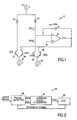
- Figure 1 is a circuit diagram of a current pulse integrator according to the invention.
- Figure 2 is a block diagram of a phase-locked loop circuit that utilizes a current pulse integrator according to the invention.
- Figures 3A, 3B, and 3C are pulse diagrams of input pulses to the phase-locked loop circuit of Figure 2, DISCHARGE pulses produced by the phase-locked loop circuit, and CHARGE pulses produced by the phase-locked loop circuit, respectively.
- a high-speed current-pulse integrator circuit 10 has an integration amplifier 12 and an integration capacitor 14 located in the feedback loop of the integration amplifier 12.
- the voltage across the integration capacitor is the integral of a current over a set of CHARGE pulse widths, minus the integral of the current over a set of DISCHARGE pulse widths.
- the current through the integration capacitor is controlled by three current sources 16, 18, and 20, and by switching circuitry that includes four high-speed current switches 22, 24, 26, and 28, which may be npn transistors, and two high-speed Schottky diodes 30 and 32.
- Diode 30 connects current source 16 with current switch 22, which is connected to current source 18.
- Diode 32 connects current source 16 with the inverting input of integration amplifier 12 and also with current switch 26, which is connected to current source 20.
- Current switch 24 connects the output of integration amplifier 12 with current source 18.
- Current switch 28 connects the output of integration amplifier 12 with current source 20.
- the four current switches 22, 24, 26, and 28 are regulated by pulse signals DIS , DIS, CHG, and CHG respectively.
- the circuit has four states of operation: OFF, DISCHARGE, CHARGE, and ON.
- CHARGE a current of magnitude I flows through the integration capacitor 14 to the left in Figure 1.
- DISCHARGE a current of magnitude I flows through the integration capacitor to the right in Figure 1.
- no current flows through the integration capacitor.
- the CHG and DIS pulse signals are set low, while the CHG and DIS pulse signals are set high, causing current switches 22 and 28 to turn on and current switches 24 and 26 to turn off.
- Current of magnitude I flows from current source 16, through diode 30 and current switch 22, to current source 18.
- Current source 20 pulls a current of magnitude I out of the output of integration amplifier 12 and through current switch 28. No current flows through integration capacitor 14.
- the CHG and DIS pulse signals are set low, while the CHG and DIS pulse signals are set high, causing current switches 24 and 28 to turn on and current switches 22 and 26 to turn off.
- Current of magnitude I flows from current source 16, through diode 32 and capacitor 14, through current switches 24 and 28, to current sources 18 and 20.
- a current of magnitude I flows out of the output of integration amplifier 12, through current switches 24 and 28, to current sources 18 and 20.
- the CHG and DIS pulse signals are set low, while the CHG and DIS pulse signals are set high, causing current switches 22 and 26 to turn on and current switches 24 and 28 to turn off.
- Current of magnitude I flows from current source 16, through diode 30 and current switch 22, to current source 18.
- Current source 20 pulls a current of magnitude I out of the output of integration amplifier 12 and through capacitor 14 and current switch 26.
- the CHG and DIS pulse signals are set low, while the CHG and DIS pulse signals are set high, causing current switches 24 and 26 to turn on and current switches 22 and 28 to turn off.
- Current of magnitude I flows from current source 16, through diode 32 and current switch 26, to current source 20.
- Current source 18 pulls a current of magnitude I out of the output of integration amplifier 12 and through current switch 24. No current flows through integration capacitor 14.
- the integration amplifier 12 requires a certain settling time for the output current of the integration amplifier to settle from an original value to within a specified percentage of a final value. Yet, the output current of the integration amplifier 12 remains a constant current of magnitude I regardless of the state of operation of the circuit. Thus, as the circuit switches to the CHARGE or DISCHARGE state of operation, current of magnitude I immediately passes through the capacitor 14 in the appropriate direction, without any delay due to the integration amplifier 12 adjusting its output current. The accuracy of integration is thereby improved, especially where changes between the CHARGE state and the DISCHARGE state of operation occur frequently.
- the current switches 22, 24, 26, and 28 and the Schottky diodes 30 and 32 have a fast response time.
- the integration amplifier 12 can slew its output voltage to track the changing voltage of the integration capacitor 14 as fast as the bandwidth limitation of the integration amplifier 12 allows. Although the frequency response time (the speed) of the integration amplifier is limited by the bandwidth limitation, the deterioration in current passing through the integration capacitor 14 due to the limited frequency response time of the integration amplifier 12 is minimal.
- FIG. 2 shows a phase-locked loop circuit 34 that utilizes a current-pulse integrator 10 according to the invention.
- a phase detector 36 receives an input signal pulse train, shown in Figure 3A, and a feedback signal pulse train.
- Phase detector 36 produces a train of DISCHARGE pulses, shown in Figure 3B, that rise and fall in synchronization with the feedback signal.
- Phase detector 36 also produces a train of CHARGE pulses, shown in Figure 3C, that rise in synchronization with the rising of the input signal pulses shown in Figure 3A, and that fall in synchronization with the falling of the DISCHARGE pulses shown in FIGURE 3B.
- the CHARGE pulses of Figure 3C are narrower than the DISCHARGE pulses of Figure 3B.
- the CHARGE pulses of Figure 3C are wider than the DISCHARGE pulses of Figure 3B.
- the current pulse integrator 10 produces a voltage V cap across its integration capacitor that is proportional to the integral of current I over the durations of the CHG pulse signals, minus the integral of current I over the durations of the DIS pulse signals.
- a voltage-controlled oscillator 38 receives the voltage across the integration capacitor and produces the feedback signal with a frequency of oscillation that is proportional to the voltage across the integration capacitor. The feedback signal locks onto the frequency of the input signal.
Landscapes
- Engineering & Computer Science (AREA)
- Physics & Mathematics (AREA)
- Mathematical Physics (AREA)
- Theoretical Computer Science (AREA)
- Power Engineering (AREA)
- Software Systems (AREA)
- Computer Hardware Design (AREA)
- General Physics & Mathematics (AREA)
- Stabilization Of Oscillater, Synchronisation, Frequency Synthesizers (AREA)
- Amplifiers (AREA)
- Analogue/Digital Conversion (AREA)
- Manipulation Of Pulses (AREA)
Applications Claiming Priority (2)
| Application Number | Priority Date | Filing Date | Title |
|---|---|---|---|
| US485151 | 1990-02-26 | ||
| US07/485,151 US5093628A (en) | 1990-02-26 | 1990-02-26 | Current-pulse integrating circuit and phase-locked loop |
Publications (3)
| Publication Number | Publication Date |
|---|---|
| EP0444363A2 true EP0444363A2 (fr) | 1991-09-04 |
| EP0444363A3 EP0444363A3 (en) | 1992-04-01 |
| EP0444363B1 EP0444363B1 (fr) | 1997-07-16 |
Family
ID=23927082
Family Applications (1)
| Application Number | Title | Priority Date | Filing Date |
|---|---|---|---|
| EP90314391A Expired - Lifetime EP0444363B1 (fr) | 1990-02-26 | 1990-12-28 | Intégration d'impulsion de courant |
Country Status (5)
| Country | Link |
|---|---|
| US (1) | US5093628A (fr) |
| EP (1) | EP0444363B1 (fr) |
| JP (1) | JPH0575411A (fr) |
| CA (1) | CA2034127C (fr) |
| DE (1) | DE69031070T2 (fr) |
Families Citing this family (1)
| Publication number | Priority date | Publication date | Assignee | Title |
|---|---|---|---|---|
| US11216723B2 (en) | 2017-08-11 | 2022-01-04 | Syntiant | Pulse-width modulated multiplier |
Family Cites Families (12)
| Publication number | Priority date | Publication date | Assignee | Title |
|---|---|---|---|---|
| US4032768A (en) * | 1975-10-24 | 1977-06-28 | Tektronix, Inc. | Constant velocity vector generator |
| US4034309A (en) * | 1975-12-23 | 1977-07-05 | International Business Machines Corporation | Apparatus and method for phase synchronization |
| DE2600194C3 (de) * | 1976-01-05 | 1978-08-24 | Varian Mat Gmbh, 2800 Bremen | Entladungsschaltung für den Integrationskondensator eines kapazitiv gegengekoppelten Integrationsverstärkers |
| US3988595A (en) * | 1976-01-19 | 1976-10-26 | Fairchild Camera And Instrument Corporation | High-gain differential input comparator with emitter feedback input hysteresis |
| US4074205A (en) * | 1977-03-09 | 1978-02-14 | Rca Corporation | Input stage for fast-slewing amplifier |
| DE2737432C3 (de) * | 1977-08-19 | 1980-03-06 | Hewlett-Packard Gmbh, 7030 Boeblingen | Integratorschaltung mit Begrenzung |
| US4374335A (en) * | 1980-05-19 | 1983-02-15 | Precision Monolithics, Inc. | Tuneable I.C. active integrator |
| JPS585873A (ja) * | 1981-07-03 | 1983-01-13 | Toshiba Corp | スイツチドキヤパシタ積分器 |
| DE3408220A1 (de) * | 1984-03-07 | 1985-09-12 | Telefunken electronic GmbH, 7100 Heilbronn | Steuerbarer integrator |
| IT1186340B (it) * | 1985-10-29 | 1987-11-26 | Sgs Microelettronica Spa | Integratore differenziale a condensatore commutato utilizzante un unico condensatore di integrazione |
| US4918338A (en) * | 1988-10-04 | 1990-04-17 | North American Philips Corporation | Drain-biassed transresistance device for continuous time filters |
| US4885553A (en) * | 1988-11-30 | 1989-12-05 | Motorola, Inc. | Continuously adaptive phase locked loop synthesizer |
-
1990
- 1990-02-26 US US07/485,151 patent/US5093628A/en not_active Expired - Lifetime
- 1990-12-28 EP EP90314391A patent/EP0444363B1/fr not_active Expired - Lifetime
- 1990-12-28 DE DE69031070T patent/DE69031070T2/de not_active Expired - Fee Related
-
1991
- 1991-01-14 CA CA002034127A patent/CA2034127C/fr not_active Expired - Fee Related
- 1991-02-21 JP JP3027393A patent/JPH0575411A/ja active Pending
Also Published As
| Publication number | Publication date |
|---|---|
| US5093628A (en) | 1992-03-03 |
| CA2034127C (fr) | 1995-10-03 |
| JPH0575411A (ja) | 1993-03-26 |
| EP0444363B1 (fr) | 1997-07-16 |
| CA2034127A1 (fr) | 1991-08-27 |
| DE69031070T2 (de) | 1997-12-04 |
| EP0444363A3 (en) | 1992-04-01 |
| DE69031070D1 (de) | 1997-08-21 |
Similar Documents
| Publication | Publication Date | Title |
|---|---|---|
| EP0503571B1 (fr) | Amplificateur à modulation de largeur d'impulsion | |
| EP0805553B1 (fr) | Oscillateur contrÔlé par une tension et circuit à verrouillage de phase comportant cet oscillateur | |
| US6392494B2 (en) | Frequency comparator and clock regenerating device using the same | |
| US5363419A (en) | Dual phase-locked-loop having forced mid range fine control zero at handover | |
| US5740213A (en) | Differential charge pump based phase locked loop or delay locked loop | |
| US5218315A (en) | Switching amplifier | |
| US5028888A (en) | Multistage current-controlled oscillator | |
| EP0731560B1 (fr) | Oscillateur commandé en tension à large gamme de fréquence et à faible sautillement | |
| DE69902838T2 (de) | Schaltungsanordnung für einen Phasenkomparator | |
| EP0249665B1 (fr) | Oscillateur déclenché commandé en tension utilisant une porte à recouvrement rapide | |
| US6124746A (en) | Adjustable delay circuit | |
| GB2274718A (en) | CMOS peak amplitude detector | |
| EP0330280B1 (fr) | Oscillateur commandé par une tension | |
| US5929671A (en) | Waveform generator | |
| EP0880824A1 (fr) | Circuits de reduction du bruit de phase | |
| US5093628A (en) | Current-pulse integrating circuit and phase-locked loop | |
| US4829268A (en) | Loop filter for frequency multiplying phase locked loop | |
| US3317756A (en) | Signal integrating apparatus | |
| EP0745288B1 (fr) | Boucle a phase asservie pour signaux a formes d'ondes rectangulaires | |
| US4121170A (en) | Tunable oscillator with high stability and accurate frequency | |
| US6466097B1 (en) | Phase locked loop and associated control method | |
| US5724008A (en) | Phase-locked loop with charge distribution | |
| US5168247A (en) | Oscillator and voltage-to-frequency coverter employing the same | |
| US4554464A (en) | Propagation delay generator | |
| US3388340A (en) | Phase controlled ring oscillator comprising a plurality of active delay stages individually coupled to a control device |
Legal Events
| Date | Code | Title | Description |
|---|---|---|---|
| PUAI | Public reference made under article 153(3) epc to a published international application that has entered the european phase |
Free format text: ORIGINAL CODE: 0009012 |
|
| 17P | Request for examination filed |
Effective date: 19910102 |
|
| AK | Designated contracting states |
Kind code of ref document: A2 Designated state(s): DE FR GB IT |
|
| PUAL | Search report despatched |
Free format text: ORIGINAL CODE: 0009013 |
|
| AK | Designated contracting states |
Kind code of ref document: A3 Designated state(s): DE FR GB IT |
|
| RAP1 | Party data changed (applicant data changed or rights of an application transferred) |
Owner name: QUANTUM CORPORATION |
|
| 17Q | First examination report despatched |
Effective date: 19960314 |
|
| GRAG | Despatch of communication of intention to grant |
Free format text: ORIGINAL CODE: EPIDOS AGRA |
|
| GRAH | Despatch of communication of intention to grant a patent |
Free format text: ORIGINAL CODE: EPIDOS IGRA |
|
| GRAH | Despatch of communication of intention to grant a patent |
Free format text: ORIGINAL CODE: EPIDOS IGRA |
|
| GRAA | (expected) grant |
Free format text: ORIGINAL CODE: 0009210 |
|
| AK | Designated contracting states |
Kind code of ref document: B1 Designated state(s): DE FR GB IT |
|
| REF | Corresponds to: |
Ref document number: 69031070 Country of ref document: DE Date of ref document: 19970821 |
|
| ET | Fr: translation filed | ||
| ITF | It: translation for a ep patent filed | ||
| PLBE | No opposition filed within time limit |
Free format text: ORIGINAL CODE: 0009261 |
|
| STAA | Information on the status of an ep patent application or granted ep patent |
Free format text: STATUS: NO OPPOSITION FILED WITHIN TIME LIMIT |
|
| 26N | No opposition filed | ||
| PGFP | Annual fee paid to national office [announced via postgrant information from national office to epo] |
Ref country code: FR Payment date: 19981202 Year of fee payment: 9 |
|
| PG25 | Lapsed in a contracting state [announced via postgrant information from national office to epo] |
Ref country code: FR Free format text: LAPSE BECAUSE OF NON-PAYMENT OF DUE FEES Effective date: 20000831 |
|
| REG | Reference to a national code |
Ref country code: FR Ref legal event code: ST |
|
| PGFP | Annual fee paid to national office [announced via postgrant information from national office to epo] |
Ref country code: GB Payment date: 20001201 Year of fee payment: 11 |
|
| PGFP | Annual fee paid to national office [announced via postgrant information from national office to epo] |
Ref country code: DE Payment date: 20001211 Year of fee payment: 11 |
|
| PG25 | Lapsed in a contracting state [announced via postgrant information from national office to epo] |
Ref country code: GB Free format text: LAPSE BECAUSE OF NON-PAYMENT OF DUE FEES Effective date: 20011228 |
|
| REG | Reference to a national code |
Ref country code: GB Ref legal event code: IF02 |
|
| PG25 | Lapsed in a contracting state [announced via postgrant information from national office to epo] |
Ref country code: DE Free format text: LAPSE BECAUSE OF NON-PAYMENT OF DUE FEES Effective date: 20020702 |
|
| GBPC | Gb: european patent ceased through non-payment of renewal fee |
Effective date: 20011228 |
|
| PG25 | Lapsed in a contracting state [announced via postgrant information from national office to epo] |
Ref country code: IT Free format text: LAPSE BECAUSE OF NON-PAYMENT OF DUE FEES;WARNING: LAPSES OF ITALIAN PATENTS WITH EFFECTIVE DATE BEFORE 2007 MAY HAVE OCCURRED AT ANY TIME BEFORE 2007. THE CORRECT EFFECTIVE DATE MAY BE DIFFERENT FROM THE ONE RECORDED. Effective date: 20051228 |