EP0444366B1 - Laser à semi-conducteur avec une section à rainure de forme mésa inverse - Google Patents
Laser à semi-conducteur avec une section à rainure de forme mésa inverse Download PDFInfo
- Publication number
- EP0444366B1 EP0444366B1 EP90314466A EP90314466A EP0444366B1 EP 0444366 B1 EP0444366 B1 EP 0444366B1 EP 90314466 A EP90314466 A EP 90314466A EP 90314466 A EP90314466 A EP 90314466A EP 0444366 B1 EP0444366 B1 EP 0444366B1
- Authority
- EP
- European Patent Office
- Prior art keywords
- layer
- cladding layer
- current
- cladding
- etching
- Prior art date
- Legal status (The legal status is an assumption and is not a legal conclusion. Google has not performed a legal analysis and makes no representation as to the accuracy of the status listed.)
- Expired - Lifetime
Links
- 239000004065 semiconductor Substances 0.000 title claims description 54
- 238000005253 cladding Methods 0.000 claims description 74
- 238000005530 etching Methods 0.000 claims description 61
- 238000000034 method Methods 0.000 claims description 33
- 230000003287 optical effect Effects 0.000 claims description 23
- 239000010409 thin film Substances 0.000 claims description 22
- 238000004519 manufacturing process Methods 0.000 claims description 16
- 239000000758 substrate Substances 0.000 claims description 15
- QAOWNCQODCNURD-UHFFFAOYSA-N Sulfuric acid Chemical compound OS(O)(=O)=O QAOWNCQODCNURD-UHFFFAOYSA-N 0.000 claims description 12
- 229910052782 aluminium Inorganic materials 0.000 claims description 9
- XAGFODPZIPBFFR-UHFFFAOYSA-N aluminium Chemical compound [Al] XAGFODPZIPBFFR-UHFFFAOYSA-N 0.000 claims description 8
- 239000013078 crystal Substances 0.000 claims description 8
- 229910052738 indium Inorganic materials 0.000 claims description 8
- APFVFJFRJDLVQX-UHFFFAOYSA-N indium atom Chemical compound [In] APFVFJFRJDLVQX-UHFFFAOYSA-N 0.000 claims description 8
- GYHNNYVSQQEPJS-UHFFFAOYSA-N Gallium Chemical compound [Ga] GYHNNYVSQQEPJS-UHFFFAOYSA-N 0.000 claims description 7
- 229910052733 gallium Inorganic materials 0.000 claims description 7
- 238000002347 injection Methods 0.000 claims description 7
- 239000007924 injection Substances 0.000 claims description 7
- 239000000243 solution Substances 0.000 claims description 4
- MHAJPDPJQMAIIY-UHFFFAOYSA-N Hydrogen peroxide Chemical compound OO MHAJPDPJQMAIIY-UHFFFAOYSA-N 0.000 claims description 3
- 230000009471 action Effects 0.000 claims description 3
- 239000011259 mixed solution Substances 0.000 claims description 3
- 230000000694 effects Effects 0.000 claims description 2
- 238000000059 patterning Methods 0.000 claims description 2
- 239000000463 material Substances 0.000 claims 6
- OAICVXFJPJFONN-UHFFFAOYSA-N Phosphorus Chemical compound [P] OAICVXFJPJFONN-UHFFFAOYSA-N 0.000 claims 4
- 229910052698 phosphorus Inorganic materials 0.000 claims 4
- 239000011574 phosphorus Substances 0.000 claims 4
- BHEPBYXIRTUNPN-UHFFFAOYSA-N hydridophosphorus(.) (triplet) Chemical compound [PH] BHEPBYXIRTUNPN-UHFFFAOYSA-N 0.000 claims 2
- 239000000126 substance Substances 0.000 claims 1
- JBRZTFJDHDCESZ-UHFFFAOYSA-N AsGa Chemical compound [As]#[Ga] JBRZTFJDHDCESZ-UHFFFAOYSA-N 0.000 description 16
- 229910001218 Gallium arsenide Inorganic materials 0.000 description 15
- 230000010355 oscillation Effects 0.000 description 15
- 230000008569 process Effects 0.000 description 13
- 229920002120 photoresistant polymer Polymers 0.000 description 11
- 238000010521 absorption reaction Methods 0.000 description 4
- 238000002488 metal-organic chemical vapour deposition Methods 0.000 description 4
- 201000009310 astigmatism Diseases 0.000 description 3
- 229910005540 GaP Inorganic materials 0.000 description 2
- CPELXLSAUQHCOX-UHFFFAOYSA-N Hydrogen bromide Chemical compound Br CPELXLSAUQHCOX-UHFFFAOYSA-N 0.000 description 2
- 230000000903 blocking effect Effects 0.000 description 2
- 238000005229 chemical vapour deposition Methods 0.000 description 2
- 238000010586 diagram Methods 0.000 description 2
- HZXMRANICFIONG-UHFFFAOYSA-N gallium phosphide Chemical compound [Ga]#P HZXMRANICFIONG-UHFFFAOYSA-N 0.000 description 2
- QOSATHPSBFQAML-UHFFFAOYSA-N hydrogen peroxide;hydrate Chemical compound O.OO QOSATHPSBFQAML-UHFFFAOYSA-N 0.000 description 2
- 230000006872 improvement Effects 0.000 description 2
- 229910052751 metal Inorganic materials 0.000 description 2
- 239000002184 metal Substances 0.000 description 2
- XLYOFNOQVPJJNP-UHFFFAOYSA-N water Substances O XLYOFNOQVPJJNP-UHFFFAOYSA-N 0.000 description 2
- 230000003247 decreasing effect Effects 0.000 description 1
- 239000010408 film Substances 0.000 description 1
- 239000007789 gas Substances 0.000 description 1
- CPBQJMYROZQQJC-UHFFFAOYSA-N helium neon Chemical compound [He].[Ne] CPBQJMYROZQQJC-UHFFFAOYSA-N 0.000 description 1
- 229910000042 hydrogen bromide Inorganic materials 0.000 description 1
- 230000004048 modification Effects 0.000 description 1
- 238000012986 modification Methods 0.000 description 1
- 230000002265 prevention Effects 0.000 description 1
- 230000002035 prolonged effect Effects 0.000 description 1
Images




Classifications
-
- H—ELECTRICITY
- H01—ELECTRIC ELEMENTS
- H01S—DEVICES USING THE PROCESS OF LIGHT AMPLIFICATION BY STIMULATED EMISSION OF RADIATION [LASER] TO AMPLIFY OR GENERATE LIGHT; DEVICES USING STIMULATED EMISSION OF ELECTROMAGNETIC RADIATION IN WAVE RANGES OTHER THAN OPTICAL
- H01S5/00—Semiconductor lasers
- H01S5/20—Structure or shape of the semiconductor body to guide the optical wave ; Confining structures perpendicular to the optical axis, e.g. index or gain guiding, stripe geometry, broad area lasers, gain tailoring, transverse or lateral reflectors, special cladding structures, MQW barrier reflection layers
- H01S5/22—Structure or shape of the semiconductor body to guide the optical wave ; Confining structures perpendicular to the optical axis, e.g. index or gain guiding, stripe geometry, broad area lasers, gain tailoring, transverse or lateral reflectors, special cladding structures, MQW barrier reflection layers having a ridge or stripe structure
- H01S5/223—Buried stripe structure
- H01S5/2231—Buried stripe structure with inner confining structure only between the active layer and the upper electrode
-
- H—ELECTRICITY
- H01—ELECTRIC ELEMENTS
- H01S—DEVICES USING THE PROCESS OF LIGHT AMPLIFICATION BY STIMULATED EMISSION OF RADIATION [LASER] TO AMPLIFY OR GENERATE LIGHT; DEVICES USING STIMULATED EMISSION OF ELECTROMAGNETIC RADIATION IN WAVE RANGES OTHER THAN OPTICAL
- H01S5/00—Semiconductor lasers
- H01S5/30—Structure or shape of the active region; Materials used for the active region
- H01S5/32—Structure or shape of the active region; Materials used for the active region comprising PN junctions, e.g. hetero- or double- heterostructures
- H01S5/321—Structure or shape of the active region; Materials used for the active region comprising PN junctions, e.g. hetero- or double- heterostructures having intermediate bandgap layers
-
- H—ELECTRICITY
- H01—ELECTRIC ELEMENTS
- H01S—DEVICES USING THE PROCESS OF LIGHT AMPLIFICATION BY STIMULATED EMISSION OF RADIATION [LASER] TO AMPLIFY OR GENERATE LIGHT; DEVICES USING STIMULATED EMISSION OF ELECTROMAGNETIC RADIATION IN WAVE RANGES OTHER THAN OPTICAL
- H01S5/00—Semiconductor lasers
- H01S5/30—Structure or shape of the active region; Materials used for the active region
- H01S5/32—Structure or shape of the active region; Materials used for the active region comprising PN junctions, e.g. hetero- or double- heterostructures
- H01S5/323—Structure or shape of the active region; Materials used for the active region comprising PN junctions, e.g. hetero- or double- heterostructures in AIIIBV compounds, e.g. AlGaAs-laser, InP-based laser
- H01S5/32308—Structure or shape of the active region; Materials used for the active region comprising PN junctions, e.g. hetero- or double- heterostructures in AIIIBV compounds, e.g. AlGaAs-laser, InP-based laser emitting light at a wavelength less than 900 nm
- H01S5/32325—Structure or shape of the active region; Materials used for the active region comprising PN junctions, e.g. hetero- or double- heterostructures in AIIIBV compounds, e.g. AlGaAs-laser, InP-based laser emitting light at a wavelength less than 900 nm red laser based on InGaP
Definitions
- the present invention relates to semiconductor laser devices and particularly but not exclusively to a visible light emitting transverse-mode stabilized semiconductor laser with an index waveguide structure and the manufacturing method thereof.
- Semiconductor laser devices are suitable for a light source for image information recording/reproducing systems with optical-disk recording mediums (usually known as “optical disk systems") and digital-computer-controlled page printing apparatus producing, at a high speed, high-quality hard copies that can carry pictures as needed (normally known as “laser printers”).
- optical disk systems optical-disk recording mediums
- laser printers digital-computer-controlled page printing apparatus producing, at a high speed, high-quality hard copies that can carry pictures as needed
- laser printers digital-computer-controlled page printing apparatus producing, at a high speed, high-quality hard copies that can carry pictures as needed.
- semiconductor lasers must have a high oscillation efficiency, an excellent controllabi-lity, and a low-power consumption.
- Some commercially available semiconductor lasers are insufficient to meet these requirements.
- EP-A-214 534 discloses a semiconductor laser diode which includes two semiconductive cladding layers of different conductivity types, which are stacked on a substrate. In this device, an active layer of an undoped semiconductor film is sandwiched between the cladding layers . A channel groove is formed in a current blocking layer and the underlying cladding layer, to be deep enough to cause the current blocking layer to be divided into two parts. A waveguide layer covers the channel groove and the current-blocking layer to provide a slab-coupled waveguide structure for transverse mode oscillation.
- the present invention is directed to a specific semiconductor laser device that oscillates laser beam in a stabilized transverse mode in a visible-light wavelength.
- the device includes a first-conductivity-type semiconductive substrate and a double-heterostructure section formed above the substrate.
- the double-heterostructure section is composed of a first cladding layer of the first-conductivity type, an active layer formed on the first cladding layer, and a second cladding layer of a second-conductivity type formed on the active layer.
- a third cladding layer of the selected-conductivity type is located above the second cladding layer.
- a current-blocking layer is formed on or above the third cladding layer.
- the third cladding layer and the current-blocking layer have a long, narrow groove section in the preselected region.
- An optical waveguide layer of the second-conductivity type is formed on the third cladding and the current-blocking layer so as to cover the groove section.
- a fourth cladding layer is formed on the optical waveguide layer.
- the long, narrow groove section is specifically arranged so as to have an inverse-trapezoidal cross-section that causes the optical confinement region of the semiconductor laser device to have a smaller width than the current injection region.
- a semiconductive substrate 10 of the N type conductivity is first prepared.
- the N type substrate 10 may be an N type semiconductor substrate made from gallium arsenide (GaAs).
- GaAs gallium arsenide
- a semiconductor buffer layer 12 of the N type conductivity which is made from indium gallium phosphide (InGaP).
- InGaP indium gallium phosphide
- the layer 12 may also be an N type GaAs layer.
- N type cladding layer 4 Formed on the N type InGaP buffer 12 is an N type cladding layer 4, which may be an In 0.5 (Ga 0.3 Al 0.7 ) 0.5 P layer.
- the cladding layer 14 acts as a first cladding layer of the laser device.
- a nondoped InGaP active layer 16 and a P type In 0.5 (Ga 0.3 Al 0.7 ) 0.5 P cladding layer 18 are formed in sequence.
- These layers 14, 16, and 18 are formed sequentially by a known crystal growing technique such as the metal organic chemical vapor deposition, or MOCVD, method to form a double-heterostructure section.
- the layer 20 is thinner than 2 nanometers, it cannot function as an etching stopper, while if it is thicker than 10 nanometers, it absorbs the oscillation light in the semiconductor laser to such an extent that the effect cannot be ignored.
- the thickness of the InGaP layer 20 was set at 5 nanometers.
- a P type In 0.5 (Ga 0.3 Al 0.7 ) 0.5 P layer 22 is formed on the etching stopper layer 20.
- the P type layers 18 and 22 will act as second cladding layers as explained later. It should be noted that the etching stopper layer 20 is sandwiched between these P type cladding layers 18 and 22.
- an N type GaAs current-blocking layer 24 is formed on the upper P type cladding layer 22 on the upper P type cladding layer 22.
- a photoresist layer 26 is deposited on the top surface of the resultant multi-layered structure.
- the photoresist layer 26 is subjected to a known photopatterning processing, which produces a patterned photoresist layer 26a with an opening 28 in the selected region as shown in Figure 1C.
- the photoresist layer 26a with the opening 28 is used as a mask layer, under which there is the N type current-blocking layer 24, which is selectively etched by means of a mixed solution (known as the "SH etchant") containing sulfuric acid, hydrogen-peroxide solution, and water at a volume ratio of 3:1:1 (first stage etching).
- SH etchant a mixed solution
- the P type cladding layer 22 under the mask is etched with another etchant such as hot sulfuric acid. The etching action of the layer 22 is continued until the top surface of the etching stopper 20 below the layer 22 appears (the second stage etching).
- the etched layers 22a and 24a form a long, narrow concave section 30 with a basically inverse-trapezoidal cross-section.
- the concave section 30 will be called the "inverse-mesa-type stripe-shaped section” or the “inverse-mesa-type groove section,” according the conventions of this technical filed.
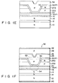
- a P type In 0.5 (Ga 0.5 Al 0.5 ) 0.5 P layer 32 and a P type In 0.5 (Ga 0.3 Al 0.7 ) 0.5 P layer 34 are formed on layers 20, 22a, and 24a in sequence so as to cover the inverse-mesa type groove section 30, as shown in Figure 1E.
- the P type layer 32 acts as an optical waveguide layer for the semiconductor laser
- the P type layer 34 serves as a fourth cladding layer if the layers 14, 18, and 22 are a first, a second, and third cladding layer, respectively.
- a P type InGaP thin-film layer 36 is then formed on the P type layer 34 as shown in Figure 1F.
- a P type GaAs ohmic contact layer 38 is formed on top of this.
- the InGaP thin-film layer 36 has a band-gap value preselected so as to fall between the band-gap values of the upper and lower layers 38 and 34 between which the layer 36 is sandwiched, thereby permitting it to function as an intermediate band-gap layer.
- a metallic layer 40 is formed and, at the same time, on the flat top surface of the ohmic contact layer 38, a metallic layer 42 is formed. These metallic layers 40 and 42 act as electrodes for the semiconductor laser. Now the processes so far described have completed a semiconductor laser 50 with the effective refractive index waveguide structure according to the preferred embodiment of the present invention.
- the inverse-mesa-type groove section 30 is formed in the stacked component consisting of the third cladding layer 22a on which the current-narrowing layer 24a is placed.
- the region into which current required for laser light oscillation in the semiconductor laser 50 is injected is roughly represented in a dotted line 52, while the region in which the oscillation laser light is confined, or the optical waveguide region is indicated by a broken line 54.
- the inverse-mesa-type groove section 30 formed in the P type cladding layer 22a and the N type current-blocking layer 24a causes the width of the optical confinement region 54 to be substantially narrower than that of the current-injection region 52.
- the injection current flow is confined in the region 52 corresponding to the upper opening section of the inverse-mesa-type groove section.
- the emission of light takes place in and around the central region of the active layer 16 immediately below the current injection region 52, resulting in laser oscillation.
- the optical field exuding toward the third cladding layer 22a is effectively confined in the region 54 due to the refractive-index difference at the boundary between the optical waveguide region 54 and the third cladding layer 22a, thereby minimizing the absorption loss of the oscillation light.
- the narrower width of the region 54 than that of the region 52 further increases the optical confinement efficiency, which makes the astigmatism still smaller, thus improving the light-emission efficiency.
- Such a propagation state of oscillation light may be considered to resemble a fundamental transverse-mode oscillation.
- the aforementioned manufacturing method of the semiconductor laser 50 having the inverse-mesa-type groove section is characterized mainly by the use of the etching stopper layer 20 placed between the double-heterostructure section and the third cladding layer 22a thereon. More specifically, in performing the two-stage etching of the inverse-mesa-type groove section 30 into the third cladding layer 22 and current-narrowing layer 24, use of the etching stopper layer 20 with a suitably selected thickness prevents undesirable overetching almost perfectly. This facilitates the high-accuracy control of etching conditions for manufacturing processes such as accurate thickness control of the bottom of the striped groove section 30. This feature will be very helpful to semiconductor manufacturers who are to fabricate semiconductor lasers 50 with an accurately-dimensioned inverse-mesa-type groove section 30.
- etching stopper layer 20 consisting of a completely-aluminum(Al)-free semiconductor layer, or an indium gallium phosphide layer, achieves the layer 32 crystal-grown on the etching stopper with a very high crystallizability, which improves the current-voltage characteristics of the semiconductor laser 50. This not only contributes to the prevention of kink and an improvement in the linearity of the current-light output characteristics, but also allows the expectation of an improvement in the temperature characteristics of the semiconductor laser 50.
- an N type GaAs buffer 102 on an N type GaAs substrate 100 prepared beforehand, an N type GaAs buffer 102, an N type In 0.5 (Ga 0.3 Al 0.7 ) 0.5 P layer 104, a nondoped In 0.5 Ga 0.5 P layer 106, and a P type In 0.5 (Ga 0.3 Al 0.7 ) 0.5 P layer 108 are formed in sequence by using an existing crystal growth technique, such as the MOCVD method.
- the N type layer 104 once the semiconductor laser has been completed, functions as a first cladding layer.
- the layers 106 and 108 act as an active layer and a second cladding layer, respectively. Layers 104, 106, and 108 constitute a double-heterostructure section.
- a P type aluminum-free semiconductive thin film of gallium family such as an InGaP layer 110 is then formed.
- a P type InGaP thin-film layer 110 Formed sequentially on the P type InGaP thin-film layer 110 are a P type In 0.5 (Ga 0.3 Al 0.7 ) 0.5 P layer 112, a P type aluminum-free gallium-family semiconductive thin film such as a P type InGaP layer 114, and an N type GaAs layer 116.
- the layer 116 corresponds to a current-blocking layer.
- a photoresist layer 118 is deposited as shown in Figure 2B.
- the photoresist layer 118 is subjected to a known photopatterning processing, which produces a long, narrow opening 120 in and around the central region of the photoresist layer 118.
- the opening 120 may be called the stripe-shaped opening.
- the N type current-blocking layer 116 immediately below the layer 118a is etched.
- the etchant used here was a mixed solution containing sulfuric acid, hydrogen-peroxide solution, and water at a volume ratio of 3:1:1 (the solution generally known as the "SH etchant"). With such etching processes, what is called “side etching” occurs in the N type GaAs current-blocking layer 116, in which a stripe-shaped opening 122 is formed which is sufficiently wider than the mask opening 120.
- the etching stopper layer 114 sandwiched between the etched layer 116a and the P type In 0.5 (Ga 0.3 Al 0.7 ) 0.5 P layer 112 is etched by using an etchant that are highly corrosive to InGaP and, at the same time, extremely less corrosive to GaAs and InGaAlP, that is, an etchant that allows highly selective etching.
- an etchant for etching the etching stopper layer 114 a solution of hydrogen bromide family is recommendable, for example.
- the P type In 0.5 (Ga 0.3 Al 0.7 ) 0.5 P cladding layer 112 is etched by using hot sulfuric acid, which acts chemically on InGaAlP only.
- the underlying In 0.5 (Ga 0.3 Al 0.7 ) 0.5 P cladding layer 112 is etched so as to define a stripe-shaped opening 126 with an inverse-mesa cross section just below the opening 124.
- the remaining layers 114a, 116a, and 118a retains their shapes as they were first etched into.
- the InGaP thin film 110 that functions as an etching stopper layer lies between the P type cladding layer 112a being etched and the P type In 0.5 (Ga 0.3 Al 0.7 ) 0.5 P cladding layer 108 below the layer 112a, this prevents the underlying layer 108 from being etched unexpectedly.
- the etching process at layer 112a therefore, can progress smoothly without additional limitations until the opening 126 takes the desired cross section.
- stepped inverse-mesa-shaped opening 128 This opening 128 may also be expressed as a stripe-form groove narrower at the bottom and wider at the top.
- a P type In 0.5 (Ga 0.5 Al 0.5 ) 0.5 P layer 130 is formed by crystal growth to entirely cover the exposed surfaces of the stepped inverse-mesa groove section 128.
- the P type layer 130 serves as an optical waveguide layer.
- a P type In 0.5 (Ga 0.3 Al 0.7 ) 0.5 P layer 132 is formed to a predetermined thickness.
- a P type In 0.5 Ga 0.5 P intermediate band-gap layer 134 and a P type GaAs contact layer 136 are formed sequentially on the top surface of the stacked layer component of Figure 2G.
- an AuGe layer 138 and an AuZn layer 140 are formed on the substrate 100 and the P type contact layer 136, respectively, which completes the semiconductor laser 150 according to the second embodiment of the present invention.
- the AuZn layer 138 acts as the P-side electrode in the semiconductor laser 150, while the AuGe layer 138 functions as the N-side electrode.
- the narrower optical confinement region than the exciting-current injected region increases the confinement efficiency of oscillated laser light, allowing the light beam to converge on an extremely small spot with high accuracy.
- the P type In 0.5 (Ga 0.5 Al 0.5 ) 0.5 P optical waveguide layer 130 is partially mounted over the inner top surfaces 152 of the P type InGaP thin-film layer 114a serving as the upper etching stopper layer.
- the optical waveguide layer 130 chemically containing aluminum (Al) can be said to be electrically connected, via the P type etching stopper layer 114a totally free from aluminum, to the P type cladding layer 112a under the stopper layer 114a.
- This arrangement promotes the supply of injected current at the surfaces 152 of the layer 114a, making a great contribution to improving the light emission efficiency of the semiconductor laser 150.
- the semiconductor laser 150 of Figure 2H may be modified as shown in Figure 3, wherein each layer is opposite in the conductivity type to that in the semiconductor laser 150 of Figure 2H. More specifically, this modified semiconductor laser contains a P type GaAs substrate 200, a P type In 0.5 Ga 0.5 P buffer layer 202, a first cladding layer 204 of the P type In 0.5 (Ga 0.3 Al 0.7 ) 0.5 P, a nondoped In 0.5 Ga 0.5 P active layer 206, a second cladding layer 208 of the N type In 0.5 (Ga 0.3 Al 0.7 ) 0.5 P, and an N type InGaP first etching stopper layer 210.
- a third cladding layer 212 of the N type In 0.5 (Ga 0.3 Al 0.7 ) 0.5 P is formed on the layer 210.
- An N type InGaP second etching-stopper layer 214 and a P type GaAs current-blocking layer 216 are formed by the MOCVD method so as to provide the aforementioned stepped inverse-mesa groove structure 128.
- An N type In 0.5 (Ga 0.5 Al 0.5 ) 0.5 P optical waveguide layer 230 is formed so as to cover the stepped inverse-mesa groove structure 128.
- a fourth cladding layer 232 of the N type In 0.5 (Ga 0.3 Al 0.7 ) 0.5 P and an N type GaAs contact layer 236 are formed in sequence.
- an AuZn layer 238 is formed as a P-side electrode, and on the N type contact layer 236, an AuGe layer 240 is produced as an N-side electrode.
- the contact layer 236 especially designed to have the N type conductivity eliminates the intermediate band-gap layer 134 used in the embodiment of Figure 2H. This is because the injection current tends to flow smoothly between the N type InGaAlP layer 232 and the N type GaAs layer 236 even in the absence of such an intermediate band-gap layer.
- multi-etching processes according to the manufacturing method in connection with the present invention in Figures 2A through 2H are not restricted to the inverse-mesa cross-sectional groove section 128 previously described, and may be applied to the manufacture of other types of semiconductor lasers having a stepped cross-sectional structure.
Landscapes
- Physics & Mathematics (AREA)
- Geometry (AREA)
- Condensed Matter Physics & Semiconductors (AREA)
- General Physics & Mathematics (AREA)
- Electromagnetism (AREA)
- Optics & Photonics (AREA)
- Semiconductor Lasers (AREA)
Claims (16)
- Dispositif de laser à semiconducteur comprenant un substrat semiconducteur (10, 100, 200, 302) d'un premier type de conductivité et une section à double hétérostructure prévue au-dessus dudit substrat, dans lequel ladite section à double hétérostructure comporte une première couche de gainage (14, 104, 204) du premier type de conductivité, une couche active (16, 106) prévue sur ladite première couche de gainage et une seconde couche de gainage (18, 108) d'un second type de conductivité prévue dans ladite couche active,
caractérisé en ce que ledit dispositif comprend en outre :une troisième couche de gainage (22a, 112a, 212, 310) prévue au-dessus de ladite seconde couche de gainage (18, 108) ;une couche de blocage de courant (24a, 116a, 216, 318) prévue sur ou au-dessus de ladite troisième couche de gainage, ladite troisième couche de gainage et ladite couche de blocage de courant comportant une section de gorge (30, 128) dans une région présélectionnée ;une couche de guide optique (32, 130) du second type de conductivité prévue sur ladite troisième couche de gainage et ladite couche de blocage de courant de manière à recouvrir ladite section de gorge ; etune quatrième couche de gainage (34, 132, 232) du second type de conductivité prévue sur ladite couche de guide optique, et en ce que ladite section de gorge est agencée en coupe de telle sorte qu'une région de confinement optique (54) dudit dispositif de laser soit d'une largeur inférieure à celle d'une région d'injection de courant (52) afférente. - Dispositif selon la revendication 1, caractérisé en ce que ladite section de gorge (30, 108) présente une section en coupe sensiblement trapézoïdale inverse.
- Dispositif selon la revendication 1, caractérisé en ce que ladite gorge (128) présente une forme de marche en une position correspondant à une interface de jonction entre ladite troisième couche de gainage (112a) et ladite couche de blocage de courant (116a) et globalement, présente une section en coupe quasi-trapézoïdale inverse.
- Dispositif selon la revendication 1 ou 2, caractérisé en ce qu'il comprend en outre une couche en film mince semiconductrice (20, 110) positionnée sur ladite seconde couche de gainage (18, 108) essentiellement chimiquement insensible à une gravure à l'aide d'un agent de gravure spécifique, ladite couche en film mince définissant une surface de fond de ladite section de gorge (30, 108).
- Dispositif selon la revendication 1, 2 ou 3, caractérisé en ce qu'il comprend en outre : une première couche en film mince semiconductrice (110) prévue sur ladite seconde couche de gainage (108), essentiellement chimiquement insensible à une gravure au moyen d'un agent de gravure spécifique, ladite couche en film mince définissant une surface de fond de ladite section de gorge ; et une seconde couche en film mince semiconductrice (114) prise en sandwich entre ladite troisième couche de gainage (112a) et ladite couche de blocage de courant (116a), sensiblement chimiquement insensible à une gravure au moyen d'un agent de gravure spécifié, ladite seconde couche en film mince définissant la forme d'une marche dans ladite section de gorge (128).
- Dispositif selon la revendication 4, caractérisé en ce que lesdites première, seconde et troisième couches de gainage (14, 18, 22a) comprennent un matériau semiconducteur contenant en son sein de l'indium, du gallium, de l'aluminium et du phosphore et en ce que ladite couche en film mince (20) comprend un matériau semiconducteur contenant de l'indium, du gallium et du phosphore, et est exempte d'aluminium.
- Dispositif selon la revendication 5, caractérisé en ce que lesdites première, seconde et troisième couches de gainage (104, 108, 112a) comprennent un matériau semiconducteur contenant en son sein de l'indium, du gallium, de l'aluminium et du phosphore et en ce que lesdites première et seconde couches en film mince (110, 114a) sont réalisées à partir d'un matériau semiconducteur contenant de l'indium, du gallium et du phosphore, et sont exemptes d'aluminium.
- Procédé de fabrication d'un laser à semiconducteur dans lequel une section à double hétérostructure est formée au moyen d'une croissance cristalline au-dessus d'un substrat semiconducteur (10, 100, 200, 302) de manière à comporter une première couche de gainage (14, 104, 204) d'un premier type de conductivité, une couche active (16, 106) formée sur ladite première couche de gainage et une seconde couche de gainage (18, 108) d'un second type de conductivité formée sur ladite couche active, caractérisé en ce que ledit procédé comprend les étapes de : formation sur ladite seconde couche de gainage (18, 108) d'une couche en film mince semiconductrice (20, 110) sensiblement chimiquement insensible à une gravure au moyen d'un agent de gravure spécifié, en tant qu'arrêt de gravure ; formation au moyen d'une croissance cristalline d'une troisième couche de gainage (22a, 112a, 212, 310) du second type de conductivité sur ladite couche d'arrêt de gravure (20, 110) et d'une couche de blocage de courant (24a, 116a, 216, 318) sur ou au-dessus de ladite troisième couche de gainage ; formation d'une section en forme de bande dans ladite troisième couche de gainage et dans ladite couche de blocage de courant en utilisant ledit agent de gravure spécifié de telle sorte que ladite section en forme de bande ait dans sa partie de fond une région de confinement optique qui est d'une largeur plus étroite que celle d'une région d'injection de courant définie au niveau de la partie supérieure de ladite section en forme de bande et de telle sorte qu'elle comprenne également une gorge ; formation au moyen d'une croissance cristalline d'une couche de guide optique (32, 130) sur ladite troisième couche de gainage et sur ladite couche de blocage de courant de manière à recouvrir ladite section en forme de bande ; formation d'une quatrième couche de gainage (34, 132, 232) du second type de conductivité sur ladite couche de guide optique; et formation d'une couche de contact semiconductrice (38, 136) sur ladite quatrième couche de gainage (34, 132, 232).
- Procédé selon la revendication 8, caractérisé en ce que ladite section en forme de bande est formée de manière à présenter une gorge comportant au moins une marche suivant sa section en coupe.
- Procédé selon la revendication 9, caractérisé en ce qu'une couche en film mince semiconductrice supplémentaire (114) qui est essentiellement chimiquement insensible à une gravure au moyen d'un agent de gravure particulier sur ladite troisième couche de gainage (112) est formée en tant que second arrêt de gravure et en ce que ladite couche de blocage de courant (116) est formée sur ledit second arrêt de gravure (114).
- Procédé selon la revendication 10, caractérisé en ce qu'il comprend en outre les étapes de : formation par conformation d'une couche de masque en photoréserve (118a) sur ladite couche de blocage de courant (116) de manière à ce qu'elle présente une certaine ouverture (120) ; gravure de ladite couche de blocage de courant (116) en utilisant ladite couche de masque (118a) afin de former dans ladite couche de blocage de courant une première ouverture (122) qui est plus large que ladite certaine ouverture (120) ; gravure de ladite seconde couche d'arrêt de gravure (114) afin de former dans ladite seconde couche d'arrêt de gravure (114) une seconde ouverture (124) qui est plus étroite que ladite première ouverture ; et gravure de ladite troisième couche de gainage (112) en utilisant la seconde couche d'arrêt de gravure résultante (114a) en tant que masque afin de former dans ladite troisième couche de gainage une troisième ouverture (126) qui est plus étroite que ladite première ouverture et ainsi, ladite gorge comportant au moins une marche est produite.
- Procédé selon la revendication 11, caractérisé en ce que ladite première ouverture (122) est formée au moyen d'effets de gravure latérale de manière à être plus large que ladite certaine ouverture (120).
- Procédé selon la revendication 12, caractérisé en ce que ladite couche de masque (118a) reste sensiblement inchangée lorsqu'une action de gravure est en progression dans ladite couche de blocage de courant (116), dans ladite seconde couche d'arrêt de gravure (114) et dans ladite troisième couche de gainage (112).
- Procédé selon la revendication 13, caractérisé en ce que lesdites première, seconde et troisième couches de gainage (14, 18, 22a ; 104, 108, 112a) comprennent un matériau semiconducteur contenant de l'indium, du gallium, de l'aluminium et du phosphore et en ce que lesdites couches d'arrêt de gravure (20, 110, 114) comprennent un matériau semiconducteur contenant de l'indium, du gallium et du phosphore et sont exemptes d'aluminium.
- Procédé selon la revendication 14, caractérisé en ce qu'une solution de mélange contenant de l'acide sulfurique et une solution de péroxyde d'hydrogène est utilisée en tant que dit agent de gravure particulier.
- Procédé selon la revendication 15, caractérisé en ce qu'une solution chimique qui est constituée essentiellement par de l'acide sulfurique chaud est utilisée en tant que dit agent de gravure spécifié.
Applications Claiming Priority (6)
| Application Number | Priority Date | Filing Date | Title |
|---|---|---|---|
| JP4596490A JPH03250685A (ja) | 1990-02-28 | 1990-02-28 | 半導体レーザ装置の製造方法 |
| JP45964/90 | 1990-02-28 | ||
| JP84668/90 | 1990-03-30 | ||
| JP8466890A JP2914711B2 (ja) | 1990-03-30 | 1990-03-30 | 半導体レーザの製造方法 |
| JP84669/90 | 1990-03-30 | ||
| JP8466990A JP2909133B2 (ja) | 1990-03-30 | 1990-03-30 | 半導体レーザ装置 |
Publications (3)
| Publication Number | Publication Date |
|---|---|
| EP0444366A2 EP0444366A2 (fr) | 1991-09-04 |
| EP0444366A3 EP0444366A3 (en) | 1992-01-22 |
| EP0444366B1 true EP0444366B1 (fr) | 1997-02-12 |
Family
ID=27292457
Family Applications (1)
| Application Number | Title | Priority Date | Filing Date |
|---|---|---|---|
| EP90314466A Expired - Lifetime EP0444366B1 (fr) | 1990-02-28 | 1990-12-31 | Laser à semi-conducteur avec une section à rainure de forme mésa inverse |
Country Status (3)
| Country | Link |
|---|---|
| US (1) | US5058120A (fr) |
| EP (1) | EP0444366B1 (fr) |
| DE (1) | DE69029935T2 (fr) |
Families Citing this family (17)
| Publication number | Priority date | Publication date | Assignee | Title |
|---|---|---|---|---|
| EP0456485B1 (fr) * | 1990-05-09 | 1996-07-17 | Sharp Kabushiki Kaisha | Méthode de production d'un composant à semi-conducteur |
| US5144633A (en) * | 1990-05-24 | 1992-09-01 | Matsushita Electric Industrial Co., Ltd. | Semiconductor laser and manufacturing method thereof |
| US5268328A (en) * | 1990-09-07 | 1993-12-07 | Matsushita Electric Industrial Co., Ltd. | Method of fabricating a semiconductor laser |
| JPH04116993A (ja) * | 1990-09-07 | 1992-04-17 | Matsushita Electric Ind Co Ltd | 半導体レーザ及びその製造方法 |
| US5212704A (en) * | 1991-11-27 | 1993-05-18 | At&T Bell Laboratories | Article comprising a strained layer quantum well laser |
| DE69312799T2 (de) * | 1992-05-18 | 1998-02-12 | Philips Electronics Nv | Optoelektronische Halbleiteranordnung |
| JP2914833B2 (ja) * | 1992-09-14 | 1999-07-05 | シャープ株式会社 | 半導体レーザ |
| JPH06296060A (ja) * | 1993-04-08 | 1994-10-21 | Mitsubishi Electric Corp | 半導体可視光レーザダイオードの製造方法 |
| SE506651C2 (sv) * | 1996-02-27 | 1998-01-26 | Ericsson Telefon Ab L M | Begravd heterostruktur |
| US5727012A (en) | 1996-03-07 | 1998-03-10 | Lucent Technologies Inc. | Heterostructure laser |
| US6400743B1 (en) * | 1999-08-05 | 2002-06-04 | Fuji Photo Film Co., Ltd. | High-power semiconductor laser device having current confinement structure and index-guided structure |
| US6589805B2 (en) * | 2001-03-26 | 2003-07-08 | Gazillion Bits, Inc. | Current confinement structure for vertical cavity surface emitting laser |
| US20050141578A1 (en) * | 2003-06-20 | 2005-06-30 | Benoit Reid | Laser diode structure with blocking layer |
| KR100584333B1 (ko) * | 2004-01-08 | 2006-05-26 | 삼성전자주식회사 | 반도체 레이저 장치 및 그 제조방법 |
| CN102037575B (zh) * | 2008-03-27 | 2013-04-10 | 宋俊午 | 发光元件及其制造方法 |
| JP7166871B2 (ja) * | 2018-10-18 | 2022-11-08 | スタンレー電気株式会社 | 垂直共振器型発光素子 |
| JP7190865B2 (ja) | 2018-10-18 | 2022-12-16 | スタンレー電気株式会社 | 垂直共振器型発光素子 |
Citations (1)
| Publication number | Priority date | Publication date | Assignee | Title |
|---|---|---|---|---|
| EP0328134A2 (fr) * | 1988-02-10 | 1989-08-16 | Kabushiki Kaisha Toshiba | Dispositif laser à semi-conducteur et méthode pour la fabrication du dispositif laser à semi-conducteur |
Family Cites Families (7)
| Publication number | Priority date | Publication date | Assignee | Title |
|---|---|---|---|---|
| JPS60110188A (ja) * | 1983-11-18 | 1985-06-15 | Sharp Corp | 半導体レ−ザ素子 |
| JPS60192380A (ja) * | 1984-03-13 | 1985-09-30 | Mitsubishi Electric Corp | 半導体レ−ザ装置 |
| US4799228A (en) * | 1985-08-23 | 1989-01-17 | Kabushiki Kaisha Toshiba | Transverse-mode stabilized semiconductor laser diode with slab-coupled waveguide |
| US4792958A (en) * | 1986-02-28 | 1988-12-20 | Kabushiki Kaisha Toshiba | Semiconductor laser with mesa stripe waveguide structure |
| JP2585230B2 (ja) * | 1986-09-16 | 1997-02-26 | 株式会社日立製作所 | 半導体レ−ザ装置 |
| JP2553580B2 (ja) * | 1987-08-19 | 1996-11-13 | 三菱電機株式会社 | 半導体レ−ザ装置 |
| JPH069282B2 (ja) * | 1988-09-09 | 1994-02-02 | 株式会社東芝 | 半導体レーザ装置 |
-
1990
- 1990-12-27 US US07/634,546 patent/US5058120A/en not_active Expired - Lifetime
- 1990-12-31 DE DE69029935T patent/DE69029935T2/de not_active Expired - Fee Related
- 1990-12-31 EP EP90314466A patent/EP0444366B1/fr not_active Expired - Lifetime
Patent Citations (1)
| Publication number | Priority date | Publication date | Assignee | Title |
|---|---|---|---|---|
| EP0328134A2 (fr) * | 1988-02-10 | 1989-08-16 | Kabushiki Kaisha Toshiba | Dispositif laser à semi-conducteur et méthode pour la fabrication du dispositif laser à semi-conducteur |
Non-Patent Citations (1)
| Title |
|---|
| 18 May 1985 & JP- A-60 003 181 * |
Also Published As
| Publication number | Publication date |
|---|---|
| US5058120A (en) | 1991-10-15 |
| EP0444366A3 (en) | 1992-01-22 |
| DE69029935T2 (de) | 1997-09-04 |
| EP0444366A2 (fr) | 1991-09-04 |
| DE69029935D1 (de) | 1997-03-27 |
Similar Documents
| Publication | Publication Date | Title |
|---|---|---|
| EP0444366B1 (fr) | Laser à semi-conducteur avec une section à rainure de forme mésa inverse | |
| US5143863A (en) | Method of manufacturing semiconductor laser | |
| EP0572917B1 (fr) | Dispositif en semi-conducteur composé et méthode de fabrication du dispositif | |
| US5065402A (en) | Transverse-mode stabilized laser diode | |
| US5602866A (en) | Semiconductor laser | |
| US4757509A (en) | Semiconductor laser apparatus | |
| JP2001274510A (ja) | 導波路型光素子及びその製造方法 | |
| JPH0248151B2 (fr) | ||
| JP2842465B2 (ja) | 半導体レーザ装置およびその製造方法 | |
| JPH09191150A (ja) | 半導体レーザ装置とその製造方法 | |
| JP4014375B2 (ja) | 半導体レーザーの素子構造および製造方法 | |
| JP2973215B2 (ja) | 半導体レーザ装置 | |
| JPS641952B2 (fr) | ||
| JP2946781B2 (ja) | 半導体レーザ | |
| JP2523648B2 (ja) | 半導体レ―ザの製造方法 | |
| JP2833962B2 (ja) | 半導体レーザおよびその製法 | |
| JP3277711B2 (ja) | 半導体レーザ及びその製造方法 | |
| JP2794743B2 (ja) | 量子井戸型半導体レーザ素子 | |
| JP4024319B2 (ja) | 半導体発光装置 | |
| JP2564343B2 (ja) | 半導体レーザ装置 | |
| JPH0671122B2 (ja) | 半導体レーザ素子 | |
| JP3191359B2 (ja) | 半導体レーザー | |
| JPH0446477B2 (fr) | ||
| JPH0569318B2 (fr) | ||
| JPH04229682A (ja) | 半導体レーザの製造方法 |
Legal Events
| Date | Code | Title | Description |
|---|---|---|---|
| PUAI | Public reference made under article 153(3) epc to a published international application that has entered the european phase |
Free format text: ORIGINAL CODE: 0009012 |
|
| 17P | Request for examination filed |
Effective date: 19910102 |
|
| AK | Designated contracting states |
Kind code of ref document: A2 Designated state(s): DE FR GB |
|
| PUAL | Search report despatched |
Free format text: ORIGINAL CODE: 0009013 |
|
| AK | Designated contracting states |
Kind code of ref document: A3 Designated state(s): DE FR GB |
|
| 17Q | First examination report despatched |
Effective date: 19921029 |
|
| GRAG | Despatch of communication of intention to grant |
Free format text: ORIGINAL CODE: EPIDOS AGRA |
|
| GRAH | Despatch of communication of intention to grant a patent |
Free format text: ORIGINAL CODE: EPIDOS IGRA |
|
| GRAH | Despatch of communication of intention to grant a patent |
Free format text: ORIGINAL CODE: EPIDOS IGRA |
|
| RBV | Designated contracting states (corrected) |
Designated state(s): DE FR |
|
| GRAA | (expected) grant |
Free format text: ORIGINAL CODE: 0009210 |
|
| AK | Designated contracting states |
Kind code of ref document: B1 Designated state(s): DE FR |
|
| REF | Corresponds to: |
Ref document number: 69029935 Country of ref document: DE Date of ref document: 19970327 |
|
| ET | Fr: translation filed | ||
| PLBE | No opposition filed within time limit |
Free format text: ORIGINAL CODE: 0009261 |
|
| STAA | Information on the status of an ep patent application or granted ep patent |
Free format text: STATUS: NO OPPOSITION FILED WITHIN TIME LIMIT |
|
| 26N | No opposition filed | ||
| REG | Reference to a national code |
Ref country code: FR Ref legal event code: D6 |
|
| PGFP | Annual fee paid to national office [announced via postgrant information from national office to epo] |
Ref country code: FR Payment date: 20021210 Year of fee payment: 13 |
|
| PGFP | Annual fee paid to national office [announced via postgrant information from national office to epo] |
Ref country code: DE Payment date: 20030109 Year of fee payment: 13 |
|
| PG25 | Lapsed in a contracting state [announced via postgrant information from national office to epo] |
Ref country code: DE Free format text: LAPSE BECAUSE OF NON-PAYMENT OF DUE FEES Effective date: 20040701 |
|
| PG25 | Lapsed in a contracting state [announced via postgrant information from national office to epo] |
Ref country code: FR Free format text: LAPSE BECAUSE OF NON-PAYMENT OF DUE FEES Effective date: 20040831 |
|
| REG | Reference to a national code |
Ref country code: FR Ref legal event code: ST |