EP0444569B1 - Vorrichtung zum Schutz gegen durch An- und Ausschaltung einer elektronischen Einheit an eine Gleichspannungsspeisung erzeugte Speisespannungsstörungen - Google Patents
Vorrichtung zum Schutz gegen durch An- und Ausschaltung einer elektronischen Einheit an eine Gleichspannungsspeisung erzeugte Speisespannungsstörungen Download PDFInfo
- Publication number
- EP0444569B1 EP0444569B1 EP91102722A EP91102722A EP0444569B1 EP 0444569 B1 EP0444569 B1 EP 0444569B1 EP 91102722 A EP91102722 A EP 91102722A EP 91102722 A EP91102722 A EP 91102722A EP 0444569 B1 EP0444569 B1 EP 0444569B1
- Authority
- EP
- European Patent Office
- Prior art keywords
- value
- electronic system
- source
- capacitor
- disconnected
- Prior art date
- Legal status (The legal status is an assumption and is not a legal conclusion. Google has not performed a legal analysis and makes no representation as to the accuracy of the status listed.)
- Revoked
Links
- 239000003990 capacitor Substances 0.000 claims description 25
- 230000005669 field effect Effects 0.000 claims description 4
- 238000007599 discharging Methods 0.000 claims 2
- 230000000712 assembly Effects 0.000 description 6
- 238000000429 assembly Methods 0.000 description 6
- 230000010354 integration Effects 0.000 description 6
- 238000001914 filtration Methods 0.000 description 5
- 230000007423 decrease Effects 0.000 description 3
- 230000005540 biological transmission Effects 0.000 description 2
- 238000010586 diagram Methods 0.000 description 2
- 229920006395 saturated elastomer Polymers 0.000 description 2
- 230000000903 blocking effect Effects 0.000 description 1
- 230000037431 insertion Effects 0.000 description 1
- 238000003780 insertion Methods 0.000 description 1
Images

Classifications
-
- H—ELECTRICITY
- H04—ELECTRIC COMMUNICATION TECHNIQUE
- H04B—TRANSMISSION
- H04B15/00—Suppression or limitation of noise or interference
- H04B15/02—Reducing interference from electric apparatus by means located at or near the interfering apparatus
-
- H—ELECTRICITY
- H02—GENERATION; CONVERSION OR DISTRIBUTION OF ELECTRIC POWER
- H02H—EMERGENCY PROTECTIVE CIRCUIT ARRANGEMENTS
- H02H9/00—Emergency protective circuit arrangements for limiting excess current or voltage without disconnection
- H02H9/001—Emergency protective circuit arrangements for limiting excess current or voltage without disconnection limiting speed of change of electric quantities, e.g. soft switching on or off
- H02H9/004—Emergency protective circuit arrangements for limiting excess current or voltage without disconnection limiting speed of change of electric quantities, e.g. soft switching on or off in connection with live-insertion of plug-in units
-
- Y—GENERAL TAGGING OF NEW TECHNOLOGICAL DEVELOPMENTS; GENERAL TAGGING OF CROSS-SECTIONAL TECHNOLOGIES SPANNING OVER SEVERAL SECTIONS OF THE IPC; TECHNICAL SUBJECTS COVERED BY FORMER USPC CROSS-REFERENCE ART COLLECTIONS [XRACs] AND DIGESTS
- Y10—TECHNICAL SUBJECTS COVERED BY FORMER USPC
- Y10S—TECHNICAL SUBJECTS COVERED BY FORMER USPC CROSS-REFERENCE ART COLLECTIONS [XRACs] AND DIGESTS
- Y10S323/00—Electricity: power supply or regulation systems
- Y10S323/908—Inrush current limiters
Definitions
- the present invention relates to a device for protection against disturbances generated by the connection to a source of continuous electrical power or the disconnection of this source from an electronic assembly, on the power supplied by this source.
- Complex electronic equipment such as telecommunications equipment generally consists of electronic assemblies such as printed circuit boards fitted with electronic components, plugged into trays, or chassis, themselves grouped in racks or cabinets.
- the power supply necessary for the operation of the electronic components carried by these cards is generally delivered by a DC voltage source common to the different cards of the same frame.
- each card in the access circuit of the supply voltage of this card, one or more filter cells capable of preventing the transmission to the electronic circuits of this card of any electrical interference present. on the supply voltage and vice versa the transmission to the DC supply voltage source of any electrical interference generated by this card in operation.
- FIG. 1 An example of such a filter cell is shown in Figure 1; it is an LC type cell, comprising an inductor L1 and a capacitor C2, the DC supply voltage V being applied across the L1-C2 assembly, and the output voltage being taken across the capacitor C2.
- the filtering function of this cell is all the better fulfilled the higher the values of the inductance L1 and of the capacitor C2.
- the values of these elements are however optimized to take into account other criteria such as size and cost.
- the capacitor C2 charges very quickly through the inductor L1, which results in a large current draw on the power source.
- this source generally consisting of a DC-DC converter (for example a 48V / 5V converter in the case of telecommunications equipment) is equipped with a voltage control loop
- this control is generally slow to occur before the charging time of the capacitor C2 and there is a momentary drop in the supply voltage during this charging time, which may disturb the operation of certain circuits in operation at this time on other cards.
- Another solution would be to decrease the value of the capacitor C2 or to have a resistor in series with this capacitor, hence a greater impedance presented by this element and a current draw by the card considered, on the power source, weaker when connecting this card.
- the object of the present invention is to avoid these drawbacks, that is to say to avoid the generation of the disturbances described, on the supply delivered by the common source of supply of the cards, at the time of connection or disconnection of cards, while maintaining the efficiency of the filtering cells of these cards.
- the subject of the present invention is a device for protection against disturbances generated by the connection to a source of continuous electrical power or the disconnection of this source from an electronic assembly, on the electrical power supplied by this source, said device being essentially characterized in that it comprises at least one variable impedance element, and means for controlling this impedance, so that it has a very large first value when said electronic assembly is in the disconnected state, a second value very low when this set is in the connected state, and a value varying slowly from the first to the second value on passing from the disconnected state to the connected state, and rapidly varying from the second to the first value at the passage from the connected state to the disconnected state, the current obtained at the output of this element supplying said electro assembly fuck.
- the protection device according to the invention represented in FIG. 2 where it is marked with 1, is placed between terminals 20 and 30 connected respectively to the supply ports 2 and 3 of an electronic assembly which it equips, and the filter cell 4 fitted to this assembly.
- the electronic assembly considered is for example a printed circuit board pluggable into a chassis or tray of an electronic equipment frame having a continuous power source common to the different cards of the different chassis.
- a connector 6 said card connector, and a connector 7, said chassis connector , or tray, containing the card considered these two connectors making it possible to establish electrical continuity between the card and its supply ports 2, 3, when the card is connected, or to break this continuity when the card is disconnected.
- a load 5 representing the circuits of the card considered, other than the protection device 1 and the filter cell 4.
- a supply voltage of a single polarity positive for example (denoted + V) is used, this voltage being applied to one of the supply ports, the port 2 for example, the other access being set to the reference potential 0 volts.
- the protection device 1 comprises, in the embodiment described, an integration cell formed by a capacitor C1 and a resistor R1 connected in series in this order between the terminals 20 and 30, and a field effect power transistor T1 constituted in this case by a P channel MOS type transistor.
- the input voltage of this cell constituted by the voltage across capacitor C1 and resistor R1 in series is equal to + V when the card is connected or to 0 volts when the card is disconnected.
- the output voltage of this integration cell, taken across the capacitor C1 constitutes the source-gate voltage VSG, of the transistor T1, the source of which is connected to terminal 20 and the gate at the point common to the capacitor C1 and to resistance R1.
- the drain current ID delivered by the transistor T1 supplies the filter cell L1-C2.
- a diode D1 is also arranged between the point common to the capacitor C1 and to the resistor R1, and the terminal 30.
- this protection device is as follows. When the card fitted with this protection device is connected, the input voltage of the integration cell R1-C1 suddenly goes from 0 to + V. The output voltage of this integration cell, that is to say the source-gate voltage VSG of the transistor T1, then increases slowly from 0 to + V. From a certain value of the voltage VSG, the-transistor T1, initially blocked, becomes conductive.
- the apparent drain-source resistance of the transistor T1 initially very large (> 1 M ⁇ for example), then gradually decreases and the capacitor C2 therefore gradually charges with a current limited by the value of this resistance.
- the transistor T1 When the capacitor C1 is fully charged, the transistor T1 is saturated, its apparent drain-source resistance is then very low (of the order of 100 m ⁇ for example) and the protection device is then "transparent".
- the time during which the charging current of the capacitor C2 is thus controlled must be much greater (of the order of 20 ms for example) than the charging time of the capacitor C2 in the absence of this protection device (of the order of 200 ⁇ s for example), so as to allow the servo loop of the DC-DC converter to fulfill its role, that is to say here d '' avoid a temporary drop in the supply voltage + V.
- the components R1, C1 and T1 are determined accordingly.
- Apparent resistance drain-source of transistor T1 in the saturated state is moreover determined as a function of the current necessary to supply the card when the latter is operating in steady state.
- the capacitor C1 When the card is disconnected, the capacitor C1 is initially charged at voltage + V and the potential applied to one of its terminals, connected to terminal 20, i.e. to access 2 through the connectors 6 and 7, suddenly varying from + V to 0, the potential at its other terminal, connected to the cathode of diode D1 (the anode of diode D1 being connected to access 3 by connectors 6 and 7) suddenly becomes negative with respect to the 0 volt potential.
- the diode D1 initially blocked then becomes on.
- the capacitor C1 therefore discharges very quickly through this diode while the source-gate voltage VSG of the transistor T1 decreases very quickly resulting in the blocking of the transistor T1.
- This blockage which occurs very quickly (in practice in a few nanoseconds), prevents any disturbance on the drain side, due in particular to the presence of the filter cell L1-C2, from being transmitted on the source side of the transistor T1, that is to say say from the DC supply side.
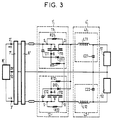
- the embodiment of the protection device according to the invention shown in FIG. 3 corresponds to the case of a supply of the card with a positive voltage + V and a negative voltage -V, applied respectively to the supply ports marked 2 ′ And 3 ′, the reference potential 0V being placed on an access marked 10.
- the power source supplying the two voltages + V and -V and to which the accesses 2 ′, 3 ′ and 10 are connected is referenced 8 ′ and the protection device itself is referenced 1 ′.
- the filter cell identified 4 ′, then breaks down in known manner into two filter cells 41 and 42 of these two voltages.
- These two cells are here each analogous to cell 4 in FIG. 2 and therefore each comprise an inductor and a capacitor, respectively L11 and C21 and L12 and C22.
- At the output of these two cells 41 and 42 are disposed respectively two loads 51 and 52 representing the circuits of the considered card supplied through the protection device 1 ′ and respectively cells 41 and 42.
- the protection device 1 ′ connected to the supply accesses 2 ′, 3 ′ and 10 by a card connector 6 ′ and a chassis or tray connector 7 ′, is also broken down into two devices 11 and 12 each comprising, as the protection device 1 of FIG. 2, a field effect power transistor T11, an integration cell R11, C11 and a diode D11 for the first, a field effect power transistor T12, a cell integration R12, C12 and a diode D12 for the second, with however the following differences.
- the transistor T11 of the device 11 is like the transistor T1 of the device 1 of FIG. 2 a MOS type transistor with P channel, its source being connected through the connectors 6 ′ and 7 ′ to the power supply access 2 ′ at the positive potential + V (and its drain at the input terminal of the filtering cell 41 connected to the inductance L11), the transistor T12 of the device 12 is an N-channel MOS type transistor, its source being connected to through the connectors 6 ′ and 7 ′ to the supply access 3 ′ at the negative potential -V (and its drain at the input terminal of the filter cell 42 connected to the inductance L12).
- a resistor R21 is also connected between the source S and the drain D of the transistor T11, likewise a resistor R22 is connected between the source S and the drain D of the transistor T12.
- the resistors R21 and R22 In order not to reduce the performance of the assembly, the resistors R21 and R22 must have a high value, for example of the order of 1M ⁇ .
- the invention has been described in the context of an application to a printed circuit board which can be plugged into a chassis of a rack of electronic equipment, but it is obvious that it is not limited to this application. It can be applied in particular to each electronic assembly of a group of electronic assemblies supplied by a common continuous electrical power source and individually connectable and disconnectable from this source, to avoid generation, at the time of connection or the electrical disconnection of one of these assemblies, of disturbances on the supply delivered by this common source and consequently on the supply of those of the other assemblies of the group which are at this time connected to the source.
- the protection device according to the invention particularly effective in the case of the use of individual filtering cells of the power supply at the level of these different electronic assemblies, nevertheless retains its usefulness in the absence of such cells.
- individual filtering in particular to avoid a possible drop in the supply voltage supplied by the common power source of these assemblies when one of them is connected.
Landscapes
- Engineering & Computer Science (AREA)
- Computer Networks & Wireless Communication (AREA)
- Signal Processing (AREA)
- Direct Current Feeding And Distribution (AREA)
- Emergency Protection Circuit Devices (AREA)
- Optical Communication System (AREA)
- Amplifiers (AREA)
- Details Of Television Scanning (AREA)
- Details Of Connecting Devices For Male And Female Coupling (AREA)
- Dc-Dc Converters (AREA)
- Control Or Security For Electrophotography (AREA)
Claims (6)
- Vorrichtung zum Schutz gegen Störungen, die durch das Anschließen einer elektronischen Einheit an eine elektrische Gleichspannungsversorgungsquelle oder das Abtrennen von dieser Quelle auf die von dieser Quelle gelieferte elektrische Spannung verursacht werden, dadurch gekennzeichnet, daß die Vorrichtung mindestens ein veränderliches Impedanzelement (T1) und Mittel (R1, C1, D1) zum Steuern dieser Impedanz aufweist, derart, daß diese einen ersten sehr großen Wert besitzt, wenn die elektronische Einheit abgeschaltet ist, und einen sehr kleinen Wert besitzt, wenn die Einheit angeschaltet ist, und beim Übergang vom abgeschalteten Zustand in den angeschalteten Zustand langsam vom ersten in den zweiten Wert übergeht und sich beim Übergang vom angeschalteten Zustand in den abgeschalteten Zustand schnell vom zweiten in den ersten Wert übergeht, wobei der am Ausgang dieses Elementes erhaltene Strom die elektronische Einheit speist.
- Vorrichtung nach Anspruch 1, dadurch gekennzeichnet, daß das veränderliche Impedanzelement einen Feldeffekt-Leistungstransistor (T1) aufweist, dessen Source-Gate-Spannung von den Steuermitteln (R1, C1, D1) dieses Elementes geliefert wird und dessen Drain-Strom den Speisestrom der elektronischen Einheit bildet.
- Vorrichtung nach Anspruch 1, dadurch gekennzeichnet, daß die Steuermittel eine Integrierzelle des Typs R-C (R1, C1), die von der Speisespannung gespeist wird, die die Quelle liefert, wenn die elektronische Einheit angeschaltet ist, und die nicht gespeist wird, wenn die Einheit abgeschaltet ist, und eine Diode (D1) zum Entladen des Kondensators (C1) der Integrierzelle beim Übergang der elektronischen Einheit vom angeschalteten Zustand in den abgeschalteten Zustand aufweist.
- Vorrichtung nach einem der Ansprüche 1 bis 3, dadurch gekennzeichnet, daß die Versorgungsspannung zwei entgegengesetzt gepolte Vorspannungen an die elektronische Einheit liefert und für jede dieser Vorspannungen die Elemente gemäß einem der obigen Ansprüche aufweist.
- Vorrichtung nach den Ansprüchen 3 und 4, dadurch gekennzeichnet, daß für jede der Vorspannungen die Entladungsdiode (D11, D12) des Kondensators (C11, C12) der dieser Vorspannung zugeordneten Integrierzelle einerseits an eine der Klemmen des Kondensators und andererseits an den Ausgang des veränderlichen Impedanzelementes (T12, T11) angeschlossen ist, das der anderen Vorspannung zugeordnet ist.
- Vorrichtung nach den Ansprüchen 3 und 4, dadurch gekennzeichnet, daß die jeder Vorspannung zugeordnete Integrierzelle des Typs R-C weiter einen Widerstand (R21; R22) mit einem sehr hohen Wert aufweist, der parallel an das der anderen Vorspannung zugeordnete Element veränderlicher Impedanz (T11, T12) angeschlossen ist.
Applications Claiming Priority (2)
| Application Number | Priority Date | Filing Date | Title |
|---|---|---|---|
| FR9002511A FR2658968B1 (fr) | 1990-02-28 | 1990-02-28 | Dispositif de protection contre les perturbations engendrees par la connexion a une source d'alimentation electrique continue ou la deconnexion de cette source d'un ensemble electronique, sur l'alimentation delivree par cette source. |
| FR9002511 | 1990-02-28 |
Publications (2)
| Publication Number | Publication Date |
|---|---|
| EP0444569A1 EP0444569A1 (de) | 1991-09-04 |
| EP0444569B1 true EP0444569B1 (de) | 1994-12-07 |
Family
ID=9394233
Family Applications (1)
| Application Number | Title | Priority Date | Filing Date |
|---|---|---|---|
| EP91102722A Revoked EP0444569B1 (de) | 1990-02-28 | 1991-02-25 | Vorrichtung zum Schutz gegen durch An- und Ausschaltung einer elektronischen Einheit an eine Gleichspannungsspeisung erzeugte Speisespannungsstörungen |
Country Status (9)
| Country | Link |
|---|---|
| US (1) | US5155648A (de) |
| EP (1) | EP0444569B1 (de) |
| JP (1) | JP3061202B2 (de) |
| AT (1) | ATE115338T1 (de) |
| AU (1) | AU639756B2 (de) |
| CA (1) | CA2037125A1 (de) |
| DE (1) | DE69105548T2 (de) |
| ES (1) | ES2065561T3 (de) |
| FR (1) | FR2658968B1 (de) |
Families Citing this family (29)
| Publication number | Priority date | Publication date | Assignee | Title |
|---|---|---|---|---|
| US5283707A (en) * | 1992-11-27 | 1994-02-01 | Northern Telecom Limited | Inrush current limiting circuit |
| JP3470809B2 (ja) * | 1992-12-02 | 2003-11-25 | イーエムシー コーポレイション | インラッシュ電流リミッター |
| DE69425884T2 (de) * | 1994-07-29 | 2001-03-08 | Alcatel Bell N.V., Antwerpen | Stromsteuerungsschnitstellenschaltung |
| US6046896A (en) | 1995-08-11 | 2000-04-04 | Fijitsu Limited | DC-to-DC converter capable of preventing overvoltage |
| US5714809A (en) * | 1995-10-12 | 1998-02-03 | International Business Machines Corporation | Soft switching circuit with current-mode control |
| US6188305B1 (en) | 1995-12-08 | 2001-02-13 | International Business Machines Corporation | Transformer formed in conjunction with printed circuit board |
| US5737165A (en) * | 1996-02-08 | 1998-04-07 | Ilc Data Device Corporation | Apparatus for databus fault isolation |
| US5774315A (en) * | 1996-08-19 | 1998-06-30 | Core Engineering, Inc. | Power surge suppression circuit for hot plug environments |
| US5990723A (en) * | 1998-01-09 | 1999-11-23 | Maxim Integrated Products, Inc. | Filter circuits for protecting against transient electrical pulses |
| DE19847014A1 (de) | 1998-10-13 | 2000-04-20 | Bosch Gmbh Robert | Filtervorrichtung zum Ausfiltern von Versorgungsspannungsstörungen |
| US6335654B1 (en) | 2000-03-17 | 2002-01-01 | The United States Of America As Represented By The Administrator Of The National Aeronautics And Space Administration | Inrush current control circuit |
| JP2001313127A (ja) * | 2000-04-28 | 2001-11-09 | Nec Corp | 電子機器における静電気破壊防止装置 |
| WO2002067279A2 (en) * | 2000-12-22 | 2002-08-29 | Ixys Corporation | Hot-swap protection circuit |
| US7405495B2 (en) * | 2002-01-22 | 2008-07-29 | Johnson Controls Automotive Electronics | Multicellular DC/DC voltage converter with protection switches |
| US6703889B2 (en) | 2002-02-14 | 2004-03-09 | Adc Dsl Systems, Inc. | In-rush current protection |
| US6807039B2 (en) * | 2002-07-08 | 2004-10-19 | Adc Dsl Systems, Inc. | Inrush limiter circuit |
| US20040169981A1 (en) * | 2002-09-19 | 2004-09-02 | Andy Werback | Current limiting circuit |
| US20040070908A1 (en) * | 2002-09-27 | 2004-04-15 | International Business Machines Corporation | Overcurrent protection of input/output devices in a data processing system |
| HUP0400421A2 (hu) * | 2004-02-16 | 2005-12-28 | András Fazakas | Kapcsolási elrendezés egy legalább 500 mikroFarad kapacitású elektrolitikus kondenzátornak egy energiát tároló másik elektrolitikus kondenzátorral való vezérelt párhuzamos kapcsolására |
| TWI339481B (en) * | 2007-01-29 | 2011-03-21 | Chimei Innolux Corp | Power supplying and discharging circuit |
| US7741821B2 (en) * | 2007-09-18 | 2010-06-22 | International Business Machines Corporation | Start-up circuit and method for high voltage power distribution circuit |
| JP2010172092A (ja) * | 2009-01-21 | 2010-08-05 | Funai Electric Co Ltd | 同期整流回路 |
| CN102196071B (zh) * | 2010-07-30 | 2013-02-20 | 惠州Tcl移动通信有限公司 | 一种移动终端 |
| CN103081270B (zh) * | 2010-08-31 | 2015-07-29 | 伊顿公司 | 高压直流系统中控制直流电弧的高压电子开关及其操作方法 |
| US8717717B2 (en) * | 2011-08-04 | 2014-05-06 | Futurewei Technologies, Inc. | High efficiency power regulator and method |
| JP6291432B2 (ja) * | 2015-02-04 | 2018-03-14 | 矢崎総業株式会社 | 突入電流抑制回路 |
| CN105098703A (zh) * | 2015-09-25 | 2015-11-25 | 上海斐讯数据通信技术有限公司 | 一种测试系统 |
| CN106787867B (zh) * | 2016-11-30 | 2019-09-06 | 上海航天控制技术研究所 | 一种速率陀螺仪供电电源 |
| US11424614B2 (en) * | 2019-09-25 | 2022-08-23 | Landis+Gyr Innovations, Inc. | System for limiting inrush current in a battery endpoint |
Family Cites Families (6)
| Publication number | Priority date | Publication date | Assignee | Title |
|---|---|---|---|---|
| US3912974A (en) * | 1970-02-18 | 1975-10-14 | George Leslie Hill | Circuit breaker |
| US3968421A (en) * | 1974-12-30 | 1976-07-06 | Whirlpool Corporation | Delayed on quick off regulator circuit for appliance control |
| US4658320A (en) * | 1985-03-08 | 1987-04-14 | Elecspec Corporation | Switch contact arc suppressor |
| US4891728A (en) * | 1986-12-23 | 1990-01-02 | Siemens Aktiengesellschaft | Circuit arrangement for limiting the switch-on current and for providing an over voltage protection in switch mode power supply devices |
| FR2615669B1 (fr) * | 1987-05-19 | 1996-07-05 | Cit Alcatel | Dispositif de limitation des perturbations electriques a l'enfichage et au defichage d'une carte electronique |
| US4814687A (en) * | 1988-01-21 | 1989-03-21 | Honeywell, Inc. | Following voltage/current regulator |
-
1990
- 1990-02-28 FR FR9002511A patent/FR2658968B1/fr not_active Expired - Lifetime
-
1991
- 1991-02-25 DE DE69105548T patent/DE69105548T2/de not_active Revoked
- 1991-02-25 ES ES91102722T patent/ES2065561T3/es not_active Expired - Lifetime
- 1991-02-25 AT AT91102722T patent/ATE115338T1/de not_active IP Right Cessation
- 1991-02-25 EP EP91102722A patent/EP0444569B1/de not_active Revoked
- 1991-02-26 CA CA002037125A patent/CA2037125A1/fr not_active Abandoned
- 1991-02-27 AU AU71978/91A patent/AU639756B2/en not_active Ceased
- 1991-02-27 JP JP3056184A patent/JP3061202B2/ja not_active Expired - Lifetime
- 1991-02-27 US US07/661,147 patent/US5155648A/en not_active Expired - Fee Related
Also Published As
| Publication number | Publication date |
|---|---|
| FR2658968B1 (fr) | 1992-05-07 |
| FR2658968A1 (fr) | 1991-08-30 |
| DE69105548D1 (de) | 1995-01-19 |
| ATE115338T1 (de) | 1994-12-15 |
| AU7197891A (en) | 1991-08-29 |
| JP3061202B2 (ja) | 2000-07-10 |
| DE69105548T2 (de) | 1995-04-13 |
| JPH04217815A (ja) | 1992-08-07 |
| CA2037125A1 (fr) | 1991-08-29 |
| AU639756B2 (en) | 1993-08-05 |
| US5155648A (en) | 1992-10-13 |
| ES2065561T3 (es) | 1995-02-16 |
| EP0444569A1 (de) | 1991-09-04 |
Similar Documents
| Publication | Publication Date | Title |
|---|---|---|
| EP0444569A1 (de) | Vorrichtung zum Schutz gegen durch An- und Ausschaltung einer elektronischen Einheit an eine Gleichspannungsspeisung erzeugte Speisespannungsstörungen | |
| EP0110775B1 (de) | Regulierungseinrichtung mit kleiner Verlustspannung | |
| EP1079525B1 (de) | System zur Steuerung eines Zweirichtungs-Schalters mit zwei Transistoren | |
| FR2783342A1 (fr) | Appareil et procede d'elimination d'image residuelle pour un dispositif d'affichage a cristal liquide | |
| EP0030173A1 (de) | Ladungsverschiebungsfilter mit geschalteten Kapazitäten | |
| EP0815562A1 (de) | Verbessertes schieberegister mit mis-transistoren der gleichen priorität | |
| WO2003063327A2 (fr) | Convertisseur de tension dc/dc multicellule a interrupteurs de protection | |
| WO2002054167A1 (fr) | Regulateur de tension a stablite amelioree | |
| FR2862448A1 (fr) | Generateur de rampe de tension avec un asservissement de pente | |
| EP2882085A1 (de) | Gleichspannungswandler in diskontinuierlichem Betriebsmodus | |
| EP0194177A1 (de) | Teilnehmerschnittstellenschaltung mit Überwachungsbetrieb bei verringerter Speisung | |
| EP0652636A1 (de) | H-Brückenleistungsverstärker und Einrichtung zum Schalter desselben | |
| FR2460070A1 (fr) | Dispositif amplificateur pour audio-frequences | |
| EP1653619A1 (de) | Schutzvorrichtung eines Leistungstransistor | |
| EP0279345A1 (de) | Einrichtung mit Elektronikschaltung für Analogsignalverarbeitung | |
| FR2913828A1 (fr) | Convertisseur dc/dc commande par modulation de largeur d'impulsion, avec un rendement eleve a faible courant de sortie | |
| FR2727536A1 (fr) | Montage pour charger et decharger des condensateurs accumulateurs | |
| EP4037125A1 (de) | Schutzvorrichtung gegen elektrostatische entladungen | |
| FR3120278A1 (fr) | Circuit d’alimentation maximisant l’utilisation d’une énergie stockée | |
| EP0837545A1 (de) | Nullspannungssteuerschaltung für einen Triac | |
| FR2802366A1 (fr) | Bascule analogique a commande par impulsions | |
| EP3185389B1 (de) | Vorrichtung und elektrisches gerät zur erzeugung einer elektrischen spannung für eine informationsbearbeitungseinheit, und entsprechendes elektronisches system zur informationsbearbeitung | |
| EP4511945A1 (de) | Elektronisches system mit einem stromversorgungsmodul und einer elektronischen vorrichtung | |
| EP0164770A1 (de) | Statisches Relais für niedrige Gleichstromspannung | |
| FR2790341A1 (fr) | Alternateur equipe de moyens perfectionnes de protection contre le delestage de charges, et dispositif regulateur associe |
Legal Events
| Date | Code | Title | Description |
|---|---|---|---|
| PUAI | Public reference made under article 153(3) epc to a published international application that has entered the european phase |
Free format text: ORIGINAL CODE: 0009012 |
|
| AK | Designated contracting states |
Kind code of ref document: A1 Designated state(s): AT BE CH DE ES FR GB IT LI NL SE |
|
| 17P | Request for examination filed |
Effective date: 19920302 |
|
| 17Q | First examination report despatched |
Effective date: 19940202 |
|
| GRAA | (expected) grant |
Free format text: ORIGINAL CODE: 0009210 |
|
| AK | Designated contracting states |
Kind code of ref document: B1 Designated state(s): AT BE CH DE ES FR GB IT LI NL SE |
|
| REF | Corresponds to: |
Ref document number: 115338 Country of ref document: AT Date of ref document: 19941215 Kind code of ref document: T |
|
| PGFP | Annual fee paid to national office [announced via postgrant information from national office to epo] |
Ref country code: AT Payment date: 19941230 Year of fee payment: 5 |
|
| PGFP | Annual fee paid to national office [announced via postgrant information from national office to epo] |
Ref country code: CH Payment date: 19950103 Year of fee payment: 5 |
|
| PGFP | Annual fee paid to national office [announced via postgrant information from national office to epo] |
Ref country code: ES Payment date: 19950112 Year of fee payment: 5 |
|
| REF | Corresponds to: |
Ref document number: 69105548 Country of ref document: DE Date of ref document: 19950119 |
|
| ITF | It: translation for a ep patent filed | ||
| GBT | Gb: translation of ep patent filed (gb section 77(6)(a)/1977) |
Effective date: 19950118 |
|
| REG | Reference to a national code |
Ref country code: ES Ref legal event code: FG2A Ref document number: 2065561 Country of ref document: ES Kind code of ref document: T3 |
|
| PGFP | Annual fee paid to national office [announced via postgrant information from national office to epo] |
Ref country code: NL Payment date: 19950228 Year of fee payment: 5 |
|
| PLBI | Opposition filed |
Free format text: ORIGINAL CODE: 0009260 |
|
| 26 | Opposition filed |
Opponent name: ABB MANAGEMENT AG Effective date: 19950624 |
|
| NLR1 | Nl: opposition has been filed with the epo |
Opponent name: ABB MANAGEMENT AG |
|
| PGFP | Annual fee paid to national office [announced via postgrant information from national office to epo] |
Ref country code: FR Payment date: 19951228 Year of fee payment: 6 |
|
| PGFP | Annual fee paid to national office [announced via postgrant information from national office to epo] |
Ref country code: GB Payment date: 19960102 Year of fee payment: 6 |
|
| PGFP | Annual fee paid to national office [announced via postgrant information from national office to epo] |
Ref country code: SE Payment date: 19960129 Year of fee payment: 6 |
|
| PGFP | Annual fee paid to national office [announced via postgrant information from national office to epo] |
Ref country code: BE Payment date: 19960205 Year of fee payment: 6 |
|
| PGFP | Annual fee paid to national office [announced via postgrant information from national office to epo] |
Ref country code: DE Payment date: 19960212 Year of fee payment: 6 |
|
| RDAG | Patent revoked |
Free format text: ORIGINAL CODE: 0009271 |
|
| STAA | Information on the status of an ep patent application or granted ep patent |
Free format text: STATUS: PATENT REVOKED |
|
| REG | Reference to a national code |
Ref country code: CH Ref legal event code: PL |
|
| 27W | Patent revoked |
Effective date: 19960106 |
|
| GBPR | Gb: patent revoked under art. 102 of the ep convention designating the uk as contracting state |
Free format text: 960106 |
|
| NLR2 | Nl: decision of opposition |