EP0444826B1 - Protection circuit for a semiconductor device - Google Patents
Protection circuit for a semiconductor device Download PDFInfo
- Publication number
- EP0444826B1 EP0444826B1 EP91301408A EP91301408A EP0444826B1 EP 0444826 B1 EP0444826 B1 EP 0444826B1 EP 91301408 A EP91301408 A EP 91301408A EP 91301408 A EP91301408 A EP 91301408A EP 0444826 B1 EP0444826 B1 EP 0444826B1
- Authority
- EP
- European Patent Office
- Prior art keywords
- switching device
- power switching
- circuit
- main
- device chips
- Prior art date
- Legal status (The legal status is an assumption and is not a legal conclusion. Google has not performed a legal analysis and makes no representation as to the accuracy of the status listed.)
- Expired - Lifetime
Links
Images





Classifications
-
- H—ELECTRICITY
- H02—GENERATION; CONVERSION OR DISTRIBUTION OF ELECTRIC POWER
- H02H—EMERGENCY PROTECTIVE CIRCUIT ARRANGEMENTS
- H02H9/00—Emergency protective circuit arrangements for limiting excess current or voltage without disconnection
- H02H9/02—Emergency protective circuit arrangements for limiting excess current or voltage without disconnection responsive to excess current
-
- H—ELECTRICITY
- H02—GENERATION; CONVERSION OR DISTRIBUTION OF ELECTRIC POWER
- H02H—EMERGENCY PROTECTIVE CIRCUIT ARRANGEMENTS
- H02H5/00—Emergency protective circuit arrangements for automatic disconnection directly responsive to an undesired change from normal non-electric working conditions with or without subsequent reconnection
- H02H5/04—Emergency protective circuit arrangements for automatic disconnection directly responsive to an undesired change from normal non-electric working conditions with or without subsequent reconnection responsive to abnormal temperature
- H02H5/041—Emergency protective circuit arrangements for automatic disconnection directly responsive to an undesired change from normal non-electric working conditions with or without subsequent reconnection responsive to abnormal temperature additionally responsive to excess current
Definitions
- the present invention relates to a semiconductor device comprising an overcurrent protection circuit for a semiconductor device for an inverter, and more particularly to a protection circuit whose composition may be simplified and whose number of circuit components may be reduced.
- EP-A-0 352 987 discloses a device wherein the current of power switches is monitored by comparing the temperature of a sensor monitoring the current with an ambient temperature sensor signal (TIME-CURRENT signal in Figure 7). An additional temperature protection is provided (to detect over heating of the chip) and logically combined with the overcurrent signal in an OR-circuit (OVER-TEMP in Figure 7).
- US-A-4 949 213 describes a common drive output circuit for driving dissimilar switching semiconductor devices having different drive input characteristics by turning on and off dc power supplies to apply a voltage between the drive input terminals of either one of the switching semiconductor devices through two transistors connected in a Darlington pair, the collector circuit of one of the two transistors which is not at the output stage having a diode inserted in series which has such a polarity as to permit passage of the collector current.
- TR indicates a pair of NPN power transistors in Darlington connection
- DR indicates a base drive circuit
- the numeral 3 designates a power supply of this base driving circuit (a driving power supply).
- the reference characters Si1 and Si2 refer to input terminals of a driving signal S which turns on and off the power transistor TR.
- the power transistor TR turns on when a photo-coupler PC1 turns on, and similarly the power transistor TR turns off when the photo-coupler PC1 turns off.
- Figure 8 shows an example of an inverter circuit which comprises the base driving circuits as shown in Figure 9 and the power transistors.
- TR1 to TR6 are NPN power transistors which are connected in bridge to form a three phase inverter, and IM denotes an induction motor.
- IM denotes an induction motor.
- DC electric power applied between a positive line (+) LP and a negative line (-) LN of main DC electrodes is converted into three-phase AC electric power.
- the three phases, U, V, W, are supplied to the induction motor IM from each connection point (a midpoint) between the upper and lower arms of the bridge.
- the base driving circuit DR as shown in Figure 9 When the base driving circuit DR as shown in Figure 9 is used in the inverter as shown in Figure 8, it requires three insulated driving power supplies 3 each corresponding to a respective one of the transistors TR1, TR3 and TR5, because they are in the upper arms and the negative electrodes of these driving power supplies 3 are each coupled to different output lines of the three phase which differ in electrical potential from each other.
- the driving power supplies 3 in an inverter circuit in three phase bridge connection may consist of at least four power supplies, three for the upper arms and one for the lower arms.
- short-circuit faults may occur such as an arm short-circuit, a series arm short-circuit, an output short-circuit or a ground. These are illustrated schematically in Figure 7.
- the power transistor TR When these faults occur, an overcurrent flows through the power transistor TR.
- the power transistor has a Over Load Safe Operation Area (OLSOA) in its collector current I CP versus collector-emitter voltage V CE characteristic diagram as shown in Figure 6 and will not fail until the locus of I CP deviates from the OLSOA. Then, at a short-circuit fault the power transistors must be instantly brought into turn-off mode by detecting overcurrent by means of the circuit as shown in Figure 5.
- OSOA Over Load Safe Operation Area
- Figure 5 shows a schematic diagram of the base driving circuit with a function of overcurrent protection.
- the part enclosed by a broken line is an overcurrent protection circuit OC.
- Figure 3 shows a particular example of a circuit composition of the base driving (in this case, gate driving) circuit with overcurrent protecting function using an IGBT as a power switching device which is equivalent to the power transistor TR in Figure 5.
- the part enclosed with a broken line is also an overcurrent protection circuit OC, and the other part is a base driving circuit DR.
- the basic function of the circuit in Figure 3 is the same as that in Figure 5, but the driving signal S is given through a photo-coupler PC1 as is the case in Figure 9, and the base driving circuit DR is more complex.
- an alarm signal ALM is applied to a driving signal generating circuit for cutting the driving signal S, which further turns off simultaneously six power device elements in a three phase inverter circuit to protect these power switching devices even if an overcurrent flows through only one of the chips of these power device elements.
- the overcurrent protection circuit described above has the problems now to be enumerated.
- the driving circuit with alarm circuit in Figure 4 is used in a three phase inverter circuit such as is seen in Figure 8, the lines for alarm signals ALM for each power transistor must be insulated from each other for being collected together in order to supply the signals to an apparatus (a microcomputer, for example) which controls the driving signals for the six transistor elements, because the electrical potentials of the driving power supplies 3 are different from each other for each of transistors TR1, TR3 and TR5 in the upper three arms and for all of transistors TR2, TR4 and TR6 in the lower three arms. Consequently, at least four photo-couplers in total, indicated as PC2 in Figure 4, are needed to provide an alarm function in the inverter circuit. This causes complexity of the circuit with the need for an increased number of components.
- the present invention aims to solve the above problems and to provide a simplified protection circuit for a semiconductor device that permits the use of electronic components capable only of withstanding low voltages, thus reducing cost.
- a semiconductor device comprising a protection circuit, wherein said semiconductor device comprises power switching device chips each of which has a first and second main electrode and a control electrode for turning on and off a circuit between said first and second main electrodes, hereinafter referred to as a main circuit, in response to a control signal applied between said second main electrode and said control electrode, the first main electrode of one and the second main electrode of the other of respective pairs of said power switching device chips being connected together at midpoints to form series circuits in which said main circuits of two chips are connected in series with the same polarity, a number of said series circuits being contained in one package and being connected in parallel with the same polarity, and
- Overheating due to an overcurrent state is detected for power switching devices being at least in the upper arms of a bridged inverter circuit in Figure 8 by means of temperature sensors such as thermistors disposed in proximity to these devices through transmission lines electrically insulated from the devices.
- Figure 1 shows a schematic circuit as an example of the embodiments of the present invention.
- Figure 2 shows respective waveforms of a base current I B , a collector current I C and a collector-emitter voltage V CE of the power transistor during the overcurrent protection by the circuits in Figure 3 to Figure 5.
- respective power transistors TR1 to TR6, which constitute an inverter circuit in a three phase bridge connection are in this case power transistor chips, and these six chips are to be contained in one package.
- the overcurrent protection circuits OC for the power transistors TR1, TR3 and TR5 in the upper arms of the bridge, and a base driving circuit DR are the same as those in Figure 3 which do not emit alarm signals.
- the overcurrent protection circuits for the power transistors TR2, TR4 and TR6 in the lower arms of the bridge are those which emit alarm signals ALM1, and the overcurrent protection circuit with alarm circuit OC1 seen in Figure 4 may be used for them without any modification.
- This alarm signal ALM1 may be taken out directly from the alarm circuit without being relayed through a photo-coupler PC2, for example, from the collector of a transistor Q3 in the previous stage, because each emitter of these three power transistors TR2, TR4 and TR6 is coupled together to the negative line (-) LN of a main DC power supply which is on a point of reference potential. Then, in the present invention, the alarm photo-coupler PC2 may be eliminated from the overcurrent protection circuit with alarm circuit OC1 in Figure 4. These three alarm signals ALM1 are lead to the OR circuit G1. In the lower arms, the base driving circuits DR for the power transistors TR2, TR4 and TR6 are the same as those shown in Figure 3 or Figure 4.
- Temperature sensors H such as thermistors are disposed in proximity to the chips or elements of the power transistors TR1, TR3 and TR5. Each temperature sensor H is coupled to the OR circuit G1 through a respective overheat protection circuit OH, whose negative line is coupled to the negative line (-) LN of the main DC power supply on the point of reference potential.
- the latching of the overcurrent protection circuit OC is then released when the pulsed driving signal S, which is given as an input signal to the base driving circuit DR of the transistor element, becomes OFF mode, since the capacitor C1 is not charged through the resistor R1 but discharges its charge through Q2 to reduce the terminal voltage below the avalanche voltage of the zener diode ZD to turn off Q2.
- I C and V CE of the power transistor element have the same waveforms in Figure 2 again to reheat the power transistor element.
- the overheat protection circuit OH functions to give an alarm signal ALM2 to the OR circuit G1.
- the alarm signals due to overcurrent in any of the six power transistors TR1 to TR6 are given to the OR circuit G1.
- the output of this OR circuit G1, an alarm signal ALMO is then given to a microcomputer not shown in the figure.
- the microcomputer gives the overcurrent protection circuits the driving signals S in OFF mode, which are transmitted to the six transistors through photo-couplers by signal transmission lines which are insulated from the main circuits.
- the six transistors TR1 to TR6 are then turned off simultaneously, and are thus protected.
- power transistors are Used as switching devices, however, the switching devices are not limited to the power transistors but any power switching devices of the self-turn-off type may be applicable to the present invention.
- the number of the temperature sensors H may be less than that of the power transistors. At least two sensors H may be provided, accomplishing their purpose of overcurrent protection if the power transistors TR1, TR3 and TR5 are disposed in close proximity to allow the temperature sensors to be disposed among them so that overheating of any one of the power transistors TR1, TR3 or TR5 will be detected by the sensor.
- the overcurrent protection circuits OC1 for the power transistors TR2, TR4 and TR6 in the lower arms of the bridge are provided for each power transistor element, but the purpose of the present invention may also be accomplished by, for example, coupling the emitters of the three power transistors TR2, TR4 and TR6 together to a terminal, inserting a shunt resistor between this terminal and the negative line (-) LN of main DC power supply, detecting increase of potential difference between both ends of this shunt resistor and transmitting this increase to only one overcurrent protection circuit which simultaneously turns off the three elements in the lower arms of the bridge to achieve the overcurrent protection.
- Another embodiment that may also be applied to the present invention is that which detects any of the V CE (sat) of the power transistors TR2, TR4 and TR6 exceeding a normal value by an overcurrent protection circuit which has three diodes D2 each coupled in parallel to the collectors of these three elements and effects overcurrent protection by turning them off simultaneously.
- OR circuits may also be applied without departing from the scope of the present invention, one of which OR circuits receives the alarm signals ALM1 from the overcurrent protection circuits OC for the power transistors in the lower three arms, and the other OR circuit receiving the alarm signal ALM2 from the overheating protection circuit OH.
- the temperature sensors H are not always necessarily contained in the same package with TR1, TR3 and TR5, but may be disposed outside the package if these sensors are in positions that enable them effectively to detect overheating of TR1, TR3 and TR5.
Landscapes
- Engineering & Computer Science (AREA)
- Power Engineering (AREA)
- Inverter Devices (AREA)
- Electronic Switches (AREA)
- Protection Of Static Devices (AREA)
Description
- The present invention relates to a semiconductor device comprising an overcurrent protection circuit for a semiconductor device for an inverter, and more particularly to a protection circuit whose composition may be simplified and whose number of circuit components may be reduced.
- EP-A-0 352 987 discloses a device wherein the current of power switches is monitored by comparing the temperature of a sensor monitoring the current with an ambient temperature sensor signal (TIME-CURRENT signal in Figure 7). An additional temperature protection is provided (to detect over heating of the chip) and logically combined with the overcurrent signal in an OR-circuit (OVER-TEMP in Figure 7).
- In the following, like reference numerals and characters are used to designate corresponding parts in the accompanying drawings, in which:
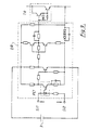
- Figure 1 is a schematic circuit diagram of one embodiment of the present invention;
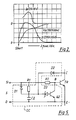
- Figure 2 is a waveform for explaining the operation of the circuit in Figure 1;
- Figure 3 is a detailed diagram of a base driving circuit with overcurrent protecting function;
- Figure 4 is a detailed diagram of a circuit in which the circuit in Figure 3 is provided with an alarm circuit;
- Figure 5 is a schematic diagram of a base driving circuit with overcurrent protecting function;
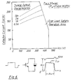
- Figure 6 is a diagram showing an example of Over Load Safety Operation Area of a power transistor;
- Figure 7 is an illustration of various types of short-circuit faults of an inverter;
- Figure 8 is a diagram showing an example of a conventional three phase bridge inverter circuit composition; and
- Figure 9 is a diagram showing an example of a composition of a conventional base driving circuit for a power transistor.
- Referring first to Figure 9, there is shown in detail the base driving circuit for a power transistor used as a power switching device similar to that described in the present applicant's US Patent US-A-4 949 213.
- US-A-4 949 213 describes a common drive output circuit for driving dissimilar switching semiconductor devices having different drive input characteristics by turning on and off dc power supplies to apply a voltage between the drive input terminals of either one of the switching semiconductor devices through two transistors connected in a Darlington pair, the collector circuit of one of the two transistors which is not at the output stage having a diode inserted in series which has such a polarity as to permit passage of the collector current.
- In Figure 9, TR indicates a pair of NPN power transistors in Darlington connection, DR indicates a base drive circuit, and the
numeral 3 designates a power supply of this base driving circuit (a driving power supply). The reference characters Si1 and Si2 refer to input terminals of a driving signal S which turns on and off the power transistor TR. In this circuit, the power transistor TR turns on when a photo-coupler PC1 turns on, and similarly the power transistor TR turns off when the photo-coupler PC1 turns off. - Figure 8 shows an example of an inverter circuit which comprises the base driving circuits as shown in Figure 9 and the power transistors.
- In Figure 8, TR1 to TR6 are NPN power transistors which are connected in bridge to form a three phase inverter, and IM denotes an induction motor. In this circuit, DC electric power applied between a positive line (+) LP and a negative line (-) LN of main DC electrodes is converted into three-phase AC electric power. The three phases, U, V, W, are supplied to the induction motor IM from each connection point (a midpoint) between the upper and lower arms of the bridge.
- When the base driving circuit DR as shown in Figure 9 is used in the inverter as shown in Figure 8, it requires three insulated
driving power supplies 3 each corresponding to a respective one of the transistors TR1, TR3 and TR5, because they are in the upper arms and the negative electrodes of thesedriving power supplies 3 are each coupled to different output lines of the three phase which differ in electrical potential from each other. - Compared with this, only one
driving power supply 3 may be required for the transistors TR2, TR4 and TR6 in the lower arms because the negative electrodes of thesedriving power supplies 3 are all coupled to the negative line (-) LN of the main circuit DC power supply, and are thus at the same electrical potential. That is, thedriving power supplies 3 in an inverter circuit in three phase bridge connection may consist of at least four power supplies, three for the upper arms and one for the lower arms. - In the inverter circuit as shown in Figure 8, short-circuit faults may occur such as an arm short-circuit, a series arm short-circuit, an output short-circuit or a ground. These are illustrated schematically in Figure 7.
- When these faults occur, an overcurrent flows through the power transistor TR. However, the power transistor has a Over Load Safe Operation Area (OLSOA) in its collector current ICP versus collector-emitter voltage VCE characteristic diagram as shown in Figure 6 and will not fail until the locus of ICP deviates from the OLSOA. Then, at a short-circuit fault the power transistors must be instantly brought into turn-off mode by detecting overcurrent by means of the circuit as shown in Figure 5.
- Figure 5 shows a schematic diagram of the base driving circuit with a function of overcurrent protection. In this diagram, the part enclosed by a broken line is an overcurrent protection circuit OC.
- The function of the power transistor protection in Figure 5 is as follows:
- 1. A driving signal S being applied to the terminals Si for turning on the power transistor charges a capacitor C1 through a resistor R1, and simultaneously turns on the power transistor TR through the resistor R2.
- 2. The normally operated power transistor TR has a much lower saturated collector-emitter voltage VCE(sat) than the avalanche voltage of a zener diode ZD. Then, the capacitor C1 discharges its charge to the collector C of the power transistor TR through a diode D2.
- 3. At a short circuit fault an excessive current that starts to flow in the power transistor TR raises VCE(sat) of TR to be higher than the avalanche voltage of the zener diode ZD. This prevents the capacitor C1 from discharging its charge to the power transistor TR.
- 4. As a result, the terminal voltage of the capacitor C1 is raised to be higher than the avalanche voltage of the zener diode ZD. This turns on an auxiliary transistor Q2 and lowers the base-emitter voltage of the power transistor TR to the saturated collector-emitter voltage VCE(sat) which turns off power transistor TR.
- Figure 3 shows a particular example of a circuit composition of the base driving (in this case, gate driving) circuit with overcurrent protecting function using an IGBT as a power switching device which is equivalent to the power transistor TR in Figure 5. In Figure 3 the part enclosed with a broken line is also an overcurrent protection circuit OC, and the other part is a base driving circuit DR. The basic function of the circuit in Figure 3 is the same as that in Figure 5, but the driving signal S is given through a photo-coupler PC1 as is the case in Figure 9, and the base driving circuit DR is more complex.
- The circuit as shown in Figure 3, however, lacks any means for providing an output on the functioning of the overcurrent protection circuit OC to the outside of the circuit. Then the circuit is usually provided with an alarm circuit ALMG, which is shown in Figure 4 as a part enclosed by a broken line. The overcurrent protection circuit in Figure 4, which is provided with an alarm circuit, is called an overcurrent protection circuit with alarm circuit OC1, for convenience.
- In an ordinary inverter circuit, an alarm signal ALM is applied to a driving signal generating circuit for cutting the driving signal S, which further turns off simultaneously six power device elements in a three phase inverter circuit to protect these power switching devices even if an overcurrent flows through only one of the chips of these power device elements.
- The overcurrent protection circuit described above has the problems now to be enumerated. When the driving circuit with alarm circuit in Figure 4 is used in a three phase inverter circuit such as is seen in Figure 8, the lines for alarm signals ALM for each power transistor must be insulated from each other for being collected together in order to supply the signals to an apparatus (a microcomputer, for example) which controls the driving signals for the six transistor elements, because the electrical potentials of the
driving power supplies 3 are different from each other for each of transistors TR1, TR3 and TR5 in the upper three arms and for all of transistors TR2, TR4 and TR6 in the lower three arms. Consequently, at least four photo-couplers in total, indicated as PC2 in Figure 4, are needed to provide an alarm function in the inverter circuit. This causes complexity of the circuit with the need for an increased number of components. - The present invention aims to solve the above problems and to provide a simplified protection circuit for a semiconductor device that permits the use of electronic components capable only of withstanding low voltages, thus reducing cost.
- According to the present invention, there is provided a semiconductor device, comprising a protection circuit, wherein said semiconductor device comprises power switching device chips each of which has a first and second main electrode and a control electrode for turning on and off a circuit between said first and second main electrodes, hereinafter referred to as a main circuit, in response to a control signal applied between said second main electrode and said control electrode, the first main electrode of one and the second main electrode of the other of respective pairs of said power switching device chips being connected together at midpoints to form series circuits in which said main circuits of two chips are connected in series with the same polarity, a number of said series circuits being contained in one package and being connected in parallel with the same polarity, and
- outputting an AC voltage supply from said midpoints between respective pairs of series-connected power switching device chips by applying a DC voltage between those main terminals of said switching device chips of each series connected pair which are not connected to said midpoints, and switching the power switching device chips on and off by applying driving signal pulses to their control electrodes
- said protection circuit further comprising:
- means, associated with each of the power switching device chips whose second main electrodes are connected to the midpoints, to detect overcurrents flowing in the associated power switching device chips and operative to render the respective power switching device chips non-conductive until the start of the next driving signal pulse applied to their respective control electrodes, the arrangement being such that successive periods of overcurrent flow cause the power switching device chip to heat up, temperature sensors being provided for detecting the temperature of each or a plurality of the power switching device chips whose second main electrodes are connected to said midpoints, the number of said temperature sensors (H) being equal to or less than the total number of such power switching device chips,
- means for generating a first alarm signal when the temperature detected by any of said temperature sensors exceeds a predetermined value, said means being coupled to a terminal point, hereinafter referred to as a point of reference potential, for said second main electrodes of said power switching device chip in each said series circuit, and the protection circuit comprising
- means for providing a second alarm signal by determining that the current of any of said main circuits in said power switching device chips whose second electrodes are connected to said point of reference potential, or a summed current of a plurality of said main circuits in these power switching device chips, exceeds a predetermined value, and
- means which receives the first and second alarm signals and emits a third alarm signal when one or more of said first and second alarm signals is detected.
- Overheating due to an overcurrent state is detected for power switching devices being at least in the upper arms of a bridged inverter circuit in Figure 8 by means of temperature sensors such as thermistors disposed in proximity to these devices through transmission lines electrically insulated from the devices.
- The preferred embodiment of the present invention is explained with reference to Figures 1 to 4. Figure 1 shows a schematic circuit as an example of the embodiments of the present invention. Figure 2 shows respective waveforms of a base current IB, a collector current IC and a collector-emitter voltage VCE of the power transistor during the overcurrent protection by the circuits in Figure 3 to Figure 5.
- In Figure 1, respective power transistors TR1 to TR6, which constitute an inverter circuit in a three phase bridge connection, are in this case power transistor chips, and these six chips are to be contained in one package. The overcurrent protection circuits OC for the power transistors TR1, TR3 and TR5 in the upper arms of the bridge, and a base driving circuit DR are the same as those in Figure 3 which do not emit alarm signals. On the other hand, the overcurrent protection circuits for the power transistors TR2, TR4 and TR6 in the lower arms of the bridge are those which emit alarm signals ALM1, and the overcurrent protection circuit with alarm circuit OC1 seen in Figure 4 may be used for them without any modification. This alarm signal ALM1, however, may be taken out directly from the alarm circuit without being relayed through a photo-coupler PC2, for example, from the collector of a transistor Q3 in the previous stage, because each emitter of these three power transistors TR2, TR4 and TR6 is coupled together to the negative line (-) LN of a main DC power supply which is on a point of reference potential. Then, in the present invention, the alarm photo-coupler PC2 may be eliminated from the overcurrent protection circuit with alarm circuit OC1 in Figure 4. These three alarm signals ALM1 are lead to the OR circuit G1. In the lower arms, the base driving circuits DR for the power transistors TR2, TR4 and TR6 are the same as those shown in Figure 3 or Figure 4.
- Temperature sensors H such as thermistors are disposed in proximity to the chips or elements of the power transistors TR1, TR3 and TR5. Each temperature sensor H is coupled to the OR circuit G1 through a respective overheat protection circuit OH, whose negative line is coupled to the negative line (-) LN of the main DC power supply on the point of reference potential.
- When an overcurrent flows through any one of the power transistors TR1, TR3 and TR5 in the upper arms, its collector current IC and emitter voltage VCE vary as shown in Figure 2 to cause the transistor element to become overheated. At the same time, the corresponding overcurrent protection circuit OC functions to turn off the driving signal which has been directly applied to the transistor, and this condition is latched as an OFF mode since the auxiliary transistor Q2 in OC is kept turned on by continuous discharging of the capacitor C1. The latching of the overcurrent protection circuit OC is then released when the pulsed driving signal S, which is given as an input signal to the base driving circuit DR of the transistor element, becomes OFF mode, since the capacitor C1 is not charged through the resistor R1 but discharges its charge through Q2 to reduce the terminal voltage below the avalanche voltage of the zener diode ZD to turn off Q2.
- Consequently, when the driving signal S becomes ON mode again to allow the overcurrent to flow, IC and VCE of the power transistor element have the same waveforms in Figure 2 again to reheat the power transistor element.
- By repeating such ON and OFF modes, those of the elements TR1, TR3 and TR5 through which the overcurrent flows are overheated, and when the temperature of an overheated element exceeds a predetermined value, the overheat protection circuit OH functions to give an alarm signal ALM2 to the OR circuit G1. Thus, the alarm signals due to overcurrent in any of the six power transistors TR1 to TR6 are given to the OR circuit G1. The output of this OR circuit G1, an alarm signal ALMO, is then given to a microcomputer not shown in the figure. The microcomputer gives the overcurrent protection circuits the driving signals S in OFF mode, which are transmitted to the six transistors through photo-couplers by signal transmission lines which are insulated from the main circuits. The six transistors TR1 to TR6 are then turned off simultaneously, and are thus protected.
- In the embodiment in Figure 1, power transistors are Used as switching devices, however, the switching devices are not limited to the power transistors but any power switching devices of the self-turn-off type may be applicable to the present invention.
- In addition, the number of the temperature sensors H may be less than that of the power transistors. At least two sensors H may be provided, accomplishing their purpose of overcurrent protection if the power transistors TR1, TR3 and TR5 are disposed in close proximity to allow the temperature sensors to be disposed among them so that overheating of any one of the power transistors TR1, TR3 or TR5 will be detected by the sensor.
- Furthermore, in Figure 1 the overcurrent protection circuits OC1 for the power transistors TR2, TR4 and TR6 in the lower arms of the bridge are provided for each power transistor element, but the purpose of the present invention may also be accomplished by, for example, coupling the emitters of the three power transistors TR2, TR4 and TR6 together to a terminal, inserting a shunt resistor between this terminal and the negative line (-) LN of main DC power supply, detecting increase of potential difference between both ends of this shunt resistor and transmitting this increase to only one overcurrent protection circuit which simultaneously turns off the three elements in the lower arms of the bridge to achieve the overcurrent protection.
- Another embodiment that may also be applied to the present invention is that which detects any of the VCE(sat) of the power transistors TR2, TR4 and TR6 exceeding a normal value by an overcurrent protection circuit which has three diodes D2 each coupled in parallel to the collectors of these three elements and effects overcurrent protection by turning them off simultaneously.
- Moreover, two different OR circuits may also be applied without departing from the scope of the present invention, one of which OR circuits receives the alarm signals ALM1 from the overcurrent protection circuits OC for the power transistors in the lower three arms, and the other OR circuit receiving the alarm signal ALM2 from the overheating protection circuit OH.
- The temperature sensors H are not always necessarily contained in the same package with TR1, TR3 and TR5, but may be disposed outside the package if these sensors are in positions that enable them effectively to detect overheating of TR1, TR3 and TR5.
- Utilising the teachings of this invention, it becomes unnecessary to provide the photo-couplers for outputting alarm signals for the overcurrent protection circuit of the power transistors in the upper arms, and components capable of withstanding only low voltages may be used.
Claims (2)
- A semiconductor device, comprising a protection circuit, wherein said semiconductor device comprises power switching device chips (TR1, TR2, TR3, TR4, TR5, TR6) each of which has a first and second main electrode and a control electrode for turning on and off a circuit between said first and second main electrodes, hereinafter referred to as a main circuit, in response to a control signal applied between said second main electrode and said control electrode, the first main electrode of one and the second main electrode of the other of respective pairs of said power switching device chips (TR1, TR2; TR3, TR4; TR5, TR6) being connected together at midpoints to form series circuits in which said main circuits of two chips are connected in series with the same polarity, a number of said series circuits being contained in one package and being connected in parallel with the same polarity, andoutputting an AC voltage supply from said midpoints between respective pairs of series-connected power switching device chips (TR1, TR2; TR3, TR4; TR5, TR6) by applying a DC voltage between those main terminals of said switching device chips of each series connected pair which are not connected to said midpoints, and switching the power switching device chips (TR1, TR2; TR3, TR4; TR5, TR6) on and off by applying driving signal pulses (S) to their control electrodessaid protection circuit further comprising:means (OC), associated with each of the power switching device chips (TR1, TR3, TR5) whose second main electrodes are connected to the midpoints, to detect overcurrents flowing in the associated power switching device chips (TR1, TR3, TR5) and operative to render the respective power switching device chips (TR1, TR3, TR5) non-conductive until the start of the next driving signal pulse (S) applied to their respective control electrodes, the arrangement being such that successive periods of overcurrent flow cause the power switching device chip (TR1, TR3, TR5) to heat up, temperature sensors (H) being provided for detecting the temperature of each or a plurality of the power switching device chips whose second main electrodes are connected to said midpoints, the number of said temperature sensors (H) being equal to or less than the total number of such power switching device chips (TR1, TR3, TR5),means (OH) for generating a first alarm signal (ALM2) when the temperature detected by any of said temperature sensors (H) exceeds a predetermined value, said means (OH) being coupled to a terminal point (LN), hereinafter referred to as a point of reference potential, for said second main electrodes of said power switching device chip (TR2, TR4, TR6) in each said series circuit, and the protection circuit comprisingmeans (OC1) for providing a second alarm signal (ALM1) by determining that the current of any of said main circuits in said power switching device chips (TR2, TR4, TR6) whose second electrodes are connected to said point of reference potential (LN), or a summed current of a plurality of said main circuits in these power switching device chips (TR2, TR4, TR6), exceeds a predetermined value, andmeans (G1) which receives the first and second alarm signals (ALM2, ALM1) and emits a third alarm signal (ALM0) when one or more of said first and second alarm signals is detected.
- A semiconductor device protection circuit, according to Claim 1, wherein three of said series circuits are contained in one package.
Applications Claiming Priority (2)
| Application Number | Priority Date | Filing Date | Title |
|---|---|---|---|
| JP45016/90 | 1990-02-26 | ||
| JP2045016A JP2811872B2 (en) | 1990-02-26 | 1990-02-26 | Semiconductor device protection circuit |
Publications (3)
| Publication Number | Publication Date |
|---|---|
| EP0444826A2 EP0444826A2 (en) | 1991-09-04 |
| EP0444826A3 EP0444826A3 (en) | 1992-12-16 |
| EP0444826B1 true EP0444826B1 (en) | 1996-10-02 |
Family
ID=12707558
Family Applications (1)
| Application Number | Title | Priority Date | Filing Date |
|---|---|---|---|
| EP91301408A Expired - Lifetime EP0444826B1 (en) | 1990-02-26 | 1991-02-21 | Protection circuit for a semiconductor device |
Country Status (5)
| Country | Link |
|---|---|
| US (1) | US5115388A (en) |
| EP (1) | EP0444826B1 (en) |
| JP (1) | JP2811872B2 (en) |
| KR (1) | KR0122309B1 (en) |
| DE (1) | DE69122419T2 (en) |
Families Citing this family (33)
| Publication number | Priority date | Publication date | Assignee | Title |
|---|---|---|---|---|
| JPH04285465A (en) * | 1991-03-13 | 1992-10-09 | Nec Corp | Switching power source with protective circuit |
| DE69314898T2 (en) * | 1992-08-28 | 1998-05-28 | Sgs Thomson Microelectronics | Overtemperature warning cycle when operating a multi-phase DC motor |
| DE19920505B4 (en) * | 1999-05-05 | 2004-05-27 | Semikron Elektronik Gmbh | Inverter with temperature balancing |
| JP3635988B2 (en) * | 1999-05-27 | 2005-04-06 | 富士電機デバイステクノロジー株式会社 | Semiconductor device |
| US6934139B2 (en) * | 2000-05-01 | 2005-08-23 | Fuji Electric Device Technology Co., Ltd. | Intelligent power module |
| US6968488B2 (en) | 2002-03-01 | 2005-11-22 | Broadcom Corporation | System and method for testing a circuit |
| FI116178B (en) * | 2002-08-22 | 2005-09-30 | Abb Oy | Arrangement for an output inductance coil in an inverter |
| DE10302811A1 (en) * | 2003-01-24 | 2004-08-12 | Siemens Ag | Circuit arrangement for protecting a power output stage with semiconductor switches |
| FI115266B (en) * | 2003-05-28 | 2005-03-31 | Abb Oy | Method and arrangement for parallel inverter modules |
| US6999329B2 (en) | 2003-04-25 | 2006-02-14 | Abb Oy | Temperature monitoring of parallel-connected inverter modules |
| FI116175B (en) * | 2003-12-19 | 2005-09-30 | Abb Oy | Method and device for protecting drives |
| US7110272B2 (en) * | 2004-06-22 | 2006-09-19 | Smc Electrical Products, Inc. | Inverter bridge controller implementing short-circuit protection scheme |
| JP2006280193A (en) * | 2005-03-03 | 2006-10-12 | Toyota Motor Corp | Drive circuit abnormality determination device, drive device including the same, and drive circuit abnormality determination method |
| JP4654940B2 (en) * | 2006-02-27 | 2011-03-23 | 株式会社デンソー | Inverter device and drive control method for inverter circuit |
| KR100827674B1 (en) * | 2006-05-23 | 2008-05-07 | (주)한빛테크 | Automatic trip device and control method |
| US8014118B2 (en) | 2007-02-27 | 2011-09-06 | Fuji Electric Systems Co., Ltd. | Load driving circuit, driver IC having a load driving circuit, and plasma display panel having a driver IC |
| CN101937888B (en) * | 2009-07-01 | 2013-01-23 | 辉达公司 | Circuit, system and method for controlling radiating of multiple units on circuit board |
| US20110018488A1 (en) * | 2009-07-22 | 2011-01-27 | Chia-Hsuan Lin | Frequency-changing control apparatus |
| TWI413358B (en) * | 2009-09-18 | 2013-10-21 | Sunonwealth Electr Mach Ind Co | Used for fan control systems |
| EP2560283A4 (en) * | 2010-04-14 | 2013-09-04 | Honda Motor Co Ltd | Short-circuit protection method |
| JP5360002B2 (en) | 2010-06-28 | 2013-12-04 | 富士電機株式会社 | Semiconductor device driving apparatus |
| JP5724730B2 (en) | 2010-12-14 | 2015-05-27 | 富士電機株式会社 | Semiconductor device driving apparatus |
| CN103460588B (en) * | 2011-04-08 | 2016-05-25 | 富士电机株式会社 | The control device of power inverter |
| DE102011076907B4 (en) * | 2011-06-01 | 2024-06-06 | Robert Bosch Gmbh | Method for operating an inverter and inverter |
| DE102011076908A1 (en) * | 2011-06-01 | 2012-12-06 | Robert Bosch Gmbh | Method for operating an inverter and inverters |
| JP2013220708A (en) * | 2012-04-16 | 2013-10-28 | Mitsubishi Heavy Ind Ltd | Heat medium heating device, and vehicle air conditioner equipped with the same |
| CN103809708A (en) | 2012-11-07 | 2014-05-21 | 辉达公司 | Panel electronic device, auxiliary heat dissipating device of panel electronic device and assembly of panel electronic device and auxiliary heat dissipating device |
| KR101412914B1 (en) * | 2012-11-22 | 2014-06-26 | 삼성전기주식회사 | Overheat protection circuit |
| US9673007B2 (en) | 2013-09-20 | 2017-06-06 | Maxim Integrated Products, Inc. | Systems and methods for discharging inductors with temperature protection |
| DE102014112760A1 (en) | 2013-09-20 | 2015-03-26 | Maxim Integrated Products, Inc. | Systems and methods for discharging inductors with temperature protection |
| US20170030962A1 (en) * | 2015-07-27 | 2017-02-02 | Hyundai Motor Company | Circuit for detecting failure of insulated gate bipolar transistor (igbt) power module |
| JP6398949B2 (en) * | 2015-11-05 | 2018-10-03 | 三菱電機株式会社 | Semiconductor device driving apparatus |
| JP7600565B2 (en) * | 2020-08-25 | 2024-12-17 | 富士電機株式会社 | Semiconductor Device |
Family Cites Families (11)
| Publication number | Priority date | Publication date | Assignee | Title |
|---|---|---|---|---|
| FR2252682A1 (en) * | 1973-11-22 | 1975-06-20 | Simplex Appareils | Electronic circuit-breaker for transformer - thermocouple and resistor detect large and small overloads |
| DD134705A1 (en) * | 1977-12-23 | 1979-03-14 | Wigand Gunther | PROTECTIVE CIRCUIT ARRANGEMENT FOR ELECTRICAL POWER CIRCUIT |
| DE2803557A1 (en) * | 1978-01-27 | 1979-08-02 | Bosch Gmbh Robert | DISCONNECTING DEVICE FOR A CONTROLLABLE SEMICONDUCTOR ELEMENT |
| JPS5928152B2 (en) * | 1978-11-04 | 1984-07-11 | ファナック株式会社 | Protection device for motor drive inverter circuit |
| DD155275A1 (en) * | 1980-12-15 | 1982-05-26 | Norbert Blacha | PROTECTION CIRCUIT FOR SEMICONDUCTOR INVERTER |
| US4360852A (en) * | 1981-04-01 | 1982-11-23 | Allis-Chalmers Corporation | Overcurrent and overtemperature protective circuit for power transistor system |
| JPS60121991A (en) * | 1983-12-02 | 1985-06-29 | Mitsubishi Electric Corp | Inverter controlled air conditioner |
| JPH0787247B2 (en) * | 1988-05-27 | 1995-09-20 | 三菱電機株式会社 | Semiconductor device |
| GB2221806B (en) * | 1988-06-27 | 1992-08-12 | Eaton Corp | Inverter short circuit protection method and apparatus |
| US4866559A (en) * | 1988-07-26 | 1989-09-12 | Texas Instruments Incorporated | Solid state circuit protector |
| US4965710A (en) * | 1989-11-16 | 1990-10-23 | International Rectifier Corporation | Insulated gate bipolar transistor power module |
-
1990
- 1990-02-26 JP JP2045016A patent/JP2811872B2/en not_active Expired - Fee Related
-
1991
- 1991-02-21 DE DE69122419T patent/DE69122419T2/en not_active Expired - Fee Related
- 1991-02-21 EP EP91301408A patent/EP0444826B1/en not_active Expired - Lifetime
- 1991-02-26 US US07/661,513 patent/US5115388A/en not_active Expired - Lifetime
- 1991-02-26 KR KR1019910003057A patent/KR0122309B1/en not_active Expired - Fee Related
Also Published As
| Publication number | Publication date |
|---|---|
| US5115388A (en) | 1992-05-19 |
| JPH03247114A (en) | 1991-11-05 |
| KR920000166A (en) | 1992-01-10 |
| EP0444826A3 (en) | 1992-12-16 |
| KR0122309B1 (en) | 1997-11-22 |
| DE69122419D1 (en) | 1996-11-07 |
| EP0444826A2 (en) | 1991-09-04 |
| DE69122419T2 (en) | 1997-03-06 |
| JP2811872B2 (en) | 1998-10-15 |
Similar Documents
| Publication | Publication Date | Title |
|---|---|---|
| EP0444826A2 (en) | Protection circuit for a semiconductor device | |
| US5200878A (en) | Drive circuit for current sense igbt | |
| EP0680147B1 (en) | Semiconductor power module and power conversion device | |
| US4949213A (en) | Drive circuit for use with voltage-drive semiconductor device | |
| US5210479A (en) | Drive circuit for an insulated gate transistor having overcurrent detecting and adjusting circuits | |
| EP0814564A1 (en) | Electronic switching circuit with reduction of switching transients | |
| US5365397A (en) | Device for protecting power semiconductor device against short circuit | |
| GB2161337A (en) | Protection circuit | |
| JPH08307221A (en) | Circuit for controlling power mos gate type circuit | |
| KR19980071760A (en) | Circuit and Method for Improving IGBT Short Circuit Capacity | |
| EP0556379B1 (en) | Motor controller | |
| JPS63501119A (en) | Method and apparatus for sensing short circuits in motor control circuits | |
| EP0580180B1 (en) | Charging circuit capable of supplying DC voltage directly to power supply circuit when battery is removed | |
| US5764466A (en) | Circuit for short circuit detection through resistive shunt in power circuits using unipolar control voltage | |
| JP4739541B2 (en) | AC chopper device | |
| US4945358A (en) | Short circuit protection arrangement for a driver circuit | |
| JP3226084B2 (en) | Power transistor overcurrent limiting circuit | |
| US5216349A (en) | Driving circuit for a switching element including an improved power supply arrangement | |
| EP0363020B1 (en) | Driving circuit | |
| JP3713795B2 (en) | Output circuit of control device | |
| US5091688A (en) | Remotely switched voltage converter | |
| JPH03106217A (en) | Driving circuit for isolate gate transistor, overcurrent detection circuit and semiconductor | |
| US4731550A (en) | Circuit having a feed circuit for supplying current to a load resistor | |
| KR940005929Y1 (en) | Power regulator circuit | |
| KR930007653Y1 (en) | Inverter |
Legal Events
| Date | Code | Title | Description |
|---|---|---|---|
| PUAI | Public reference made under article 153(3) epc to a published international application that has entered the european phase |
Free format text: ORIGINAL CODE: 0009012 |
|
| AK | Designated contracting states |
Kind code of ref document: A2 Designated state(s): DE FR GB |
|
| PUAL | Search report despatched |
Free format text: ORIGINAL CODE: 0009013 |
|
| AK | Designated contracting states |
Kind code of ref document: A3 Designated state(s): DE FR GB |
|
| 17P | Request for examination filed |
Effective date: 19930220 |
|
| 17Q | First examination report despatched |
Effective date: 19940214 |
|
| GRAG | Despatch of communication of intention to grant |
Free format text: ORIGINAL CODE: EPIDOS AGRA |
|
| GRAH | Despatch of communication of intention to grant a patent |
Free format text: ORIGINAL CODE: EPIDOS IGRA |
|
| GRAH | Despatch of communication of intention to grant a patent |
Free format text: ORIGINAL CODE: EPIDOS IGRA |
|
| GRAA | (expected) grant |
Free format text: ORIGINAL CODE: 0009210 |
|
| AK | Designated contracting states |
Kind code of ref document: B1 Designated state(s): DE FR GB |
|
| REF | Corresponds to: |
Ref document number: 69122419 Country of ref document: DE Date of ref document: 19961107 |
|
| ET | Fr: translation filed | ||
| PLBE | No opposition filed within time limit |
Free format text: ORIGINAL CODE: 0009261 |
|
| STAA | Information on the status of an ep patent application or granted ep patent |
Free format text: STATUS: NO OPPOSITION FILED WITHIN TIME LIMIT |
|
| 26N | No opposition filed | ||
| PGFP | Annual fee paid to national office [announced via postgrant information from national office to epo] |
Ref country code: DE Payment date: 19991231 Year of fee payment: 10 |
|
| PGFP | Annual fee paid to national office [announced via postgrant information from national office to epo] |
Ref country code: FR Payment date: 20000210 Year of fee payment: 10 |
|
| PGFP | Annual fee paid to national office [announced via postgrant information from national office to epo] |
Ref country code: GB Payment date: 20000216 Year of fee payment: 10 |
|
| PG25 | Lapsed in a contracting state [announced via postgrant information from national office to epo] |
Ref country code: GB Free format text: LAPSE BECAUSE OF NON-PAYMENT OF DUE FEES Effective date: 20010221 |
|
| GBPC | Gb: european patent ceased through non-payment of renewal fee |
Effective date: 20010221 |
|
| PG25 | Lapsed in a contracting state [announced via postgrant information from national office to epo] |
Ref country code: FR Free format text: LAPSE BECAUSE OF NON-PAYMENT OF DUE FEES Effective date: 20011031 |
|
| REG | Reference to a national code |
Ref country code: FR Ref legal event code: ST |
|
| PG25 | Lapsed in a contracting state [announced via postgrant information from national office to epo] |
Ref country code: DE Free format text: LAPSE BECAUSE OF NON-PAYMENT OF DUE FEES Effective date: 20011201 |