EP0444836A2 - Verfahren zur Herstellung von Isolationszonen für Halbleiteranordnungen - Google Patents
Verfahren zur Herstellung von Isolationszonen für Halbleiteranordnungen Download PDFInfo
- Publication number
- EP0444836A2 EP0444836A2 EP91301457A EP91301457A EP0444836A2 EP 0444836 A2 EP0444836 A2 EP 0444836A2 EP 91301457 A EP91301457 A EP 91301457A EP 91301457 A EP91301457 A EP 91301457A EP 0444836 A2 EP0444836 A2 EP 0444836A2
- Authority
- EP
- European Patent Office
- Prior art keywords
- trench
- film
- polycrystalline silicon
- oxide film
- silicon
- Prior art date
- Legal status (The legal status is an assumption and is not a legal conclusion. Google has not performed a legal analysis and makes no representation as to the accuracy of the status listed.)
- Granted
Links
Images


Classifications
-
- H—ELECTRICITY
- H10—SEMICONDUCTOR DEVICES; ELECTRIC SOLID-STATE DEVICES NOT OTHERWISE PROVIDED FOR
- H10W—GENERIC PACKAGES, INTERCONNECTIONS, CONNECTORS OR OTHER CONSTRUCTIONAL DETAILS OF DEVICES COVERED BY CLASS H10
- H10W10/00—Isolation regions in semiconductor bodies between components of integrated devices
- H10W10/40—Isolation regions comprising polycrystalline semiconductor materials
-
- H—ELECTRICITY
- H10—SEMICONDUCTOR DEVICES; ELECTRIC SOLID-STATE DEVICES NOT OTHERWISE PROVIDED FOR
- H10P—GENERIC PROCESSES OR APPARATUS FOR THE MANUFACTURE OR TREATMENT OF DEVICES COVERED BY CLASS H10
- H10P14/00—Formation of materials, e.g. in the shape of layers or pillars
- H10P14/60—Formation of materials, e.g. in the shape of layers or pillars of insulating materials
- H10P14/61—Formation of materials, e.g. in the shape of layers or pillars of insulating materials using masks
-
- H—ELECTRICITY
- H10—SEMICONDUCTOR DEVICES; ELECTRIC SOLID-STATE DEVICES NOT OTHERWISE PROVIDED FOR
- H10W—GENERIC PACKAGES, INTERCONNECTIONS, CONNECTORS OR OTHER CONSTRUCTIONAL DETAILS OF DEVICES COVERED BY CLASS H10
- H10W10/00—Isolation regions in semiconductor bodies between components of integrated devices
- H10W10/01—Manufacture or treatment
- H10W10/011—Manufacture or treatment of isolation regions comprising dielectric materials
- H10W10/012—Manufacture or treatment of isolation regions comprising dielectric materials using local oxidation of silicon [LOCOS]
-
- H—ELECTRICITY
- H10—SEMICONDUCTOR DEVICES; ELECTRIC SOLID-STATE DEVICES NOT OTHERWISE PROVIDED FOR
- H10W—GENERIC PACKAGES, INTERCONNECTIONS, CONNECTORS OR OTHER CONSTRUCTIONAL DETAILS OF DEVICES COVERED BY CLASS H10
- H10W10/00—Isolation regions in semiconductor bodies between components of integrated devices
- H10W10/01—Manufacture or treatment
- H10W10/041—Manufacture or treatment of isolation regions comprising polycrystalline semiconductor materials
-
- H—ELECTRICITY
- H10—SEMICONDUCTOR DEVICES; ELECTRIC SOLID-STATE DEVICES NOT OTHERWISE PROVIDED FOR
- H10W—GENERIC PACKAGES, INTERCONNECTIONS, CONNECTORS OR OTHER CONSTRUCTIONAL DETAILS OF DEVICES COVERED BY CLASS H10
- H10W10/00—Isolation regions in semiconductor bodies between components of integrated devices
- H10W10/10—Isolation regions comprising dielectric materials
- H10W10/13—Isolation regions comprising dielectric materials formed using local oxidation of silicon [LOCOS], e.g. sealed interface localised oxidation [SILO] or side-wall mask isolation [SWAMI]
Definitions
- the present invention relates to a process for forming isolation regions for electrically isolating devices constituting semiconductor integrated circuits, and more particularly to a process for forming trench isolation regions by forming device isolation trenches in a semiconductor substrate and refilling the trenches with an insulation film.
- the isolation regions for isolating the devices from one another have become gradually narrower.
- 4 Mb DRAMs are 1.0 to 0.8 ⁇ m
- 16 Mb DRAMs are 0.8 to 0.6 ⁇ m
- 64 Mb DRAMs will be reduced to 0.5 to 0.4 ⁇ m.
- the device isolation regions having a width of at least 0.6 ⁇ m can be formed by local oxidation of silicon isolation (LOCOS process) or improved LOCOS process.
- LOCOS process is such that a silicon nitride film covering a silicon substrate is apertured by patterning, and the exposed silicon substrate surface is selectively oxidized to form a silicon oxide film serving as an insulation film.
- the LOCOS process is unable to form isolation regions of up to 0.5 ⁇ m. Unless the oxide film on the isolation regions is made extremely thin, the LOCOS process permits oxidation of the silicon substrate to progress to regions covered with the silicon nitride film to result in side-wise extensions of silicon oxide film called bird's beaks. Thus, the isolation regions spread out beyond the mask size, making it impossible to form narrow isolation regions.
- the so-called trench isolation process has been proposed.
- a resist pattern formed by lithography is used as an etching mask to form recessed trenches in a silicon substrate, and the trenches are filled up with an insulator such as a silicon oxide film.
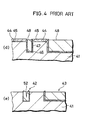
- FIG. 4 is a diagram showing the conventional trench isolation process, which will be described with reference to FIG. 4.
- the use of the trench isolation process forms trench regions which only serve as the isolation regions, so that the isolation width can be reduced to a value limited by lithography.
- the trench isolation process is therefore suitable for isolation the devices of semiconductor integrated circuits of increased packing densities.
- the oxide film 48 deposited in the step (2) is as thick as about 1 ⁇ m.
- LP CVD Low Pressure Vapor Deposition
- the oxide film will be overetched by 800 angstroms at portions where the etching proceeds at the highest rate, even if the in-plane uniformity of the equal-rate etching condition for the resin film and the oxide film is within ⁇ 2% Accordingly, unless the rate of etching of the polycrystalline silicon film 45 is very small under the equal-rate etching condition, the active regions also are etched and thereby damaged. Even if the etching is stopped at the polycrystalline silicon film 45 as desired, a distinct step with a height of about 800 angstroms will occur between the isolation region and the active region.
- the treatment with hydrofluoric acid creates a wedgelike minute ditch 52 in the center of the trench 42 with a large aspect ratio.
- the formation of the isolation regions is followed by the formation of the gate insulation film and gate electrode wiring for MOS transistors.
- the presence of the minute ditch 52 in the isolation region entails the problem of a break in the wiring, or a short circuit between the wirings, which would occur if the wiring material remains in the minute ditch.
- An object of the present invention is to overcome the problems peculiar to the conventional trench isolation process, such as impairment of electrical characteristics due to etching damage, impairment of transistor characteristics due to a step produced on a border between an active region and isolation region, or short circuits between the wirings due to a minute ditch produced in the center of an isolation region,. and to provide a relatively simple isolation process with trench isolation technology, which is suitable for semiconductor integrated circuits with increased packing density.
- the present invention provides a process for forming a semiconductor device isolation region which comprises: a) forming on a silicon substrate at least a first thin silicon oxide film and a first silicon nitride film thereon, b) etching the substrate using a resist pattern to form a trench for providing an isolation region, c) forming a second silicon oxide film and a second silicon nitride film on the side walls and bottom wall of the trench, d) subsequently forming a first polycrystalline silicon film on the substrate including the trench, leaving the first polycrystalline silicon film only on the side walls of the trench by anisotropic etching, and thereafter oxidizing the remaining first polycrystalline silicon film to form an oxide film on the side walls of the trench, and e) further forming a second polycrystalline silicon film over the semiconductor substrate including the trench, leaving the second polycrystalline silicon film only between the oxide film portions on the side walls of the trench by anisotropic etching, and thereafter oxidizing the remaining second polycrystalline silicon film to thereby form an oxide film
- the process of the present invention does not include the step of depositing a thick oxide film and etching back the oxide film. Therefore, the present process is free from the damage of the active region and steps between the active region and the device isolation region, which induced by the overetching.
- the first polycrystalline silicon film may have a thickness of about 0.1 ⁇ m corresponding to about 1/4 of a minimum trench width, and hte second polycrystalline silicon film may have a thickness of about one-half of the depth of the trench.
- Such thin polycrystalline silicon films can be etched under conditions with a large selectivity relative to the underlying oxide film and nitride film. This remarkably diminishes the likelihood of causing damage to the active region and eliminates a large step at the boundary between the active region and the trench, consequently precluding the impairment of the electrical characteristics and the impairment of the transistor threshold characteristics.
- the first and second polycrystalline silicon films are much thinner than the 1 ⁇ m-thick oxide film used in the conventional trench isolation process, so that the silicon films can be deposited within a short time to achieve an improved throughput.
- the LOCOS oxidation for wide isolation regions can be done at the same time of the second polycrystalline silicon oxidation.
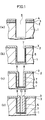
- FIG. 1 is a process diagram showing a first embodiment of the invention for forming device isolation regions. The embodiment will be described below with reference to FIG. 1. The following steps (a), (b), (c), (d), (e), (f), (g) and (h) correspond to FIG. 1, (a), (b), (c), (d), (e), (f), (g) and (h), respectively.
- MOS transistors and other device are formed on the surface of the silicon substrate 1 by the known process.
- device isolation regions having a very small width of 0.5 ⁇ m were formed. Further N-type MOS transistors (not shown) were formed, which had a channel length of 0.5 ⁇ m and the isolation regions of very small width. When the transistors were tested, no increase in the junction leak current was found as compared with that of transistors separated by the conventional LOCOS process. Further, despite the isolation width of 0.5 ⁇ m, the leak current of the parasitic MOS transistors was not larger than the conventional level. Additionally, the transistors operated with satisfactory characteristics despite the channel width of 0.5 ⁇ m which was not available by the LOCOS process.
- FIG. 2 shows a process diagram of the second embodiment of the present invention.
- the steps of the present embodiment illustrated in FIG. 2, (a), (b), (c), (d), (e), (f), (g) and (h) correspond to the steps of FIG. 1, (a), (b), (c), (d), (e), (f), (g) and (h), respectively, with the exception of the following feature. Therefore, a detailed description will not be given.
- the present embodiment employs the polycrystalline silicon pad LOCOS process which is an improvement of the LOCOS process, and in this respect, the embodiment differs from the first embodiment.
- a polycrystalline silicon film 21 serving as a pad is formed between the thin oxide film 2 and the nitride film 3 in the step (a).
- the present embodiment had the same advantages as the first embodiment.
- FIG. 3 shows the process of the third embodiment.
- the following steps of the present embodiment (a), (b), (c), (d), (e), (f), (g) and (h) correspond to the steps of FIG. 3, (a), (b), (c), (d), (e), (f), (g) and (h), respectively.
- the present embodiment also employs the polycrystalline silicon pad LOCOS process which is an improvement of the LOCOS process.
- the oxidation for wide isolation is done separately from the oxidation of the second polycrystalline silicon film.
- MOS transistors and other devices are formed on the surface of the silicon substrate 1 by the known process.
- the present embodiment also had the same advantages as the fist embodiment described.
- the process of the present invention does not include the steps, peculiar to the convention trench isolation process, of depositing a thick oxide film and etching back the thick film. So, the present process is therefore free from damage of the active region and steps at the boundary between the active region and the trench isolation region, which are induced by the overetching. This precludes impairment of the electrical characteristics due to etching damage to the active region and impairment of the device characteristics due to imperfect flatness.
- first and second polycrystalline silicon films are thinner than the 1 ⁇ m-thick oxide film used in the conventional trench isolation process.
- the film deposition time can therefore be shorter to achieve an improved throughput.
- polycrystalline silicon is buried in the trench and then oxidized to form an oxide film in the trench.
- This method obviates a minute ditch at the center of the trench, which is inevitable to CVD-oxide film filled in trench. Consequently, the method prevents short circuits between the wirings.
- the semiconductor devices when integrated circuits are fabricated using the process of the present invention, the semiconductor devices can be insulated and isolated satisfactorily by very small isolation regions, so that the present process contributes to great improvements in the packing density and provides integrated circuits in high yields with high reliability.
- wide isolation regions can be oxidized by the LOCOS process concurrently with the oxidation of the polycrystalline silicon film. This leads to the advantage that device isolation regions with varying widths can be formed efficiently.
Landscapes
- Element Separation (AREA)
- Semiconductor Memories (AREA)
- Local Oxidation Of Silicon (AREA)
Applications Claiming Priority (3)
| Application Number | Priority Date | Filing Date | Title |
|---|---|---|---|
| JP2043393A JP2597022B2 (ja) | 1990-02-23 | 1990-02-23 | 素子分離領域の形成方法 |
| JP43393/90 | 1990-02-23 | ||
| JP4339390 | 1990-02-23 |
Publications (3)
| Publication Number | Publication Date |
|---|---|
| EP0444836A2 true EP0444836A2 (de) | 1991-09-04 |
| EP0444836A3 EP0444836A3 (en) | 1991-11-06 |
| EP0444836B1 EP0444836B1 (de) | 2000-04-19 |
Family
ID=12662547
Family Applications (1)
| Application Number | Title | Priority Date | Filing Date |
|---|---|---|---|
| EP91301457A Expired - Lifetime EP0444836B1 (de) | 1990-02-23 | 1991-02-22 | Verfahren zur Herstellung von Isolationszonen für Halbleiteranordnungen |
Country Status (5)
| Country | Link |
|---|---|
| US (1) | US5116779A (de) |
| EP (1) | EP0444836B1 (de) |
| JP (1) | JP2597022B2 (de) |
| KR (1) | KR950000102B1 (de) |
| DE (1) | DE69132118T2 (de) |
Cited By (3)
| Publication number | Priority date | Publication date | Assignee | Title |
|---|---|---|---|---|
| EP0635884A1 (de) * | 1993-07-13 | 1995-01-25 | Siemens Aktiengesellschaft | Verfahren zur Herstellung eines Grabens in einem Substrat und dessen Verwendung in der Smart-Power-Technologie |
| US5700712A (en) * | 1993-06-23 | 1997-12-23 | Siemens Aktiengesellschaft | Method for manufacturing an insulating trench in an SOI substrate for smartpower technologies |
| EP0853338A1 (de) * | 1997-01-09 | 1998-07-15 | Texas Instruments Incorporated | Verbesserungen im Bezug auf Halbleiteranordnungen |
Families Citing this family (28)
| Publication number | Priority date | Publication date | Assignee | Title |
|---|---|---|---|---|
| US5399516A (en) * | 1992-03-12 | 1995-03-21 | International Business Machines Corporation | Method of making shadow RAM cell having a shallow trench EEPROM |
| EP0631305B1 (de) * | 1993-06-23 | 1998-04-15 | Siemens Aktiengesellschaft | Verfahren zur Herstellung eines Isolationsgrabens in einem Substrat für Smart-Power-Technologien |
| EP0641022B1 (de) * | 1993-08-31 | 2006-05-17 | STMicroelectronics, Inc. | Isolationsstruktur und Verfahren zur Herstellung |
| JP3022714B2 (ja) * | 1993-10-29 | 2000-03-21 | 日本電気株式会社 | 半導体装置およびその製造方法 |
| US5438016A (en) * | 1994-03-02 | 1995-08-01 | Micron Semiconductor, Inc. | Method of semiconductor device isolation employing polysilicon layer for field oxide formation |
| TW274628B (de) * | 1994-06-03 | 1996-04-21 | At & T Corp | |
| US5478758A (en) * | 1994-06-03 | 1995-12-26 | At&T Corp. | Method of making a getterer for multi-layer wafers |
| US5455194A (en) * | 1995-03-06 | 1995-10-03 | Motorola Inc. | Encapsulation method for localized oxidation of silicon with trench isolation |
| KR0147630B1 (ko) * | 1995-04-21 | 1998-11-02 | 김광호 | 반도체 장치의 소자분리방법 |
| KR100361761B1 (ko) * | 1995-06-02 | 2003-02-05 | 주식회사 하이닉스반도체 | 반도체소자의소자분리절연막형성방법 |
| KR100214068B1 (ko) * | 1995-11-21 | 1999-08-02 | 김영환 | 반도체 장치의 소자분리막 형성방법 |
| US5933746A (en) | 1996-04-23 | 1999-08-03 | Harris Corporation | Process of forming trench isolation device |
| US6037239A (en) * | 1997-04-23 | 2000-03-14 | Elantec, Inc. | Method for making a contact structure for a polysilicon filled trench isolation |
| US6057209A (en) * | 1997-07-10 | 2000-05-02 | Advanced Micro Devices, Inc. | Semiconductor device having a nitrogen bearing isolation region |
| US6136664A (en) * | 1997-08-07 | 2000-10-24 | International Business Machines Corporation | Filling of high aspect ratio trench isolation |
| US5976950A (en) * | 1997-11-13 | 1999-11-02 | National Semiconductor Corporation | Polysilicon coated swami (sidewall masked isolation) |
| US6118167A (en) * | 1997-11-13 | 2000-09-12 | National Semiconductor Corporation | Polysilicon coated nitride-lined shallow trench |
| KR100253406B1 (ko) | 1998-01-20 | 2000-04-15 | 김영환 | 반도체 파워 집적회로에서의 소자격리구조 및 그 방법 |
| US5989977A (en) * | 1998-04-20 | 1999-11-23 | Texas Instruments - Acer Incorporated | Shallow trench isolation process |
| US6037018A (en) * | 1998-07-01 | 2000-03-14 | Taiwan Semiconductor Maufacturing Company | Shallow trench isolation filled by high density plasma chemical vapor deposition |
| TW400605B (en) * | 1999-01-16 | 2000-08-01 | United Microelectronics Corp | The manufacturing method of the Shallow Trench Isolation (STI) |
| US6500729B1 (en) * | 2000-06-02 | 2002-12-31 | Agere Systems Guardian Corp. | Method for reducing dishing related issues during the formation of shallow trench isolation structures |
| US6573154B1 (en) * | 2000-10-26 | 2003-06-03 | Institute Of Microelectronics | High aspect ratio trench isolation process for surface micromachined sensors and actuators |
| DE10234165B4 (de) * | 2002-07-26 | 2008-01-03 | Advanced Micro Devices, Inc., Sunnyvale | Verfahren zum Füllen eines Grabens, der in einem Substrat gebildet ist, mit einem isolierenden Material |
| US6933206B2 (en) * | 2003-10-10 | 2005-08-23 | Infineon Technologies Ag | Trench isolation employing a high aspect ratio trench |
| JP4657614B2 (ja) * | 2004-03-09 | 2011-03-23 | Okiセミコンダクタ株式会社 | 半導体装置及び半導体装置の製造方法 |
| US7776708B1 (en) * | 2005-08-11 | 2010-08-17 | National Semiconductor Corporation | System and method for providing a nitride cap over a polysilicon filled trench to prevent formation of a vertical bird's beak structure in the manufacture of a semiconductor device |
| US7863153B1 (en) | 2006-07-13 | 2011-01-04 | National Semiconductor Corporation | System and method for creating different field oxide profiles in a locos process |
Family Cites Families (12)
| Publication number | Priority date | Publication date | Assignee | Title |
|---|---|---|---|---|
| JPS58175843A (ja) * | 1982-04-08 | 1983-10-15 | Matsushita Electric Ind Co Ltd | 半導体集積回路の製造方法 |
| JPS59135743A (ja) * | 1983-01-24 | 1984-08-04 | Hitachi Ltd | 半導体装置およびその製造方法 |
| JPS59227136A (ja) * | 1983-06-08 | 1984-12-20 | Matsushita Electronics Corp | 半導体装置の製造方法 |
| JPS6054453A (ja) * | 1983-09-05 | 1985-03-28 | Oki Electric Ind Co Ltd | 半導体集積回路装置の製造方法 |
| US4666557A (en) * | 1984-12-10 | 1987-05-19 | Ncr Corporation | Method for forming channel stops in vertical semiconductor surfaces |
| US4671851A (en) * | 1985-10-28 | 1987-06-09 | International Business Machines Corporation | Method for removing protuberances at the surface of a semiconductor wafer using a chem-mech polishing technique |
| US4666556A (en) * | 1986-05-12 | 1987-05-19 | International Business Machines Corporation | Trench sidewall isolation by polysilicon oxidation |
| GB2200794A (en) * | 1986-11-19 | 1988-08-10 | Plessey Co Plc | Semiconductor device manufacture |
| JP2590867B2 (ja) * | 1987-03-27 | 1997-03-12 | ソニー株式会社 | メモリ装置の製造方法 |
| JPS63314844A (ja) * | 1987-06-18 | 1988-12-22 | Toshiba Corp | 半導体装置の製造方法 |
| JPS6445165A (en) * | 1987-08-13 | 1989-02-17 | Toshiba Corp | Semiconductor device and manufacture thereof |
| US4876214A (en) * | 1988-06-02 | 1989-10-24 | Tektronix, Inc. | Method for fabricating an isolation region in a semiconductor substrate |
-
1990
- 1990-02-23 JP JP2043393A patent/JP2597022B2/ja not_active Expired - Fee Related
-
1991
- 1991-02-20 US US07/657,770 patent/US5116779A/en not_active Expired - Lifetime
- 1991-02-22 KR KR1019910002883A patent/KR950000102B1/ko not_active Expired - Lifetime
- 1991-02-22 DE DE69132118T patent/DE69132118T2/de not_active Expired - Lifetime
- 1991-02-22 EP EP91301457A patent/EP0444836B1/de not_active Expired - Lifetime
Cited By (4)
| Publication number | Priority date | Publication date | Assignee | Title |
|---|---|---|---|---|
| US5700712A (en) * | 1993-06-23 | 1997-12-23 | Siemens Aktiengesellschaft | Method for manufacturing an insulating trench in an SOI substrate for smartpower technologies |
| EP0635884A1 (de) * | 1993-07-13 | 1995-01-25 | Siemens Aktiengesellschaft | Verfahren zur Herstellung eines Grabens in einem Substrat und dessen Verwendung in der Smart-Power-Technologie |
| US5445988A (en) * | 1993-07-13 | 1995-08-29 | Siemens Aktiengesellschaft | Method for manufacturing a trench in a substrate for use in smart-power technology |
| EP0853338A1 (de) * | 1997-01-09 | 1998-07-15 | Texas Instruments Incorporated | Verbesserungen im Bezug auf Halbleiteranordnungen |
Also Published As
| Publication number | Publication date |
|---|---|
| DE69132118T2 (de) | 2000-09-28 |
| KR950000102B1 (ko) | 1995-01-09 |
| US5116779A (en) | 1992-05-26 |
| JPH03245553A (ja) | 1991-11-01 |
| JP2597022B2 (ja) | 1997-04-02 |
| DE69132118D1 (de) | 2000-05-25 |
| EP0444836A3 (en) | 1991-11-06 |
| EP0444836B1 (de) | 2000-04-19 |
Similar Documents
| Publication | Publication Date | Title |
|---|---|---|
| US5116779A (en) | Process for forming semiconductor device isolation regions | |
| US5786263A (en) | Method for forming a trench isolation structure in an integrated circuit | |
| KR960016502B1 (ko) | 집적 회로 분리 방법 | |
| US5989977A (en) | Shallow trench isolation process | |
| US6524931B1 (en) | Method for forming a trench isolation structure in an integrated circuit | |
| US6277709B1 (en) | Method of forming shallow trench isolation structure | |
| KR100224700B1 (ko) | 반도체장치의 소자분리방법 | |
| US6825544B1 (en) | Method for shallow trench isolation and shallow trench isolation structure | |
| US5192706A (en) | Method for semiconductor isolation | |
| JP3076772B2 (ja) | 半導体素子の素子分離膜形成方法 | |
| US4903107A (en) | Buried oxide field isolation structure with composite dielectric | |
| US6355539B1 (en) | Method for forming shallow trench isolation | |
| US20010012675A1 (en) | Shallow trench isolation process | |
| KR19990061066A (ko) | 반도체소자의 소자분리막 형성방법 | |
| US7018927B2 (en) | Method for forming isolation film for semiconductor devices | |
| US5952707A (en) | Shallow trench isolation with thin nitride as gate dielectric | |
| KR100596876B1 (ko) | 반도체 소자의 소자 분리막 형성 방법 | |
| KR100195237B1 (ko) | 개선된 트렌치와 로코스 조합형 소자분리방법 | |
| KR100305026B1 (ko) | 반도체소자의 제조방법 | |
| US6261966B1 (en) | Method for improving trench isolation | |
| KR100235971B1 (ko) | 반도체 소자의 제조방법 | |
| KR0172240B1 (ko) | 반도체 소자의 소자분리 방법 | |
| KR100429555B1 (ko) | 반도체 소자의 트렌치형 소자분리막 형성방법 | |
| US6716720B2 (en) | Method for filling depressions on a semiconductor wafer | |
| KR19990057375A (ko) | 반도체 소자의 소자분리막 형성방법 |
Legal Events
| Date | Code | Title | Description |
|---|---|---|---|
| PUAI | Public reference made under article 153(3) epc to a published international application that has entered the european phase |
Free format text: ORIGINAL CODE: 0009012 |
|
| 17P | Request for examination filed |
Effective date: 19910315 |
|
| AK | Designated contracting states |
Kind code of ref document: A2 Designated state(s): DE FR GB |
|
| PUAL | Search report despatched |
Free format text: ORIGINAL CODE: 0009013 |
|
| AK | Designated contracting states |
Kind code of ref document: A3 Designated state(s): DE FR GB |
|
| 17Q | First examination report despatched |
Effective date: 19920410 |
|
| GRAG | Despatch of communication of intention to grant |
Free format text: ORIGINAL CODE: EPIDOS AGRA |
|
| GRAG | Despatch of communication of intention to grant |
Free format text: ORIGINAL CODE: EPIDOS AGRA |
|
| GRAG | Despatch of communication of intention to grant |
Free format text: ORIGINAL CODE: EPIDOS AGRA |
|
| GRAH | Despatch of communication of intention to grant a patent |
Free format text: ORIGINAL CODE: EPIDOS IGRA |
|
| GRAH | Despatch of communication of intention to grant a patent |
Free format text: ORIGINAL CODE: EPIDOS IGRA |
|
| GRAA | (expected) grant |
Free format text: ORIGINAL CODE: 0009210 |
|
| AK | Designated contracting states |
Kind code of ref document: B1 Designated state(s): DE FR GB |
|
| REF | Corresponds to: |
Ref document number: 69132118 Country of ref document: DE Date of ref document: 20000525 |
|
| ET | Fr: translation filed | ||
| PLBE | No opposition filed within time limit |
Free format text: ORIGINAL CODE: 0009261 |
|
| STAA | Information on the status of an ep patent application or granted ep patent |
Free format text: STATUS: NO OPPOSITION FILED WITHIN TIME LIMIT |
|
| 26N | No opposition filed | ||
| REG | Reference to a national code |
Ref country code: GB Ref legal event code: IF02 |
|
| PGFP | Annual fee paid to national office [announced via postgrant information from national office to epo] |
Ref country code: FR Payment date: 20100223 Year of fee payment: 20 |
|
| PGFP | Annual fee paid to national office [announced via postgrant information from national office to epo] |
Ref country code: DE Payment date: 20100303 Year of fee payment: 20 Ref country code: GB Payment date: 20100202 Year of fee payment: 20 |
|
| REG | Reference to a national code |
Ref country code: DE Ref legal event code: R071 Ref document number: 69132118 Country of ref document: DE |
|
| REG | Reference to a national code |
Ref country code: GB Ref legal event code: PE20 Expiry date: 20110221 |
|
| PG25 | Lapsed in a contracting state [announced via postgrant information from national office to epo] |
Ref country code: GB Free format text: LAPSE BECAUSE OF EXPIRATION OF PROTECTION Effective date: 20110221 |
|
| PG25 | Lapsed in a contracting state [announced via postgrant information from national office to epo] |
Ref country code: DE Free format text: LAPSE BECAUSE OF EXPIRATION OF PROTECTION Effective date: 20110222 |