EP0444925B1 - Circuit de stabilisation d'image - Google Patents
Circuit de stabilisation d'image Download PDFInfo
- Publication number
- EP0444925B1 EP0444925B1 EP19910301634 EP91301634A EP0444925B1 EP 0444925 B1 EP0444925 B1 EP 0444925B1 EP 19910301634 EP19910301634 EP 19910301634 EP 91301634 A EP91301634 A EP 91301634A EP 0444925 B1 EP0444925 B1 EP 0444925B1
- Authority
- EP
- European Patent Office
- Prior art keywords
- signals
- output
- section
- circuit
- synchronising
- Prior art date
- Legal status (The legal status is an assumption and is not a legal conclusion. Google has not performed a legal analysis and makes no representation as to the accuracy of the status listed.)
- Expired - Lifetime
Links
- 230000003019 stabilising effect Effects 0.000 title claims description 18
- 238000000926 separation method Methods 0.000 claims description 29
- 230000001629 suppression Effects 0.000 claims description 13
- 238000000034 method Methods 0.000 claims description 10
- 230000008929 regeneration Effects 0.000 claims description 10
- 238000011069 regeneration method Methods 0.000 claims description 10
- 239000003990 capacitor Substances 0.000 claims description 3
- 230000010354 integration Effects 0.000 claims 2
- 230000000903 blocking effect Effects 0.000 claims 1
- 239000003086 colorant Substances 0.000 description 3
- 230000003111 delayed effect Effects 0.000 description 2
- 238000010586 diagram Methods 0.000 description 2
- 238000006243 chemical reaction Methods 0.000 description 1
- 238000001514 detection method Methods 0.000 description 1
- 230000009977 dual effect Effects 0.000 description 1
- 238000000605 extraction Methods 0.000 description 1
- 230000008570 general process Effects 0.000 description 1
- 230000007274 generation of a signal involved in cell-cell signaling Effects 0.000 description 1
- 238000002955 isolation Methods 0.000 description 1
- 238000004519 manufacturing process Methods 0.000 description 1
- 230000008569 process Effects 0.000 description 1
- 230000000153 supplemental effect Effects 0.000 description 1
- 230000001960 triggered effect Effects 0.000 description 1
Images

Classifications
-
- H—ELECTRICITY
- H04—ELECTRIC COMMUNICATION TECHNIQUE
- H04N—PICTORIAL COMMUNICATION, e.g. TELEVISION
- H04N9/00—Details of colour television systems
- H04N9/64—Circuits for processing colour signals
- H04N9/641—Multi-purpose receivers, e.g. for auxiliary information
Definitions
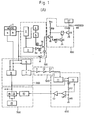
- the present invention relates to a picture regeneration stabilising circuit, and particularly to the operation of such a circuit during a non-signal input (non-inputting) or blanking period in order to stabilise the colours of the picture by preventing discrimination errors caused by gating noise when discriminating the broadcasting method during tape regeneration (playback).
- a discriminating section 400 which includes a B.G.P. delaying detecting section 11, a burst gate 12, an OP amplifier OP1 and a buffer 13 is supplied to the PAL/MESECAM detection section 10.
- the signals are supplied to the OP amplifier OP1 where the signals are compared with the reference voltages of the supply resistances R7,R8.
- the B.G.P signals will be described as a supplemental matter. That is, the B.G.P signals are needed for the following reason.
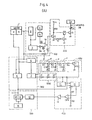
- the present invention is intended to overcome the above described disadvantages of the conventional circuit by the provision of a picture regeneration stabilising circuit with dual suppression circuits.
- the further suppression circuit is controlled by the output of a synchronising signal isolator of the Y/C separation section, and the Y/C separation section is adapted to output synchronising signals (B.G.P.) in the presence of a line/tuner video signal input, and to output a high voltage in the absence of such input signals.
- a synchronising signal isolator of the Y/C separation section is adapted to output synchronising signals (B.G.P.) in the presence of a line/tuner video signal input, and to output a high voltage in the absence of such input signals.
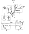
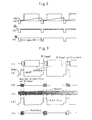
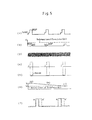
- the signals supplied as described above will behave in such a manner that the synchronising (B.G.P.) signals and the chroma signals which have passed respectively through the delay section 500 and the chroma drive section 8 will be supplied to the discriminating section 400 in the normal manner, because the supplied signal (wave pattern 2 of Figure 5) corresponds to (lies below) the active reference level of the transistor Q1, and consequently the transistor Q1 is turned off.
- a high voltage is output instead of a synchronising (B.G.P.) signal from the synchronising isolator 7 of the Y/C separation section 300 (when there is no signal input, the power source voltage is output because of the inherent nature of the synchronising isolator).
- This high voltage is supplied to the base of the synchronising (B.G.P.) and colour muting transistor Q1 in the form of the wave pattern 6 of Figure 5, after passing through the integrating circuits d,e,f consisting respectively of resistance R1, capacitance C1, resistance R2, capacitance C2, resistance R3 and capacitance C3.
Landscapes
- Engineering & Computer Science (AREA)
- Multimedia (AREA)
- Signal Processing (AREA)
- Processing Of Color Television Signals (AREA)
Claims (7)
- Circuit de stabilisation d'image destiné à recevoir des signaux vidéo de syntoniseur/ligne et à stabiliser un signal d'image particulièrement pendant un blocage de signal, comprenant:une section (100) de séparation de synchronisation de syntoniseur destiné à recevoir des signaux vidéo (b) de syntoniseur et à fournir un signal de sortie indiquant si les signaux vidéo de syntoniseur sont en cours de réception;un circuit (200) de suppression vidéo devant être commandé par le signal de sortie de la section (100) de séparation de synchronisation de syntoniseur et destiné à empêcher les interférences syntoniseur/ligneune section (300) de séparation Y/C destinée à recevoir les signaux vidéo de syntoniseur/ligne et à effectuer une séparation Y/C;une section de discrimination (400) destinée à recevoir des signaux de synchronisation (B. G. P) et les signaux de chroma séparés par la section (300) de séparation Y/C, à détecter les signaux de salve de synchronisation de sous-porteuse et les signaux de reconnaissance et à comparer les signaux détectés avec une tension de référence pour produire un signal de sortie; etune section (700) de discrimination de procédé de télédiffusion pour discriminer et sélectionner le procédé de télédiffusion en se basant sur le signal de sortie de la section de discrimination (400), le circuit de stabilisation comprenant, en outre:un circuit supplémentaire (600) de suppression destiné à neutraliser les signaux de chroma et les signaux de synchronisation (B.G.P) fournis à la section de discrimination (400) pendant un blocage de signal.
- Circuit de stabilisation d'image selon la revendication 1, dans lequel le circuit supplémentaire (600) de suppression est commandé par le signal de sortie d'un dispositif d'isolation de signal de synchronisation (7) de la section (300) de séparation Y/C; et
la section (300) de séparation Y/C est adaptée pour fournir des signaux de synchronisation (B.G.P) en présence d'un signal d'entrée vidéo ligne/syntoniseur, et pour fournir une haute tension en l'absence de ces signaux d'entrée. - Circuit de stabilisation d'image selon la revendication 2, dans lequel le circuit de suppression supplémentaire (600) comprend:un circuit d'intégration (d, e, f) pour exécuter une intégration après réception du signal de sortie dudit dispositif d'isolation de synchronisation (7) de la section (300) de séparation Y/C, etun transistor (Q1) de suppression de chrominance commandé par le signal intégré par le circuit d'intégration (d, e, f) pour bloquer les impulsions de synchronisation (B.G.P) et les signaux de chrominance fournis par ailleurs à la section de discrimination (400) pendant une période de blocage de signal ou période de suppression.
- Circuit de stabilisation de regénération d'image selon la revendication 3, dans lequel le circuit d'intégration consiste en trois circuits (d.e.f) d'intégration et d'égalisation de courant continu montés en série, chaque circuit d'intégration et d'égalisation de courant continu (d, e, f) consistant en une résistance et un condensateur monté entre la sortie de cette résistance et la terre.
- Circuit de stabilisation de régénération d'image selon la revendication 3 ou 4, dans lequel le transistor (Q1) de suppression de chrominance a son collecteur connecté, via une résistance (R5), de manière à former une sortie et à fournir un signal à la section de discrimination (400), et son émetteur connecté à la terre.
- Circuit de stabilisation de régénération d'image selon l'une quelconque des revendications précédentes et comprenant, en outre, une ligne à retard (500) par l'intermédiaire de laquelle les signaux de chroma et de synchronisation (B.G.P) sont fournis à partir de la section de séparation Y/C à la section de discrimination (400).
- Circuit de stabilisation de regénération d'image selon l'une quelconque des revendications précédentes, dans lequel la section de discrimination comprend un amplificateur de sortie (18, OP1).
Applications Claiming Priority (2)
| Application Number | Priority Date | Filing Date | Title |
|---|---|---|---|
| KR900002373 | 1990-02-28 | ||
| KR237390 | 1990-02-28 |
Publications (3)
| Publication Number | Publication Date |
|---|---|
| EP0444925A2 EP0444925A2 (fr) | 1991-09-04 |
| EP0444925A3 EP0444925A3 (en) | 1993-05-19 |
| EP0444925B1 true EP0444925B1 (fr) | 1997-02-05 |
Family
ID=19296401
Family Applications (1)
| Application Number | Title | Priority Date | Filing Date |
|---|---|---|---|
| EP19910301634 Expired - Lifetime EP0444925B1 (fr) | 1990-02-28 | 1991-02-28 | Circuit de stabilisation d'image |
Country Status (1)
| Country | Link |
|---|---|
| EP (1) | EP0444925B1 (fr) |
Family Cites Families (2)
| Publication number | Priority date | Publication date | Assignee | Title |
|---|---|---|---|---|
| FR2428362A1 (fr) * | 1978-06-09 | 1980-01-04 | Thomson Csf | Circuit de decodage des informations de chrominance, dans le systeme de television secam, et recepteur de television comportant un tel circuit |
| JPS62227291A (ja) * | 1986-03-29 | 1987-10-06 | Toshiba Corp | 自動色飽和度制御装置 |
-
1991
- 1991-02-28 EP EP19910301634 patent/EP0444925B1/fr not_active Expired - Lifetime
Also Published As
| Publication number | Publication date |
|---|---|
| EP0444925A3 (en) | 1993-05-19 |
| EP0444925A2 (fr) | 1991-09-04 |
Similar Documents
| Publication | Publication Date | Title |
|---|---|---|
| CA1252880A (fr) | Recepteur de television multi-standard | |
| US7805056B2 (en) | Methods and apparatus for providing cycles of normal and non normal phase in a color burst signal | |
| EP0084241B1 (fr) | Dispositif de traitement de signal et méthode pour enregistrer sur une bande vidéo | |
| DK143728B (da) | Lodret synkroniseringskredsloeb for fjernsynsmodtagere | |
| JPH0566076B2 (fr) | ||
| EP0444925B1 (fr) | Circuit de stabilisation d'image | |
| EP0342634A2 (fr) | Circuit et méthode de génération de l'impulsion d'attaque verticale dans un récepteur de signal vidéo | |
| US4015287A (en) | Color television receiver including a chrominance subcarrier regenerator | |
| JP3092938B2 (ja) | 画像表示装置用ディジタル同期回路 | |
| US5815213A (en) | Video signal synchronization extraction device | |
| US7777813B2 (en) | Color burst automatic detection device | |
| JP2619524B2 (ja) | ゴースト検出用基準信号の抽出回路 | |
| KR900000126B1 (ko) | 다중시스템 텔레비젼 수신기 | |
| KR910005705Y1 (ko) | Pal/secam방식의 자동 색신호 제거회로 | |
| KR940011032B1 (ko) | 자동 선국 구동장치 | |
| US7432918B2 (en) | Video signal processing circuit | |
| JPS5825779A (ja) | 多方式カラ−テレビジヨン受像機 | |
| CA1262281A (fr) | Recepteur de television multisysteme | |
| JPH0723304A (ja) | 映像信号選択回路の信号検出回路 | |
| JP3456712B2 (ja) | 複合映像信号検出回路 | |
| JPS628628Y2 (fr) | ||
| US5122867A (en) | Video signal processing circuit having a band pass filter following a delay circuit in a comb filter arrangement | |
| KR910004904Y1 (ko) | 상관관계 검출에 의한 점 노이즈 제거회로 | |
| KR0131601Y1 (ko) | 2수평 주기 지연부를 이용한 팔 방식/세캄 방식 판별회로 | |
| JPS54161231A (en) | Color television receiver |
Legal Events
| Date | Code | Title | Description |
|---|---|---|---|
| PUAI | Public reference made under article 153(3) epc to a published international application that has entered the european phase |
Free format text: ORIGINAL CODE: 0009012 |
|
| AK | Designated contracting states |
Kind code of ref document: A2 Designated state(s): DE FR GB |
|
| PUAL | Search report despatched |
Free format text: ORIGINAL CODE: 0009013 |
|
| AK | Designated contracting states |
Kind code of ref document: A3 Designated state(s): DE FR GB |
|
| 17P | Request for examination filed |
Effective date: 19930908 |
|
| 17Q | First examination report despatched |
Effective date: 19950818 |
|
| GRAG | Despatch of communication of intention to grant |
Free format text: ORIGINAL CODE: EPIDOS AGRA |
|
| GRAH | Despatch of communication of intention to grant a patent |
Free format text: ORIGINAL CODE: EPIDOS IGRA |
|
| GRAH | Despatch of communication of intention to grant a patent |
Free format text: ORIGINAL CODE: EPIDOS IGRA |
|
| GRAA | (expected) grant |
Free format text: ORIGINAL CODE: 0009210 |
|
| AK | Designated contracting states |
Kind code of ref document: B1 Designated state(s): DE FR GB |
|
| REF | Corresponds to: |
Ref document number: 69124535 Country of ref document: DE Date of ref document: 19970320 |
|
| ET | Fr: translation filed | ||
| PLBE | No opposition filed within time limit |
Free format text: ORIGINAL CODE: 0009261 |
|
| STAA | Information on the status of an ep patent application or granted ep patent |
Free format text: STATUS: NO OPPOSITION FILED WITHIN TIME LIMIT |
|
| 26N | No opposition filed | ||
| REG | Reference to a national code |
Ref country code: GB Ref legal event code: IF02 |
|
| PGFP | Annual fee paid to national office [announced via postgrant information from national office to epo] |
Ref country code: FR Payment date: 20100223 Year of fee payment: 20 |
|
| PGFP | Annual fee paid to national office [announced via postgrant information from national office to epo] |
Ref country code: GB Payment date: 20100224 Year of fee payment: 20 Ref country code: DE Payment date: 20100312 Year of fee payment: 20 |
|
| REG | Reference to a national code |
Ref country code: DE Ref legal event code: R071 Ref document number: 69124535 Country of ref document: DE |
|
| REG | Reference to a national code |
Ref country code: GB Ref legal event code: PE20 Expiry date: 20110227 |
|
| PG25 | Lapsed in a contracting state [announced via postgrant information from national office to epo] |
Ref country code: GB Free format text: LAPSE BECAUSE OF EXPIRATION OF PROTECTION Effective date: 20110227 |
|
| PG25 | Lapsed in a contracting state [announced via postgrant information from national office to epo] |
Ref country code: DE Free format text: LAPSE BECAUSE OF EXPIRATION OF PROTECTION Effective date: 20110228 |