EP0445664A2 - Circuit de détection d'oscillations caractéristiques - Google Patents
Circuit de détection d'oscillations caractéristiques Download PDFInfo
- Publication number
- EP0445664A2 EP0445664A2 EP91103089A EP91103089A EP0445664A2 EP 0445664 A2 EP0445664 A2 EP 0445664A2 EP 91103089 A EP91103089 A EP 91103089A EP 91103089 A EP91103089 A EP 91103089A EP 0445664 A2 EP0445664 A2 EP 0445664A2
- Authority
- EP
- European Patent Office
- Prior art keywords
- oscillation
- signal
- frequency
- pass filter
- pilot carrier
- Prior art date
- Legal status (The legal status is an assumption and is not a legal conclusion. Google has not performed a legal analysis and makes no representation as to the accuracy of the status listed.)
- Granted
Links
- 230000010355 oscillation Effects 0.000 claims abstract description 87
- 238000001514 detection method Methods 0.000 claims abstract description 38
- 230000001360 synchronised effect Effects 0.000 claims abstract description 14
- 230000005236 sound signal Effects 0.000 claims abstract description 10
- 230000001419 dependent effect Effects 0.000 claims abstract description 3
- 238000001914 filtration Methods 0.000 claims abstract description 3
- 239000003990 capacitor Substances 0.000 claims description 7
- 238000005516 engineering process Methods 0.000 claims description 7
- 238000010586 diagram Methods 0.000 description 11
- 230000005540 biological transmission Effects 0.000 description 5
- 239000013078 crystal Substances 0.000 description 2
- 238000000034 method Methods 0.000 description 2
- 239000004065 semiconductor Substances 0.000 description 2
- 230000015572 biosynthetic process Effects 0.000 description 1
- 238000013016 damping Methods 0.000 description 1
- 238000004519 manufacturing process Methods 0.000 description 1
- 239000010453 quartz Substances 0.000 description 1
- VYPSYNLAJGMNEJ-UHFFFAOYSA-N silicon dioxide Inorganic materials O=[Si]=O VYPSYNLAJGMNEJ-UHFFFAOYSA-N 0.000 description 1
- 238000011144 upstream manufacturing Methods 0.000 description 1
Images

Classifications
-
- H—ELECTRICITY
- H03—ELECTRONIC CIRCUITRY
- H03D—DEMODULATION OR TRANSFERENCE OF MODULATION FROM ONE CARRIER TO ANOTHER
- H03D1/00—Demodulation of amplitude-modulated oscillations
- H03D1/22—Homodyne or synchrodyne circuits
- H03D1/2281—Homodyne or synchrodyne circuits using a phase locked loop
-
- H—ELECTRICITY
- H04—ELECTRIC COMMUNICATION TECHNIQUE
- H04N—PICTORIAL COMMUNICATION, e.g. TELEVISION
- H04N5/00—Details of television systems
- H04N5/44—Receiver circuitry for the reception of television signals according to analogue transmission standards
- H04N5/60—Receiver circuitry for the reception of television signals according to analogue transmission standards for the sound signals
- H04N5/607—Receiver circuitry for the reception of television signals according to analogue transmission standards for the sound signals for more than one sound signal, e.g. stereo, multilanguages
Definitions
- the invention relates to a circuit arrangement for detecting characteristic oscillations with which a pilot carrier oscillation is amplitude-modulated in a television audio signal, with an input filter stage for filtering out a predetermined frequency band around the frequency of the pilot carrier oscillation, an amplitude detection stage for demodulating the modulated pilot carrier oscillation, and a low-pass filter for suppressing high-frequency signal components at the output of the amplitude detection stage and one detection branch for each characteristic oscillation, which is connected downstream of the low-pass filter.
- stereo decoders for television and radio receivers in switched capacitor technology which have an identification branch for identifying the transmission type "two-channel" or “Stereo".
- This identification branch comprises a continuously operating low-pass filter for suppressing signal components that could cause interference in the useful signal in subsequent mixing operations, and - in switch capacitor technology - a pilot carrier filter, which is designed as a high-pass filter, suppresses the sound information and amplifies the pilot carrier.
- a pilot carrier filter which is designed as a high-pass filter, suppresses the sound information and amplifies the pilot carrier.
- An AM detector and a low-pass filter Two identification filters for the frequencies 117.5 Hz and 274.1 Hz are connected to the output of the low-pass filter. The output levels of these filters are detected using first order peak detectors and low pass filters. The comparators are used Output signals of the first-order low-pass filters are converted into switching levels adapted for subsequent digital signal processing.
- the known circuit arrangement is very complex due to the use of several filters.
- these filters have relatively large bandwidths, so that in addition to the characteristic oscillations of 117.5 Hz and 274.1 Hz, interference is transmitted which makes it difficult to clearly identify the type of transmission.
- the object of the invention is to provide a circuit arrangement in the simplest possible embodiment for this purpose.
- a limiter amplifier is arranged between the low-pass filter and the detection branches and in that each detection branch comprises: a digital phase-locked loop with a narrow-band capture range around the frequency of the characteristic oscillation to be detected for generating a reference oscillation from the signals at the output of the amplitude detection stage, a digital synchronous demodulator for demodulating the signal supplied by the limiter amplifier with the reference oscillation, and a digital integrator for summing up counting pulses when a predetermined value of the output signal of the digital synchronous demodulator over a predetermined time interval and for delivering an identification signal which is dependent on the sum of the counting pulses achieved.
- the circuit arrangement according to the invention thus advantageously avoids the difficulty of providing narrow-band filters, which necessarily require a high level of technical complexity. Rather, simple circuits, which only have to process a digital signal with a word length of one bit, achieve an arbitrarily narrow-band selection of the characteristic oscillations and thus any interference-free identification of the type of transmission.
- circuit arrangement according to the invention has only three filters, the quality of which, however, is essentially only subject to minimal requirements.
- the entire circuit arrangement can also be integrated on a semiconductor body without exception, so that external components are eliminated. As a result of this and due to the lack of adjustment, very cost-effective production and assembly with reliable function is possible.
- an input filter stage 1 is supplied with a television audio signal via an input 11 which, in addition to audio information, also comprises a pilot carrier oscillation, preferably with a frequency of 54.7 kHz.
- the pilot carrier oscillation is amplitude-modulated with a characteristic oscillation; the associated characteristic oscillation has a frequency of 117.5 Hz for the stereo mode and a frequency of 274.1 Hz for the two-tone mode. In mono mode, the pilot carrier vibration is unmodulated.
- the input filter stage 1 comprises a high-pass filter 12, to which the television audio signal is fed from the input 11, and a downstream band-pass filter, preferably implemented using switch capacitor technology and matched to the frequency of the pilot carrier oscillation.
- the high-pass filter 12, which is preferably designed as a continuously operating stage, is designed with respect to its cutoff frequency in such a way that the audio information in the television audio signal is at least largely suppressed and thus no longer occurs at the input of the bandpass filter 13. Since the frequency of the pilot carrier oscillation is significantly higher than the highest frequency in the sound information, a high-pass filter of a simple design and therefore of limited quality is sufficient for this purpose.
- the bandpass filter 13 filters out the pilot carrier oscillation and the characteristic oscillations modulated on it from the remaining television audio signal. Since the sound information is already at least largely suppressed by the upstream high-pass filter 12, there are at most medium demands on the selectivity of the bandpass filter 13, which can therefore also be implemented as a simple circuit arrangement.
- the one Formation of the bandpass 13 clock signal required in switch capacitor technology is supplied via a clock signal input 14.
- the pilot carrier oscillation amplitude-modulated with the respective characteristic oscillation is output.
- the bandpass filter 13 has a bandwidth of approximately 1 kHz. This ensures, on the one hand, that the characteristic vibrations occurring as side lines of the pilot carrier vibration for the two-tone operation of 274.1 Hz are at least largely passed through without damping, while vibrations with a greater frequency spacing from the pilot carrier vibration are effectively suppressed as disturbances.
- the modulated pilot carrier oscillation is fed to an input 20 of the amplitude detection stage 2.
- This comprises a digital phase locked loop 21 which is matched to the pilot carrier oscillation and to which this is fed via a limiter amplifier 22 in order to generate a reference oscillation.
- the limiter amplifier 22 forms a rectangular signal from the modulated pilot carrier oscillation, which has an essentially circular function, which serves as the input signal of the digital phase locked loop 21.
- the digital phase-locked loop 21 generates a square-wave signal from the frequency of the pilot carrier oscillation, which is used as a reference oscillation in the amplitude detection stage 2, in a manner to be described in more detail below.
- This reference oscillation is fed to an analog mixing stage 23, likewise encompassed by the amplitude detection stage 2, at its reference oscillation input 24, while the modulated pilot carrier oscillation is for mixing with the reference oscillation is fed to a signal input 25 of the analog mixing stage 23.
- the characteristic oscillation modulated onto the pilot carrier oscillation is then available as a demodulated signal.
- the analog mixing stage is preferably designed as a double balanced mixer.
- the characteristic oscillations obtained therein by amplitude synchronous demodulation are fed to the detection branches 4 and 5 via the low-pass filter 3 and a limiter amplifier 6.
- the low-pass filter 3 preferably has a cut-off frequency of 300 Hz, so that the characteristic oscillations of 117.5 Hz or 274.1 Hz can be supplied to the detection branches 4 and 5 at least almost undamped, while higher-frequency mixed products, harmonics and other disturbances are suppressed.
- the low-pass filter 3 is also preferably implemented using switch capacitor technology and, since no high requirements have to be made for compliance with the cut-off frequency, can also be simple.
- the low-pass filter 3 is preferably supplied with the clock signal also supplied to the bandpass filter 13 via the clock signal input 14 via a clock signal input 30.
- a clock signal of lower frequency can also be fed to the clock signal input 30.
- the output 60 of the limiter amplifier 6 for the characteristic oscillations there is, depending on the operating mode, a square-wave signal derived from the respective characteristic oscillation with a frequency of 117.5 Hz in the stereo mode or 274.1 Hz in the two-tone mode for forwarding to the detection branches 4, 5 available. No characteristic oscillation occurs in the case of mono mode.
- the pilot carrier oscillation preferably 54.7 kHz can then be completely eliminated, i.e. it does not need to be broadcast by the broadcaster.
- Each of the detection branches 4 and 5 which in principle have an identical structure, but are tuned to the different frequencies of the characteristic vibrations, contains a digital phase-locked loop 40 or 50 with a narrow-band capture range around the frequency of the characteristic vibration to be detected, i.e. around 117.5 Hz in the digital Phase locked loop 40 of the stereo detection branch 4 and around 274.1 Hz in the digital phase locked loop 50 of the two-tone detection branch 5.
- Each of the digital phase locked loops 40 and 50 receives the signals output at the output 60 of the limiter amplifier 6 at its inputs 41 and 51, respectively.
- the digital phase-locked loops 40 and 50 respectively a square-wave signal with the frequency of the assigned characteristic oscillation starts at its outputs 42 and 52.
- the signal referred to as the reference oscillation is fed to a first input 43 or 53 of a digital synchronous demodulator 44 or 54, which receives the signal supplied unchanged from the output 60 of the limiter amplifier 6 at its second input 45 or 55.
- This signal is demodulated in the associated synchronous demodulator 44 or 54 with the reference oscillation by the corresponding digital phase locked loop 40 or 50 and then fed to a digital integrator 47 or 57 via a line 46 or 56.
- the digital synchronous demodulators 44, 54 each comprise an exclusive-OR gate. This only delivers a signal with a constant level via line 46 if the inputs 43, 45 or 53, 55 of the digital synchronous demodulators 44 or 54 are supplied with signals of the same frequency. However, this is only the case if the vibrations offered via the output 60 of the limiter amplifier 6 have frequencies within the capture range of the associated digital phase locked loop 40 or 50.
- the digital integrators 47 and 57 preferably each comprise a counting circuit, to which 48 and 58 counting pulses are supplied via counting pulse inputs. These digital pulses are summed in the digital integrators 47, 57 when a predetermined value of the output signal of the associated digital synchronous demodulator 44 or 54 occurs on the lines 46 or 56 over a predetermined time interval. If a certain counting position is reached or exceeded in one of the integrators 47, 57 during or at the end of the predetermined time interval, the corresponding integrator 47 or 57 outputs an identification signal at an identification signal output 49 or 59, which indicates the operating mode indicates in which the received and processed television audio signal is transmitted.
- the counting position at which the identification signal occurs can be specified as a fraction of the maximum sum of the counting pulses that can be achieved in the predetermined time interval.
- the integrators 47, 57 suppress brief interferences on the lines 46, 56 due to noise or beats.
- the capture range of the digital phase-locked loops is preferably 40 or 50 1 Hz, arranged symmetrically to the frequencies of the characteristic oscillations.
- the digital integrators 47, 57 extend these catch ranges symmetrically again by 1 Hz, so that the recognition branches 4 and 5 only accept oscillations in a frequency range of 2 Hz around the frequency of the associated identification oscillations as characteristic oscillations.
- the digital integrators 47, 57 are then dimensioned with large time constants of approximately one second.
- the dimensioning of the time constant and the so-called identification window, ie the frequency range of the vibrations accepted as the characteristic vibration are coordinated with one another in order to enable reliable detection of detected characteristic vibrations.
- the described design of the detection branches also has the advantage that the identification window can be dimensioned arbitrarily, even narrower, so that not only noise mixed down into the baseband, but also crosstalk of image or sound signals can be suppressed.
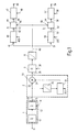
- FIG. 2 shows a block diagram to explain the function of the digital phase-locked loops 21, 40 and 50 using the example of the digital phase-locked loop 40.
- This includes a sample and hold element 401 for storing the value of the phase-locked loop 40 via the input 41 supplied signal when an edge occurs in a control signal which is present at the sample and hold element 401 via a control input 404.
- the current of the two signal levels, which the signal supplied by the limiter amplifier 6 can accept, is stored on each edge of the control signal.
- a frequency divider 402 which can be switched between two divisors will divide the frequency of a reference oscillation supplied to the frequency divider 402 via a reference input 403.
- the frequency-divided signal appears at the output 406 of the frequency divider 402 and on the one hand forms the control signal for the control input 404 and on the other hand the reference oscillation for the output 42 of the digital phase locked loop 40.
- FIG. 3 shows in partial diagram a) the time course of the rectangular characteristic oscillation emitted by the limiter amplifier 6, as is fed to the input 41 of the phase locked loop 40 when the stereo operating mode is present.
- part diagram b the reference oscillation generated by phase-locked loop 40 is sketched, namely in the left part of the diagram in the non-synchronized state of the phase-locked loop, while the right part of the diagram shows the state in which the phase-locked loop runs synchronously with the characteristic oscillation, ie snapped onto it.
- t is the time.
- t1 to t7 are the times at which an edge occurs in the control signal at the control input 404, ie the current value of the signal at the input 41 is stored by the sample and hold element 401.
- the digital phase-locked loop runs freely and is therefore not locked in place. Accordingly, a low signal value (times t1, t2) is stored several times by the sample and hold element 401 in the example shown.
- frequency divider 402 the frequency of the reference oscillation from reference input 403 is then divided by the larger of the two divisors, n2.
- the period of the control signal at output 406 is greater than the period of the characteristic oscillation supplied at input 41. The edges in the control signal, ie the times t1, t2, thus shift gradually to later phase positions of the signal at input 41.
- a state is reached in which the edge in the control signal arrives at the control input 404 at a point in time in which the signal at the input 41 no longer has a low value but has now assumed a high value.
- this value now reverses the frequency divider 402 in such a way that the reference oscillation from the reference input 403 is divided by the smaller of the two divisors, n1.
- the period of the control signal is correspondingly shortened until its next edge, at which in turn the value of the signal at the input 41 is sampled.
- This time t4 is again in the diagram according to FIG. 3 such that a low value is sampled there in the signal at input 41. This divides the reference oscillation again by the divisor n2.
- the locked state In the locked state, the stored values alternate continuously from one edge in the control signal to the next, so that the frequency of the reference oscillation is alternately divided between two successive edges in the control signal by the first and second divisors n1 and n2.
- this locked state can only be achieved if the frequency of the signal at input 41 between the two frequency values defined by the frequency of the reference oscillation and the values of the divisors n1 and n2, which form the limits of the capture range.
- the capture range of the digital phase locked loop 40 can thus be chosen as desired.
- the phase locked loops 21 and 50 also have reference inputs 213 and 503, respectively.
- the reference inputs 403, 503 and 213 are preferably supplied with the same reference oscillation or a signal derived from the same reference oscillation.
- clock signals are advantageously derived from the reference oscillation, which are fed to the bandpass filter 13 and the low-pass filter 3 at the associated clock signal input 14 or 30.
- the counting pulses at the counting pulse inputs 48, 58 can also be derived from the reference oscillation. Then only a single frequency standard is required for the circuit arrangement according to FIG. 1, so that the entire arrangement that can be integrated on a semiconductor crystal is coupled as the only external component with only one quartz crystal.
- the capture range of the digital phase-locked loop 21 in the amplitude detection stage 2 is also made as narrow as possible.
- the capture range is selected to be approximately 300 Hz, for example. It can preferably be made just wide enough that fluctuations in the frequency of the pilot carrier oscillation, which can occur as a result of certain line interruptions in the transmission systems providing the television audio signals, do not yet lead to a failure of the operating mode detection described.
- the detection branches 4, 5 shown in FIG. 1, which are arranged in parallel it is also possible to use only a single detection branch which can be tuned to the frequencies of the different characteristic oscillations and which is continuously set in operation in a time-division multiplex manner to all characteristic oscillations in order to detect, whether there is one.
- a corresponding control circuit must then be provided for this, and the time periods that are required on average to recognize a specific operating mode are extended. Because of the particularly simple structure of the detection branches 4, 5 according to the present invention, the present arrangement is therefore hardly more complex than one operated in time division multiplex.
Landscapes
- Engineering & Computer Science (AREA)
- Power Engineering (AREA)
- Multimedia (AREA)
- Signal Processing (AREA)
- Stereo-Broadcasting Methods (AREA)
- Noise Elimination (AREA)
- Stabilization Of Oscillater, Synchronisation, Frequency Synthesizers (AREA)
- Testing, Inspecting, Measuring Of Stereoscopic Televisions And Televisions (AREA)
- Measurement Of Mechanical Vibrations Or Ultrasonic Waves (AREA)
Applications Claiming Priority (2)
| Application Number | Priority Date | Filing Date | Title |
|---|---|---|---|
| DE4006654A DE4006654A1 (de) | 1990-03-03 | 1990-03-03 | Schaltungsanordnung zum detektieren von kennschwingungen |
| DE4006654 | 1990-03-03 |
Publications (3)
| Publication Number | Publication Date |
|---|---|
| EP0445664A2 true EP0445664A2 (fr) | 1991-09-11 |
| EP0445664A3 EP0445664A3 (fr) | 1991-10-16 |
| EP0445664B1 EP0445664B1 (fr) | 1994-12-28 |
Family
ID=6401325
Family Applications (1)
| Application Number | Title | Priority Date | Filing Date |
|---|---|---|---|
| EP91103089A Expired - Lifetime EP0445664B1 (fr) | 1990-03-03 | 1991-03-01 | Circuit de détection d'oscillations caractéristiques |
Country Status (3)
| Country | Link |
|---|---|
| EP (1) | EP0445664B1 (fr) |
| AT (1) | ATE116491T1 (fr) |
| DE (2) | DE4006654A1 (fr) |
Families Citing this family (3)
| Publication number | Priority date | Publication date | Assignee | Title |
|---|---|---|---|---|
| DE4140132C2 (de) * | 1991-12-05 | 1994-07-21 | Blaupunkt Werke Gmbh | Digitaler Oszillator |
| DE10044456A1 (de) | 2000-09-08 | 2002-04-04 | Infineon Technologies Ag | Empfängerschaltung, innsbesondere für den Mobilfunk |
| DE10044449A1 (de) * | 2000-09-08 | 2002-04-04 | Infineon Technologies Ag | Empfängerschaltung, insbesondere für den Mobilfunk |
Family Cites Families (2)
| Publication number | Priority date | Publication date | Assignee | Title |
|---|---|---|---|---|
| DE3411259A1 (de) * | 1984-03-27 | 1985-10-10 | Siemens AG, 1000 Berlin und 8000 München | Verfahren zum diskriminieren eines ein traegersignal modulierenden kennsignals und anordnung zur durchfuehrung des verfahrens |
| DE3882489T2 (de) * | 1987-11-16 | 1994-02-17 | Sanyo Electric Co | PLL-Schaltung zum Generieren eines mit einem Eingangssignal mittels eines geschalteten Teilers synchronisierten Ausgangssignals. |
-
1990
- 1990-03-03 DE DE4006654A patent/DE4006654A1/de not_active Withdrawn
-
1991
- 1991-03-01 EP EP91103089A patent/EP0445664B1/fr not_active Expired - Lifetime
- 1991-03-01 DE DE59104007T patent/DE59104007D1/de not_active Expired - Fee Related
- 1991-03-01 AT AT91103089T patent/ATE116491T1/de not_active IP Right Cessation
Also Published As
| Publication number | Publication date |
|---|---|
| EP0445664B1 (fr) | 1994-12-28 |
| DE59104007D1 (de) | 1995-02-09 |
| EP0445664A3 (fr) | 1991-10-16 |
| DE4006654A1 (de) | 1991-09-05 |
| ATE116491T1 (de) | 1995-01-15 |
Similar Documents
| Publication | Publication Date | Title |
|---|---|---|
| DE3001765C2 (de) | Pilotsignal-Diskriminator | |
| DE3341430C2 (fr) | ||
| DE69419961T2 (de) | FM-Empfänger mit einer Schaltung zur Überabtastung | |
| DE69228650T2 (de) | FM-Empfänger mit zwei Zwischenfrequenz-Bandpass-Filtern | |
| DE69107247T2 (de) | Elektronische Anordnung zum Empfangen eines modulierten Trägersignals. | |
| WO1999038269A1 (fr) | Circuit de demodulation de symboles de donnees en deux dimensions, transmis par transmission de donnees | |
| DE69212214T2 (de) | Zeitdiskreter Stereo-Decoder | |
| DE2622594A1 (de) | Elektronischer rundfunkempfaenger | |
| DE2706364C3 (de) | Schaltungsanordnung zur Unterdrückung von impulsartigen Störungen in einem FM-Stereo-Rundfunkempfänger | |
| DE2530467C3 (de) | Bandpaßfilter-Schaltung | |
| DE2848881C2 (fr) | ||
| DE69530435T2 (de) | Demodulationsanordnung für einen hochauflösenden Fernsehempfänger | |
| EP0617519A2 (fr) | Circuit pour dériver au moins un signal indiquant la qualité d'un signal reçu | |
| DE69120468T2 (de) | Frequenzdemodulator für Frequenzsprungbetrieb mit Kanälen | |
| DE2646966A1 (de) | Rundfunkempfaenger | |
| DE69026420T2 (de) | FM-Demodulator | |
| DE3533330C2 (fr) | ||
| DE2063525C2 (de) | Decoder für ein Multiplex-Signalgemisch, das einen Pilotton enthält | |
| DE3644392C2 (fr) | ||
| EP0642715B1 (fr) | Recepteur radio a traitement numerique de signaux | |
| EP0445664B1 (fr) | Circuit de détection d'oscillations caractéristiques | |
| EP0122538A1 (fr) | Récepteur superhétérodyne | |
| DE3240565A1 (de) | Direktmischender synchronempfaenger | |
| EP0356555B1 (fr) | Procédé et montage de circuit pour déterminer la présence ou non d'au moins une fréquence d'une valeur connue dans un signal d'entrée composé de plusieurs fréquences | |
| DE4006656C2 (de) | Schaltungsanordnung zum Detektieren von Kennschwingungen |
Legal Events
| Date | Code | Title | Description |
|---|---|---|---|
| PUAI | Public reference made under article 153(3) epc to a published international application that has entered the european phase |
Free format text: ORIGINAL CODE: 0009012 |
|
| PUAL | Search report despatched |
Free format text: ORIGINAL CODE: 0009013 |
|
| AK | Designated contracting states |
Kind code of ref document: A2 Designated state(s): AT DE IT NL |
|
| AK | Designated contracting states |
Kind code of ref document: A3 Designated state(s): AT DE IT NL |
|
| 17P | Request for examination filed |
Effective date: 19920415 |
|
| 17Q | First examination report despatched |
Effective date: 19930924 |
|
| GRAA | (expected) grant |
Free format text: ORIGINAL CODE: 0009210 |
|
| AK | Designated contracting states |
Kind code of ref document: B1 Designated state(s): AT DE IT NL |
|
| PG25 | Lapsed in a contracting state [announced via postgrant information from national office to epo] |
Ref country code: NL Effective date: 19941228 |
|
| REF | Corresponds to: |
Ref document number: 116491 Country of ref document: AT Date of ref document: 19950115 Kind code of ref document: T |
|
| REF | Corresponds to: |
Ref document number: 59104007 Country of ref document: DE Date of ref document: 19950209 |
|
| ITF | It: translation for a ep patent filed | ||
| NLV1 | Nl: lapsed or annulled due to failure to fulfill the requirements of art. 29p and 29m of the patents act | ||
| PLBE | No opposition filed within time limit |
Free format text: ORIGINAL CODE: 0009261 |
|
| STAA | Information on the status of an ep patent application or granted ep patent |
Free format text: STATUS: NO OPPOSITION FILED WITHIN TIME LIMIT |
|
| 26N | No opposition filed | ||
| PGFP | Annual fee paid to national office [announced via postgrant information from national office to epo] |
Ref country code: AT Payment date: 20010326 Year of fee payment: 11 |
|
| PGFP | Annual fee paid to national office [announced via postgrant information from national office to epo] |
Ref country code: DE Payment date: 20010516 Year of fee payment: 11 |
|
| PG25 | Lapsed in a contracting state [announced via postgrant information from national office to epo] |
Ref country code: AT Free format text: LAPSE BECAUSE OF NON-PAYMENT OF DUE FEES Effective date: 20020301 |
|
| PG25 | Lapsed in a contracting state [announced via postgrant information from national office to epo] |
Ref country code: DE Free format text: LAPSE BECAUSE OF NON-PAYMENT OF DUE FEES Effective date: 20021001 |
|
| PG25 | Lapsed in a contracting state [announced via postgrant information from national office to epo] |
Ref country code: IT Free format text: LAPSE BECAUSE OF NON-PAYMENT OF DUE FEES Effective date: 20050301 |