EP0445979B1 - Frequenzteiler mit gebrochenem Teilverhältnis zur Erzeugung eines symmetrischen Ausgangssignals - Google Patents
Frequenzteiler mit gebrochenem Teilverhältnis zur Erzeugung eines symmetrischen Ausgangssignals Download PDFInfo
- Publication number
- EP0445979B1 EP0445979B1 EP91301698A EP91301698A EP0445979B1 EP 0445979 B1 EP0445979 B1 EP 0445979B1 EP 91301698 A EP91301698 A EP 91301698A EP 91301698 A EP91301698 A EP 91301698A EP 0445979 B1 EP0445979 B1 EP 0445979B1
- Authority
- EP
- European Patent Office
- Prior art keywords
- digital
- signal
- output signal
- input
- digital output
- Prior art date
- Legal status (The legal status is an assumption and is not a legal conclusion. Google has not performed a legal analysis and makes no representation as to the accuracy of the status listed.)
- Expired - Lifetime
Links
Images


Classifications
-
- G—PHYSICS
- G06—COMPUTING OR CALCULATING; COUNTING
- G06F—ELECTRIC DIGITAL DATA PROCESSING
- G06F7/00—Methods or arrangements for processing data by operating upon the order or content of the data handled
- G06F7/60—Methods or arrangements for performing computations using a digital non-denominational number representation, i.e. number representation without radix; Computing devices using combinations of denominational and non-denominational quantity representations, e.g. using difunction pulse trains, STEELE computers, phase computers
- G06F7/68—Methods or arrangements for performing computations using a digital non-denominational number representation, i.e. number representation without radix; Computing devices using combinations of denominational and non-denominational quantity representations, e.g. using difunction pulse trains, STEELE computers, phase computers using pulse rate multipliers or dividers pulse rate multipliers or dividers per se
-
- H—ELECTRICITY
- H03—ELECTRONIC CIRCUITRY
- H03B—GENERATION OF OSCILLATIONS, DIRECTLY OR BY FREQUENCY-CHANGING, BY CIRCUITS EMPLOYING ACTIVE ELEMENTS WHICH OPERATE IN A NON-SWITCHING MANNER; GENERATION OF NOISE BY SUCH CIRCUITS
- H03B19/00—Generation of oscillations by non-regenerative frequency multiplication or division of a signal from a separate source
Definitions
- This invention relates in general to frequency dividing circuits, and more particularly, to a fractional frequency divider for providing an output clock signal operating at a frequency equal to that of the input clock signal divided by the ratio of two integer values.
- the need to generate a lower frequency clock signal from a higher frequency timing base signal is common in many of the electronic arts.
- common operating frequencies for transmitting data over a modem link are 1200, 2400 and 9600 baud which may be realized by dividing a 1.152 MHz input clock signal by 960, 480 and 120, respectively.
- the conventional technique for generating the lower frequency output clock signal typically involves decrementing a counter preset to an integer value N once for each period of the input clock signal, hereinafter referred to as linear frequency division.
- the output clock signal remains logic zero until the counter reaches zero at which time the linear frequency divider generates one pulse and reloads the counter with the integer N.
- the linear frequency divider produces one output period every N input periods, i.e., the input clock is divided by N.
- the 1.152 MHz input clock signal is typically developed via a dedicated crystal oscillator designed specifically for such data communication purposes. It would be desirable to eliminate the 1.152 MHz crystal oscillator thereby simplifying the system design and reducing the manufacturing costs. This could be accomplished by using another high frequency clock signal, say a 10 MHz microprocessor clock already available in the system; however, in order to develop the appropriate operating frequencies, i.e., 1200, 2400 and 9600 Hz, the 10 MHz clock signal must be divided by the non-integer values 8333.33, 4166.67 and 1041.67, respectively. In practice, the high frequency timing base clock signal is typically divided in multiple steps of smaller increments per step to achieve the aforementioned operational frequencies.
- fractional frequency dividers have been developed to divide the frequency of the input clock signal by a non-integer value such as the ratio N/D where N and D are integers and N is greater than D.
- One such fractional frequency divider is the well known phase lock loop which can produce a virtually jitter free output clock signal having a predetermined frequency and duty cycle.
- many applications in data communications require synchronization between the edges of the input clock signal and the lower frequency output clock signal; a feature not available with phase locked loops.
- the phase lock loop is relatively complex and expensive to implement requiring substantial logic circuitry and a reference clock signal operating at a much higher frequency than even the input clock signal being divided.
- the phase lock loop is not a viable solution for many data communication applications because of the synchronization problems and excessive complexity.
- the output clock signal may remain logic zero for five decrements of the counter followed by alternating logic one and logic zero at the rate of the input clock signal during the next two consecutive cycles of the input clock signal thereby producing one longer period (six cycles of the input clock signal) and one shorter period (one cycle of the input clock signal) over the seven cycles of the input clock signal.
- fractional frequency dividers are known e.g. from DE-A-2 032 982.
- a frequency divider circuit for providing an output clock signal operating at a fractional frequency of the input clock signal while maintaining a substantially symmetrical output waveform thereby reducing the jitter for lower frequency operational clock signals generated therefrom.
- an objective of the present invention is to provide an improved fractional frequency divider.
- a frequency divider circuit responsive to first and second digital input signals and an input clock signal for providing an output clock signal operating at a frequency equal to that of the input clock signal divided by the ratio of the first and second digital input signals.
- a controllable subtracter is responsive to the first logic state of a digital control signal for providing a first digital output signal as the difference between a second digital output signal applied at a first plurality of inputs and the first digital input signal applied at a second plurality of inputs.
- the controllable subtracter is responsive to the second logic state of the digital control signal for providing the first digital output signal equal to the second digital output signal.
- An adder circuit is coupled for summing the first digital output signal of the controllable subtracter and the second digital input signal for providing the second digital output signal at a plurality of outputs, and a register is provided having a plurality of inputs respectively coupled to the plurality of outputs of the adder circuit, wherein the least significant outputs of the plurality of outputs of the register are respectively coupled to the first plurality of inputs of the controllable subtracter, wherein the most significant output of the plurality of outputs of the register is coupled to the controllable subtracter for providing the digital control signal.
- the frequency divider circuit is responsive to first and second digital input signals and an input clock signal for providing an output clock signal operating at a frequency equal to that of the input clock signal divided by the ratio of the first and second digital input signals.
- a controllable adder is responsive to the first logic state of a digital control signal for providing a first digital output signal as the sum of a second digital output signal applied at a first plurality of inputs and the first digital input signal applied at a second plurality of inputs.
- the controllable adder is responsive to the second logic state of the digital control signal for providing the first digital output signal equal to the second digital output signal.
- a subtracter circuit is coupled for taking the difference between the first digital output signal of the controllable adder and the second digital input signal for providing the second digital output signal at a plurality of outputs, and a register is provided having a plurality of inputs respectively coupled to the plurality of outputs of the subtracter circuit, wherein the least significant outputs of the plurality of outputs of the register are respectively coupled to the first plurality of inputs of the controllable adder, wherein the most significant output of the plurality of outputs of the register is coupled to the controllable adder for providing the digital control signal.
- the frequency divider circuit is responsive to first and second digital input signals and an input clock signal for dividing the frequency of the input clock signal by the ratio of the first and second digital input signals.
- a first circuit is responsive to the first logic state of a digital control signal for providing a first digital output signal as the difference between the first digital input signal and a second digital output signal.
- the first circuit is responsive to the second logic state of the digital control signal for providing the first digital output signal equal to the second digital output signal.
- a second circuit sums the first digital output signal of the first circuit and the second digital input signal for providing the second digital output signal, and a third circuit provides the digital control signal from a comparison the second digital output signal of the second circuit and the first digital input signal.
- the digital control signal reflects the first logic state if the second digital output signal is greater than the first digital input signal, and the second logic state if the second digital output signal is less than or equal to the first digital input signal.
- fractional frequency divider 10 is shown suitable for manufacturing as an integrated circuit using conventional integrated circuit processing techniques.
- a high frequency input clock signal, S 12 oscillating at say 10 MHz and having a 50% duty cycle and a period of 100 nanoseconds (ns) is applied at input 12.
- First and second 5-bit digital signals representing integers D and N are applied at input bus 14 and input bus 16 which are coupled to the first input of adder 18 and the first input of controllable subtracter 20, respectively.
- the output of controllable subtracter 20 is coupled to the second input of adder 18, and the output of adder 18 is coupled to the first input of register 22, while the second input of the latter is coupled to input bus 16.
- register 22 The output of register 22 is coupled to the first input of comparor 24 and to the second input of controllable subtracter 20.
- Register 22 is clocked by input clock signal S 12 .
- Input bus 16 is coupled to the second input of comparor 24, and the output of comparor 24 is coupled to the first input of AND gate 28 and to the control input of controllable subtracter 20.
- the second input of AND gate 28 is coupled to input 12, while the output of AND gate 28 provides the lower frequency output clock signal, S 30 , at output 30.
- Comparor 24 compares the 5-bit digital signal N with the 6-bit digital output signal of register 22 and outputs a logic one if the 6-bit digital output signal of register 22 is greater than the 5-bit digital signal N; otherwise comparor 24 produces a logic zero. If the digital output signal of comparor 24 is logic one, then the 5-bit digital signal N is subtracted from the 6-bit digital output signal of register 22 and the result is applied to the second input of adder 18; otherwise, if the digital output signal of comparor 24 is logic zero, the 6-bit digital output signal of register 22 is simply passed through controllable subtracter 20 to the second input of adder 18.
- the 5-bit digital signal N is first loaded into 6-bit-wide register 22 as "000111" via the second input thereof at time t 0 coinciding with a reset pulse (not shown).
- Register 22 may take on other initial values such as "000000” which simply shifts the starting point of the repeating output waveform. Since the control input signal of controllable subtracter 20 is initially logic zero (digital output of register 22 is not greater than digital signal N), the digital output signal of register 22 "000111 " is passed therethrough and added with the 5-bit digital signal D "00010” yielding "001001" at the output of adder 18. The 6-bit digital output signal of adder 18 is clocked into register 22 on the falling edge of input clock signal S 12 at time t 1 as shown in FIG. 2.
- the waveform plots of FIG. 2 illustrate the timing relationship between input clock signal S 12 and output clock signal S 30 .
- input clock signal S 12 transitions to logic one and combines with the logic one provided at the output of comparor 24 to produce a logic one at output 30 during times t 2 through t 3 of FIG. 2.
- input clock signal S 12 falls to logic zero causing output clock signal S 30 to follow.
- the 6-bit digital output signal of adder 18 "000100" is clocked into register 22.
- the digital output signal of comparor 24 returns to logic zero since the 6-bit digital output signal of register 22 is less than the 5-bit signal N.
- the 5-bit digital output signal of controllable subtracter 20 is added to the 5-bit digital signal D and the result "000011" is clocked into register 22 at time t 7 .
- the output clock signal S 30 returns to logic zero with the transition of input clock signal S 12 to logic zero and the digital output signal of comparor 24 returns to logic zero since the 6-bit digital output signal of register 22 is again less than the 5-bit digital signal N.
- register 22 clocks in values "000101 ", "000111 “ and "001001 ".
- the digital output signal of comparor 24 again enables controllable subtracter 20 since the 6-bit digital output signal of register 22 "001001" is greater than the digital signal N "000111".
- output clock signal S 30 rises to logic one and returns to logic zero at the falling edge of input clock signal S 12 , at which time the 6-bit digital output signal of adder 18 "0000100" is clocked into register 22 thereby completing two periods of output clock signal S 30 for seven cycles of input clock signal S 12 and returning register 22 to its value at time t 3 .
- the periods of output clock signal S 30 then repeat with symmetrical rhythm at alternating time intervals; one lasting 300 ns (three cycles of input clock signal S 12 ) and one lasting 400 ns (four cycles of input clock signal S 12 ).
- Output clock signal S 30 cycles twice for every seven cycles of input clock signal S 12 , that is, the frequency of output clock signal S 30 is 10 MHz divided by 7/2.
- the average of the 300 ns period and the 400 ns period is 350 ns which translates to approximately 2.857 MHz matching the initial calculation.
- the consecutive periods of output clock signal S 30 differ by no more than one period of the input clock signal.
- the periods of output clock signal S 30 operate at repeating time intervals wherein one interval (thirteen cycles of S 12 ) includes two consecutive 300 ns periods followed by one 200 ns period, one 300 ns period and another 200 ns period.
- the average period of output clock signal S 30 ((300 + 300 + 200 + 300 + 200) / 5) is 260 ns, or approximately 3.846 MHz. This result matches the original calculation method of 10 MHz divided by 13/5, or 3.846 MHz.
- the ratio of N/D may also be an integer value such as 26/13 wherein the periods of output clock signal S 30 are each of the same length of time.
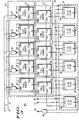
- fractional frequency divider 40 as an alternate embodiment of the present invention which eliminates the need for comparor 24.
- the high frequency input clock signal S 12 is applied at input 12
- first and second 5-bit digital signals representing integers D and N, respectively, are applied at input buses 14 and 16.
- the five conductors of input bus 16 are coupled to the first inputs of NAND gates 46, 48, 50, 52 and 54, respectively, while the outputs of NAND gates 46-54 are coupled to the INB inputs of full adders 56, 58, 60, 62 and 64.
- NAND gates 46-54 and full adders 56-64 collectively provide controllable subtracter 20.
- the Q outputs of full adders 56-64 are coupled to the INA inputs of full adders 66, 68, 70, 72 and 74, respectively, which combine to form adder 18.
- the five conductors of input bus 14 are coupled to the INB inputs of full adders 66-74, respectively.
- the carry-in of full adder 64 is coupled for receiving a logic one signal applied at input 75, while the carry-out of the same is coupled to the carry-in of full adder 62.
- the carry-out of full adder 62 is coupled to the carry-in of full adder 60, and the carry-out of full adder 60 is coupled to the carry-in of full adder 58, while the carry-out of full adder 58 is coupled to the carry-in of full adder 56.
- the carry-in of full adder 74 is coupled for receiving a logic zero signal applied at input 76, and the carry-out of adder 74 is coupled to the carry-in of full adder 72.
- the carry-out of full adder 72 is coupled to the carry-in of full adder 70, and the carry-out of full adder 70 is coupled to the carry-in of full adder 68, while the carry-out of full adder 68 is coupled to the carry-in of full adder 66.
- the Q outputs of full adders 66-74 are coupled to the D inputs of flipflops 78, 80, 82, 84 and 86, respectively, and the Q outputs of flipflops 78-86 are coupled to the INA inputs of full adders 56-64, respectively.
- the carry-out of full adder 66 is coupled to the D input of flipflop 88, and the Q output of the latter is coupled to the second inputs of NAND gates 46-54 and to the first input of AND gate 28.
- the combination of flipflops 78-88 form register 22.
- input 12 is coupled to the second input of AND gate 28, the output of which provides the output clock signal S 30 at output 30 having a frequency equal to the frequency of the input clock S 12 divided by N/D.
- Input 12 is also coupled to the CLK (clock) inputs of flipflop 78-88, while input 90 is coupled to the R (reset) input of flipflop 88 and to the S (set) inputs of flipflops 78-86.
- Flipflops 78-88 are edge-triggered D-type flipflops, wherein the digital signal applied at the D input is latched to the Q output thereof at the falling edge of input clock signal S 12 .
- the edge-triggering feature is used to avoid race conditions, i.e., when the output signal of flipflops 78-88 change state, the resulting output signal is propagated back to the inputs of the same flipflops via controllable subtracter 20 and adder 18. By using edge-triggered flipflops, it is assured that the new input signal will not propagate to the output until the following negative-going edge of input clock signal S 12 .
- fractional frequency divider 40 follows the discussion of FIG. 1 with certain distinctions as discussed below.
- the values for integers N and D are selected for an illustration of the present invention and the integers N and D may take on many different integer values provided integer N is greater than integer D.
- a reset pulse is applied at input 90 at time t 0 to load the value "011111" into register 22 which comprises flipflop 88 for the most significant bit (MSB) and flipflops 78-86 for the five least significant bits (LSB), respectively.
- Register 22 may take on other initial values such as "100000” which simply shifts the starting point of the repeating output waveform.
- the logic zero developed at the Q output of flipflop 88 is applied at the first input of AND gate 28 and to the second inputs of NAND gates 46-54 thereby producing digital signal "11111 " at the outputs thereof.
- the MSB of the 6-bit digital output signal of full adders 66-74 is provided at the carry-out of full adder 66 and applied at the D input of flipflop 88.
- input clock signal S 12 transitions to logic one and combines with the logic one at the Q output of flipflop 88 for providing logic one at output 30 during times t 2 through t 3 of FIG. 2.
- the logic one latched at the Q output of flipflop 88 also inverts the 5-bit digital signal N through NAND gates 46-54 providing "11000" at the INB inputs of full adders 56-64. Concurrently, the digital output signal of flipflops 78-86 "00001 " is applied at the INA inputs of full adders 56-64, while logic one remains at the carry-in of fuller adder 64.
- the 5-bit digital output signal of full adders 56-64 "11010” is applied at the INA inputs of full adders 66-74, while the 5-bit digital signal D "00010” is applied at the INB inputs of the same, and the 6-bit digital output signal of full adders 66-74 "011100” is clocked through to the outputs of flipflops 78-88 on the falling edge of input clock signal S 12 at time t 3 as shown in FIG. 2.
- input clock signal S 12 falls to logic zero causing output clock signal S 30 to follow.
- register 22 clocks in values "011101", "011111” and "100001" at time t 8 .
- output clock signal S 30 rises to logic one.
- the next falling edge at time t 10 returns register 22 to its value at time t 3 thereby completing two periods of output clock signal S 30 for seven cycles of input clock signal S 12 wherein the first period occurred between times t 3 and t 7 and the second period occurred between times t 7 and t 10 .
- Output clock signal S 30 cycles twice for every seven cycles of input clock signal S 12 , that is, the frequency of output clock signal S 30 is 10 MHz divided by 7/2, or approximately 2.857 MHz.
- NAND gates 46-54 are replaced with AND gates and a logic zero is applied at input 75, while the Q ⁇ output of flipflop 88 is coupled to the second inputs of AND gates 46-54.
- register 22 may be loaded with "100000" at time t 0 .
- the values latched into register 22 will be "011110" at time t 1 , "100011” at time t 3 , "100001” at time t 4 , "011111” at time t 5 , "100100” at time t 7 , and "011110” at time t 8 again returning to the value at time t 1 thereby completing the two repeating periods of output clock signal S 30 .
Landscapes
- Engineering & Computer Science (AREA)
- General Physics & Mathematics (AREA)
- Theoretical Computer Science (AREA)
- Physics & Mathematics (AREA)
- Mathematical Optimization (AREA)
- Mathematical Analysis (AREA)
- Computing Systems (AREA)
- Mathematical Physics (AREA)
- Pure & Applied Mathematics (AREA)
- General Engineering & Computer Science (AREA)
- Computational Mathematics (AREA)
- Stabilization Of Oscillater, Synchronisation, Frequency Synthesizers (AREA)
- Manipulation Of Pulses (AREA)
Claims (6)
- Schaltung, die auf ein erstes (16) und zweites (14) digitales Eingangssignal und ein Eingangstaktsignal (12) anspricht und die Frequenz des Eingangstaktsignals durch das Verhältnis des ersten und zweiten digitalen Eingangssignals teilt, umfassend:eine erste Einrichtung (20), die auf einen ersten logischen Zustand eines digitalen Steuersignals anspricht und ein erstes digitales Ausgangssignal erzeugt, das die Differenz zwischen dem ersten digitalen Eingangssignal und eine zweiten digitalen Ausgangssignal ist, wobei die erste Einrichtung auf einen zweiten logischen Zustand des digitalen Steuersignals anspricht, um das erste digitale Ausgangssignal gleich dem zweiten digitalen Ausgangssignal zu erzeugen;eine zweite Einrichtung (18, 22), die das erste digitale Ausgangssignal und das zweite digitale Eingangssignal summiert, um das zweite digitale Ausgangssignal zu erzeugen, undeine dritte Einrichtung (24), die das digitale Steuersignal aus eine Vergleich des zweiten digitalen Ausgangssignals und des ersten digitalen Eingangssignals erzeugt, wobei das digitale Steuersignal den ersten logischen Zustand aufweist, wenn das zweite digitale Ausgangssignal größer als das erste digitale Eingangssignal ist, und das digitale Steuersignal den zweiten logischen Zustand aufweist, wenn das zweite digitale Ausgangssignal kleiner als oder gleich dem ersten digitalen Eingangssignal ist.
- Schaltung nach Anspruch 1, weiter umfassend eine vierte Einrichtung (28), die auf den ersten logischen Zustand des Steuersignals und das Eingangstaktsignal anspricht und ein Ausgangstaktsignal freigibt, das bei einer Frequenz gleich der Frequenz des Eingangstaktsignals geteilt durch das Verhältnis des ersten und zweiten digitalen Eingangssignals arbeitet.
- Frequenzteilerschaltung, die auf eine erstes (16) und zweites (14) digitales Eingangssignal anspricht und ein Ausgangstaktsignal (30) erzeugt, das bei einer Frequenz arbeitet, die gleich der des Eingangstaktsignals geteilt durch das Verhältnis des ersten und zweiten digitalen Eingangssignals ist, umfassend:einen steuerbaren Addierer (56-64), der auf einen ersten logischen Zustand eines digitalen Steuersignals anspricht und ein erstes digitales Ausgangssignal erzeugt, das die Summe eines an eine erste Mehrzahl von Eingängen angelegten zweiten digitalen Ausgangssignals und des an eine zweite Mehrzahl von Eingängen angelegten ersten digitalen Eingangssignals ist, wobei der steuerbare Addierer auf einen zweiten logischen Zustand des digitalen Steuersignals anspricht, um das erste digitale Ausgangssignal gleich dem zweiten digitalen Ausgangssignal zu erzeugen;eine Subtrahiererschaltung (66-74), die geschaltet ist, die Differenz zwischen dem ersten digitalen Ausgangssignal und dem zweiten digitalen Eingangssignal zu bilden und das zweite digitale Ausgangssignal an einer Mehrzahl von Ausgängen zu erzeugen, undein Register (78-88) mit einer Mehrzahl von Eingängen, die jeweils mit der Mehrzahl von Ausgängen der Subtrahiererschaltung verbunden sind, und mit einer Mehrzahl von Ausgängen zum Speichern des zweiten digitalen Ausgangssignals, wobei die niedrigstwertigen Ausgänge der Mehrzahl von Ausgängen des Registers jeweils mit der ersten Mehrzahl von Eingängen des steuerbaren Addierers verbunden sind, und wobei der höchstwertige Ausgang der Mehrzahl von Ausgängen des Registers mit dem steuerbaren Addierer verbunden ist, um das digitale Steuersignal zu erzeugen.
- Frequenzteilerschaltung nach Anspruch 3, weiter umfassend eine Einrichtung (28), die auf den ersten logischen Zustand des digitalen Steuersignals und das Eingangstaktsignal anspricht und das Ausgangstaktsignal freigibt.
- Verfahren zum Erzeugen eines Ausgangstaktsignals, das bei einer Frequenz arbeitet, die gleich der eines Eingangstaktsignals geteilt durch das Verhältnis eines ersten und zweiten digitalen Eingangssignals ist, umfassend die Schritte:Initialisieren eines Registers, um ein erstes digitales Ausgangssignal mit einem vorbestimmten Wert bereitzustellen;Subtrahieren des ersten digitalen Eingangssignals von dein ersten digitalen Ausgangssignal, um bei Anwesenheit eines digitalen Steuersignals mit einem ersten logischen Zustand ein zweites digitales Ausgangssignal zu bilden, und andernfalls Setzen des zweiten digitalen Ausgangssignals gleich einem niedrigstwertigen Teil des ersten digitalen Eingangssignals bei Anwesenheit des digitalen Steuersignals mit einem zweiten logischen Zustand;Addieren des zweiten digitalen Ausgangssignals und des zweiten digitalen Eingangssignals, um den nächsten Wert des ersten digitalen Ausgangssignals zu erzeugen, undSpeichern des nächsten Wertes des ersten digitalen Ausgangssignals in dem Register, um den Zyklus zu wiederholen, wobei ein höchstwertiger Teil des ersten digitalen Ausgangssignals das digitale Steuersignal mit dem ersten oder zweiten logischen Zustand liefert.
- Verfahren zum Erzeugen eines Ausgangstaktsignals, das bei einer Frequenz arbeitet, die gleich der eines Eingangstaktsignals geteilt durch das Verhältnis eines ersten und zweiten digitalen Eingangssignals ist, umfassend die Schritte:Initialisieren eines Registers, um ein erstes digitales Ausgangssignal mit einem vorbestimmten Wert bereitzustellen;Subtrahieren des ersten digitalen Eingangssignals von dem ersten digitalen Ausgangssignal, um bei Anwesenheit eines digitalen Steuersignals mit einem ersten logischen Zustand ein zweites digitales Ausgangssignal zu bilden, und andernfalls Setzen des zweiten digitalen Ausgangssignals gleich einem niedrigstwertigen Teil des ersten digitalen Eingangssignals bei Anwesenheit des digitalen Steuersignals mit einem zweiten logischen Zustand;Addieren des zweiten digitalen Ausgangssignals und des zweiten digitalen Eingangssignals, um den nächsten Wert des ersten digitalen Ausgangssignals zu erzeugen;Speichern des nächsten Wertes des ersten digitalen Ausgangssignals in dem Register undVergleichen des ersten digitalen Ausgangssignals und des ersten digitalen Eingangssignals, um das digitale Steuersignal zu erzeugen, wobei das digitale Steuersignal den ersten logischen Zustand aufweist, wenn das erste digitale Ausgangssignal größer als das erste digitale Eingangssignal ist, und das digitale Steuersignal den zweiten logischen Zustand aufweist, wenn das erste digitale Ausgangssignal kleiner als oder gleich dem ersten digitalen Eingangssignal ist.
Applications Claiming Priority (2)
| Application Number | Priority Date | Filing Date | Title |
|---|---|---|---|
| US07/490,861 US5040197A (en) | 1990-03-09 | 1990-03-09 | Fractional frequency divider for providing a symmetrical output signal |
| US490861 | 1990-03-09 |
Publications (3)
| Publication Number | Publication Date |
|---|---|
| EP0445979A2 EP0445979A2 (de) | 1991-09-11 |
| EP0445979A3 EP0445979A3 (en) | 1993-02-03 |
| EP0445979B1 true EP0445979B1 (de) | 1996-06-12 |
Family
ID=23949798
Family Applications (1)
| Application Number | Title | Priority Date | Filing Date |
|---|---|---|---|
| EP91301698A Expired - Lifetime EP0445979B1 (de) | 1990-03-09 | 1991-03-01 | Frequenzteiler mit gebrochenem Teilverhältnis zur Erzeugung eines symmetrischen Ausgangssignals |
Country Status (4)
| Country | Link |
|---|---|
| US (1) | US5040197A (de) |
| EP (1) | EP0445979B1 (de) |
| JP (1) | JP3077276B2 (de) |
| DE (1) | DE69120105T2 (de) |
Families Citing this family (11)
| Publication number | Priority date | Publication date | Assignee | Title |
|---|---|---|---|---|
| US5202642A (en) * | 1991-05-09 | 1993-04-13 | Iomega Corporation | Apparatus and method for fractional frequency division |
| FR2704372B1 (fr) * | 1993-04-20 | 1995-05-24 | Commissariat Energie Atomique | Dispositif de division de fréquence. |
| US5500627A (en) * | 1994-01-19 | 1996-03-19 | Alliedsignal Inc. | Precision duty cycle phase lock loop |
| TW379293B (en) * | 1994-04-01 | 2000-01-11 | Ibm | Apparatus and method for generating a clock in a microprocessor |
| US5867068A (en) * | 1997-10-27 | 1999-02-02 | Motorola, Inc. | Frequency synthesizer using double resolution fractional frequency division |
| US6449329B1 (en) * | 2000-09-14 | 2002-09-10 | Qualcomm Incorporated | Dual-edge M/N:D counter |
| US8081017B2 (en) * | 2006-11-29 | 2011-12-20 | Nec Corporation | Clock signal frequency dividing circuit and clock signal frequency dividing method |
| US8510589B2 (en) * | 2008-08-29 | 2013-08-13 | Intel Mobile Communications GmbH | Apparatus and method using first and second clocks |
| WO2010050097A1 (ja) * | 2008-10-29 | 2010-05-06 | 日本電気株式会社 | クロック分周回路、クロック分配回路、クロック分周方法及びクロック分配方法 |
| JP6115715B2 (ja) * | 2013-03-26 | 2017-04-19 | セイコーエプソン株式会社 | クロック生成装置、電子機器、移動体及びクロック生成方法 |
| KR101682272B1 (ko) | 2014-01-27 | 2016-12-05 | 엘에스산전 주식회사 | 상승 에지 동작 시스템용 클럭 생성방법 |
Family Cites Families (5)
| Publication number | Priority date | Publication date | Assignee | Title |
|---|---|---|---|---|
| DE2032982A1 (de) * | 1970-07-03 | 1972-01-05 | Licentia Gmbh | Verfahren und Vorrichtung zur Steuerung der von einem digitalen Differenzen-Sumjnator abgegebenen Taktfrequenz |
| US3729623A (en) * | 1971-01-11 | 1973-04-24 | Gen Electric | Method for the selective multiplication and division of a pulse train and a multiply/divide circuit therefor |
| DE2849797C2 (de) * | 1978-11-16 | 1982-03-11 | Siemens AG, 1000 Berlin und 8000 München | Digitale Frequenzteileranordnung |
| SE445868B (sv) * | 1984-12-12 | 1986-07-21 | Ellemtel Utvecklings Ab | Anordning for neddelning av en klockfrekvens |
| DE3562684D1 (en) * | 1985-05-18 | 1988-06-16 | Itt Ind Gmbh Deutsche | Frequency division circuit for non-integer divisors after the manner of a rate multiplier |
-
1990
- 1990-03-09 US US07/490,861 patent/US5040197A/en not_active Expired - Lifetime
-
1991
- 1991-03-01 DE DE69120105T patent/DE69120105T2/de not_active Expired - Fee Related
- 1991-03-01 EP EP91301698A patent/EP0445979B1/de not_active Expired - Lifetime
- 1991-03-06 JP JP03194716A patent/JP3077276B2/ja not_active Expired - Fee Related
Also Published As
| Publication number | Publication date |
|---|---|
| EP0445979A3 (en) | 1993-02-03 |
| US5040197A (en) | 1991-08-13 |
| JP3077276B2 (ja) | 2000-08-14 |
| DE69120105D1 (de) | 1996-07-18 |
| DE69120105T2 (de) | 1997-01-16 |
| EP0445979A2 (de) | 1991-09-11 |
| JPH04227330A (ja) | 1992-08-17 |
Similar Documents
| Publication | Publication Date | Title |
|---|---|---|
| US6441655B1 (en) | Frequency division/multiplication with jitter minimization | |
| KR940007543B1 (ko) | 고속 프로그램가능 분주기 | |
| EP1514354B1 (de) | Digitaler delta-sigma-modulator in einem fraktional-n-frequenz-synthesizer | |
| CN110830041B (zh) | 占空比50%的连续整数分频器及包括其的锁相环电路 | |
| JP2596313B2 (ja) | 位相同期発振回路 | |
| KR100237539B1 (ko) | 주파수 합성기 | |
| EP0120702B1 (de) | Programmierbares zeitliches Ablaufsteuerungssystem | |
| JPS6243568B2 (de) | ||
| EP0800276A1 (de) | Frequenzvervielfacher, bei dem das Multiplikationsverhältnis in der ersten Stufe grösser ist als in den nachfolgenden Stufen | |
| US5088057A (en) | Rational rate frequency generator | |
| US6642800B2 (en) | Spurious-free fractional-N frequency synthesizer with multi-phase network circuit | |
| US5040197A (en) | Fractional frequency divider for providing a symmetrical output signal | |
| KR0159213B1 (ko) | 가변 지연회로 | |
| US7782988B2 (en) | Digital frequency synthesizer | |
| JP2710537B2 (ja) | クロック発生器、クロック発生方法、および標本化データ・システム | |
| US5305362A (en) | Spur reduction for multiple modulator based synthesis | |
| JPS61157022A (ja) | 周波数逓倍装置 | |
| EP0757445A2 (de) | Frequenzsynthetisierer mit einem Phasenregelkreis | |
| US5546434A (en) | Dual edge adjusting digital phase-locked loop having one-half reference clock jitter | |
| US6956922B2 (en) | Generating non-integer clock division | |
| JP3884553B2 (ja) | クロック分周器 | |
| US6108393A (en) | Enhanced prescaler phase interface | |
| US4210776A (en) | Linear digital phase lock loop | |
| US5127036A (en) | Fifty percent duty cycle divided-by-m counter | |
| JPS63151217A (ja) | 歯抜け分周回路 |
Legal Events
| Date | Code | Title | Description |
|---|---|---|---|
| PUAI | Public reference made under article 153(3) epc to a published international application that has entered the european phase |
Free format text: ORIGINAL CODE: 0009012 |
|
| AK | Designated contracting states |
Kind code of ref document: A2 Designated state(s): DE FR GB IT |
|
| PUAL | Search report despatched |
Free format text: ORIGINAL CODE: 0009013 |
|
| AK | Designated contracting states |
Kind code of ref document: A3 Designated state(s): DE FR GB IT |
|
| 17P | Request for examination filed |
Effective date: 19930715 |
|
| 17Q | First examination report despatched |
Effective date: 19950810 |
|
| GRAH | Despatch of communication of intention to grant a patent |
Free format text: ORIGINAL CODE: EPIDOS IGRA |
|
| GRAA | (expected) grant |
Free format text: ORIGINAL CODE: 0009210 |
|
| AK | Designated contracting states |
Kind code of ref document: B1 Designated state(s): DE FR GB IT |
|
| PG25 | Lapsed in a contracting state [announced via postgrant information from national office to epo] |
Ref country code: IT Free format text: LAPSE BECAUSE OF FAILURE TO SUBMIT A TRANSLATION OF THE DESCRIPTION OR TO PAY THE FEE WITHIN THE PRE;WARNING: LAPSES OF ITALIAN PATENTS WITH EFFECTIVE DATE BEFORE 2007 MAY HAVE OCCURRED AT ANY TIME BEFORE 2007. THE CORRECT EFFECTIVE DATE MAY BE DIFFERENT FROM THE ONE RECORDED.SCRIBED TIME-LIMIT Effective date: 19960612 Ref country code: FR Effective date: 19960612 |
|
| REF | Corresponds to: |
Ref document number: 69120105 Country of ref document: DE Date of ref document: 19960718 |
|
| EN | Fr: translation not filed | ||
| PLBE | No opposition filed within time limit |
Free format text: ORIGINAL CODE: 0009261 |
|
| STAA | Information on the status of an ep patent application or granted ep patent |
Free format text: STATUS: NO OPPOSITION FILED WITHIN TIME LIMIT |
|
| 26N | No opposition filed | ||
| REG | Reference to a national code |
Ref country code: GB Ref legal event code: IF02 |
|
| PGFP | Annual fee paid to national office [announced via postgrant information from national office to epo] |
Ref country code: GB Payment date: 20050207 Year of fee payment: 15 |
|
| PGFP | Annual fee paid to national office [announced via postgrant information from national office to epo] |
Ref country code: DE Payment date: 20050331 Year of fee payment: 15 |
|
| PG25 | Lapsed in a contracting state [announced via postgrant information from national office to epo] |
Ref country code: GB Free format text: LAPSE BECAUSE OF NON-PAYMENT OF DUE FEES Effective date: 20060301 |
|
| PG25 | Lapsed in a contracting state [announced via postgrant information from national office to epo] |
Ref country code: DE Free format text: LAPSE BECAUSE OF NON-PAYMENT OF DUE FEES Effective date: 20061003 |
|
| GBPC | Gb: european patent ceased through non-payment of renewal fee |
Effective date: 20060301 |