EP0446045B1 - A method of and a device for driving a wire-dot print head - Google Patents
A method of and a device for driving a wire-dot print head Download PDFInfo
- Publication number
- EP0446045B1 EP0446045B1 EP91301893A EP91301893A EP0446045B1 EP 0446045 B1 EP0446045 B1 EP 0446045B1 EP 91301893 A EP91301893 A EP 91301893A EP 91301893 A EP91301893 A EP 91301893A EP 0446045 B1 EP0446045 B1 EP 0446045B1
- Authority
- EP
- European Patent Office
- Prior art keywords
- timing signal
- drive
- drive elements
- phase
- coil
- Prior art date
- Legal status (The legal status is an assumption and is not a legal conclusion. Google has not performed a legal analysis and makes no representation as to the accuracy of the status listed.)
- Expired - Lifetime
Links
- 238000001514 detection method Methods 0.000 claims description 23
- 238000010586 diagram Methods 0.000 description 11
- BGPVFRJUHWVFKM-UHFFFAOYSA-N N1=C2C=CC=CC2=[N+]([O-])C1(CC1)CCC21N=C1C=CC=CC1=[N+]2[O-] Chemical compound N1=C2C=CC=CC2=[N+]([O-])C1(CC1)CCC21N=C1C=CC=CC1=[N+]2[O-] BGPVFRJUHWVFKM-UHFFFAOYSA-N 0.000 description 6
- 230000004907 flux Effects 0.000 description 4
- 238000010438 heat treatment Methods 0.000 description 2
- 230000004048 modification Effects 0.000 description 2
- 238000012986 modification Methods 0.000 description 2
- 238000005452 bending Methods 0.000 description 1
- 238000013021 overheating Methods 0.000 description 1
- 238000011084 recovery Methods 0.000 description 1
Images


Classifications
-
- B—PERFORMING OPERATIONS; TRANSPORTING
- B41—PRINTING; LINING MACHINES; TYPEWRITERS; STAMPS
- B41J—TYPEWRITERS; SELECTIVE PRINTING MECHANISMS, i.e. MECHANISMS PRINTING OTHERWISE THAN FROM A FORME; CORRECTION OF TYPOGRAPHICAL ERRORS
- B41J9/00—Hammer-impression mechanisms
- B41J9/44—Control for hammer-impression mechanisms
- B41J9/46—Control for hammer-impression mechanisms for deciding or adjusting hammer-firing time
-
- B—PERFORMING OPERATIONS; TRANSPORTING
- B41—PRINTING; LINING MACHINES; TYPEWRITERS; STAMPS
- B41J—TYPEWRITERS; SELECTIVE PRINTING MECHANISMS, i.e. MECHANISMS PRINTING OTHERWISE THAN FROM A FORME; CORRECTION OF TYPOGRAPHICAL ERRORS
- B41J2/00—Typewriters or selective printing mechanisms characterised by the printing or marking process for which they are designed
- B41J2/22—Typewriters or selective printing mechanisms characterised by the printing or marking process for which they are designed characterised by selective application of impact or pressure on a printing material or impression-transfer material
- B41J2/23—Typewriters or selective printing mechanisms characterised by the printing or marking process for which they are designed characterised by selective application of impact or pressure on a printing material or impression-transfer material using print wires
- B41J2/30—Control circuits for actuators
Definitions
- the present invention relates to a device for driving a wire-dot printing head
- Fig. 1 is a sectional view of a wire-dot print head of the spring charge type.
- print wires 1 extend generally parallel with each other.
- the front or forward (upper as seen in the figure) parts of the print wires 1 extend through an aperture 8a provided in the front end of a nose 8b forming the front part of a wire guide 8.
- a print medium such as print paper PP on platen PL via an ink ribbon IR thereby performing wire-dot printing.
- a plate spring 3 comprises radial parts 3a which are fixed to rear surfaces of outer or second ends of the armatures 2.
- the plate spring 3 also comprises an annular part 3b which integrally connects the outer ends of the radial parts 3a and is clamped between the front end of a cylindrical permanent magnet 4 and the rear surface of an annular part 5b of a front yoke 5.
- the front yoke 5 also comprises radial parts 5a having outer ends integrally connected by the annular part 5b.
- Each armature 2 is positioned between adjacent radial parts 5a of the front yoke 5, with a slight gap on each side.
- Cores 6 extend from a disk-shaped base yoke 10 forward and their front ends are facing the lower surfaces of the armatures 2.
- Coils 7 are wound on the cores 6 to form electromagnets EM for the respective armatures 2 and hence for the respective print wires 1.
- the rear end of the cylindrical permanent magnet 4 is connected to the periphery of the disk-shaped base yoke 10.
- the permanent magnet 4, the annular part 3b of the plate spring 3, the annular part 5b of the front yoke 5 and an annular part 8c of the wire guide 8 form a cylindrical wall of the print head.
- the magnetic flux from the permanent magnet 4 passes through the annular part 5b of the front yoke 5, the radial parts 5a of the front yoke 5, the armatures 2, the cores 6 and the base yoke 10, thereby attracting the armatures 2 toward the cores 6, bending the radial parts 3a of the plate spring 3.
- the electromagnets EM are energized to generate a magnetic flux canceling the magnetic flux from the permanent magnet 4
- the armatures 2 are released and the print wires 1 are driven forward by virtue of the recovery force of the plate spring 3.
- the period for which the electromagnets are energized is determined by a drive time signal DT 1 shown in Fig. 2.
- Another drive time signal DT 2 is used to provide, subsequent to the energization time, a period PR1 in which currents due to the electromotive forces induced in the electromagnets are allowed to flow through a certain current path. Subsequent to the first period, the currents which are also due to electromotive forces, flow through another current path for a certain period, denoted PR2, until the current falls to zero.
- PR2 an example of a wire dot print head with drive circuitry which operates in this way is described in EP-A-0 294 288.
- the wire-dot print head has a multiplicity of, e.g., 24, drive elements. They are disposed in an array or in sequence along a ring as shown in Fig. 3. In the figure, the positions of the drive elements, particularly the electromagnets on the disk-shaped base yoke 10 are illustrated. They are numbered, as #1, #2, #3, and so on, in the order in which the front ends of the corresponding print wires 1 are arranged from top to bottom. In the sequence along the circle in which the electromagnets are disposed in sequence, they are arranged in the counterclockwise direction in the order of #1, #3, #5, ... #2.
- the base yoke 10 to which the cores 9 are fixed, the permanent magnet 4, and the front yoke 5 and the like are formed as an integral unit, and for this reason much of the magnetic circuit of the drive element is shared.
- magnetic flux generated from one drive element enters a magnetic circuit of an adjacent drive element, creating a magnetic interference which brings about a variation in the magnetic circuit of the above-mentioned adjacent drive element.
- This magnetic interference not only increases the exciting current of the coil, but also gives considerable influences on the printing operation of the armatures, such as the shifting in the timing of the release of armatures.
- the variations in the armature operation due to the magnetic interference is becoming a larger problem as the speed and the printing force of the wire-dot print head are increased.
- means for detecting print data signals supplied for the respective electromagnets and the number of the electromagnets that are simultaneously driven responsive to the signals means actuated in accordance with timing signals generated every predetermined pitch of movement of wire drive element, means supplying a time signal having a length corresponding to the number of the electromagnets, and means gating the print data signals with the time signal to produce drive signals for the electromagnets are provided, and the time for which the coils are energized is thereby varied.
- the control is made based solely on the number of the coils which are energized, so the printing operations of the armatures are not necessarily constant.
- the magnetic interference gives a significant influence on the adjacent drive elements, and the degree of interference differs much depending on whether or not adjacent electromagnets are simultaneously driven.
- the time for which coils are energized is varied to minimize the influence with the combination of pins giving the worst armature operations. For this reason, with respect to the combination of the pins with which the time for which the coils are energized may be short, energy more than necessary is supplied to the coils, and the heating of the coils is increased, and the printing forces are excessive.
- a device for driving a wire dot printer having a wire dot printing head provided with wire drive elements disposed in a sequence, each wire drive element including an electrically energizable coil and switching means for controlling current flow through the coil, the device comprising means for controlling the energization of the respective drive elements cyclically for respective energization periods in accordance with print data for the respective drive elements, the print data being indicative of whether or not the respective wire drive elements are to be driven for each cycle, each said energization period including a first phase during which energy is supplied to the coil, followed by a second phase during which said supply of energy is removed and current flow through the coil is maintained by self inductance, and a third phase during which a sink is provided for the self-induced current, the second phases for all the drive elements terminating at a fixed time and at substantially the same time for a given cycle, timing signal generating means for generating first and second timing signal configurations that define durations for said first and said second phases of each
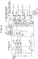
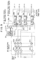
- Fig. 4 is a circuit diagram showing a print head drive control circuit of an embodiment of the invention.
- Print data #1, #3, #5, ..., #2 are supplied, each print cycle, from a print data generating unit, not shown, for respective drive elements and hence for respective print wires 1 and determine whether the corresponding print wires 1 are to be driven during the particular print cycle.
- Identical reference marks #1, #3, #5, ..., #2 are used to correlate the print data with the drive elements for which the print data are generated.
- the print data are input to a detecting circuit 20 as well as to drive circuits later described.
- the detecting circuit 20 detects, for each drive element, whether said each drive element and at least one of the drive elements adjacent to the first-mentioned drive element are to be energized in the particular print cycle. This detection is made in accordance with the print data #1, #3, #5, ..., #2. The results of the detection are detection signals 20a, 20b, 20c, ..., 20x.
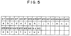
- the alphabetical suffixes a, b, c, ..., x respectively correspond to #1, #3, #5, ..., #2 of the drive elements.
- Fig. 5 shows the correspondence between the number (#) of each of drive elements and the alphabetical suffixes of each detection signal.
- the detecting circuit 20 comprises logical product circuit (hereinafter referred to as AND gates) 21a, 21b, 21c, ..., 21x, and logical sum circuits (hereinafter referred to as OR gates) 22a, 22b, 22c, ..., 22x.
- the AND gates 21a receives print data #1 and #3.
- the AND gate 21b receives print data #3 and #5.
- the AND gate 21c receives print data #5 and #7.
- the last AND gate 21x receives print data #1 and #2. That is, two print data which are for drive elements adjacent to each other in the circular sequence in which they are disposed as shown in Fig. 3 are applied to inputs of each of the AND gates 21a, 21b, 21c, ..., 21x.
- the OR gate 22a receives the output signals from the AND gates 21a and 21x.
- the OR gate 22b receives the output signals from the AND gates 21a and 21b.
- the OR gate 22c receives the output signals from the AND gates 21b and 21c. That is, the OR gates 22b to 22x receive the output signals of pairs of AND gates 21a to 21x in the front stage that are adjacent to each other.
- the OR gate 22a receives the output signals of the AND gate 21a of the uppermost position and the AND gate 21x of the lowermost position.
- the AND gates of each of said pairs receive one common print data for a certain drive element, and two print data which are for drive elements adjacent, on both respective sides, to said certain drive element.
- Each of the AND gates 21a, 21b, 21c, ..., 21x detects whether the print data for each drive element and the drive element next (in the order of arrangement) to the first-mentioned drive element are both active meaning that these two drive elements are to be energized in the particular print cycle.
- Each of the OR gates 22a, 22b, 22c, ..., 22x detects whether the print data for the corresponding drive element and at least one of the drive elements adjacent to the first-mentioned drive element are both active.
- the detecting circuit 20 finds, on the basis of the input print data, that the print data for the corresponding drive element as well as one or both of the print data for the drive elements adjacent to the first-mentioned drive element in question are both at "1", it generates the detection signal of "1" for the particular drive elements. Otherwise, it generates the detection signal of "0" for the particular print data.
- the timing signal generating circuit 23 generates an on-timing signal ST, and off-timing signals STP 1 , STP 2 in time with the generation of the print data. Responsive to the on-timing signal ST, the drive time signals DT 1-1 , DT 1-3 , DT 1-5 , ..., DT 1-2 for the respective drive elements are turned on. Responsive to the off-timing signals STP 1 , STP 2 , the drive time signals DT 1-1 , DT 1-3 , DT 1-5 , ..., DT 1-2 for the respective drive elements are turned off. The drive time signal DT 2 is also generated, with its on-timing (leading edge) and off-timing (trailing edge) being coincident with that in the prior art.
- the off-timing signal selecting circuit 24 comprises data selectors 24a, 24b, 24c, ..., 24x, which receive, at the input terminals A and B, the off-timing signals STP 1 and STP 2 generated by the timing signal generating circuit 23.
- Each of the data selectors receives, at its data select terminal S, the corresponding detection signal from the detecting circuit 20, and when the signal at terminal S is at "1" it selects the signal being input to terminal A and output the selected signal through the output terminal Y.
- the data selector selects the signal being input at terminal B and output the selected signal through the output terminal Y.
- the drive time signal generating circuit 25 comprises JK flip-flops 25a, 25b, 25c, ..., 25x.
- Input to the J terminal of each JK flip-flop is the on-timing signal ST generated by the timing signal generating circuit 23.
- Input to the K terminal of each JK flip-flop is the output of the corresponding data selector of the off-timing signal selecting circuit 24.
- Input to the reset terminals R of the JK flip-flops 25a, 25b, 25c, ..., 25x are print data #1, #3, #5, ..., #2.
- the output signals DT 1-1 , DT 1-3 , DT 1-5 , ..., DT 1-2 of the JK flip-flops are the drive time signals for controlling the coil currents through the drive elements #1, #3, #5, ..., #2, and are used in place of the drive time signal DT 1 in the prior art.
- the drive time signal for each drive element of which an adjacent drive element is driven is turned on responsive to the on-timing signal ST and is turned off responsive to the off-timing signal STP 1 .
- the drive time signals for other drive elements are turned on responsive to the on-timing signal ST and are turned off responsive to the off-timing signal STP 2 .
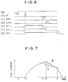
- Fig. 6 is a time chart of the print head drive control circuit in Fig. 4.
- Fig. 6 shows, at (a), the print data #1, #3, #5, ...., #2.
- Fig. 6 shows, at (b), (c) and (d), respectively show the on-timing signal ST, and the off-timing signals STP 1 and STP 2 generated by the timing signal generating circuit 23.
- Fig. 6 shows, at (e), the drive time signal DT 1-n which is turned on and off responsive to the on-timing signal ST and the off-timing signal STP 1 .
- Fig. 6 shows, at (f), the drive time signal DT 1-n′ which is turned on and off responsive to the on-timing signal ST and the off-timing signal STP 2 .
- the suffixes "n" and "n′” correspond to the numbers of the drive elements.
- Fig. 6 shows, at (g), the drive time signal DT 2 .
- Fig. 7 shows waveforms of the coil currents corresponding to Fig. 6.
- the waveform A is obtained when the drive time signal DT 1-n is used, while the waveform B is obtained when the drive time signal DT 1-n′ is used.
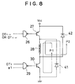
- Fig. 8 shows part of the drive circuit for a single drive element.
- the drive time signal DT 1-n or DT 1-n′ is inverted at the inverter 26, and is input to the base of a PNP transistor 27.
- the drive time signal DT 2 is input to an AND gate 29 together with print data, and their logical product is determined, and input to the base of an NPN transistor 30.
- Connected to the collector of the transistor 27 is a first end of a coil 28.
- Connected to the collector of the transistor 30 is a second end of the coil 28.
- Connected to the emitter of the transistor 27 is a power supply Vcc, and the emitter of the transistor 30 is connected to the ground.
- a diode 41 is connected across the series connection of the coil 28 and the transistor 30, with its anode connected to the emitter of the transistor 30 and its cathode connected to the first end of the coil 28.
- Another diode 42 is connected across the series connection of the transistor 27 and the coil 28, with its anode connected to the second end of the coil 28 and with its cathode connected to the emitter of the transistor 27.
- a circuit similar to that shown in Fig. 8 is provided for each of the drive elements.
- the detection signals 20c, 20d, 24e, 24s and 24t corresponding to the drive elements #5, #7, #9, #10, and #12 will assume level “1" and other detection signals will assume level "0".
- the data selectors 24c, 24d, 24e, 24s and 24t of the off-timing signal selection means 24 select the off-timing signals STP 1 and supply it to the drive time signal generating circuit 25.
- Other data selectors select the off-timing signal STP 2 , and supply it to the drive time signal generating circuit 25.
- the on-timing signal ST rises to level "1".
- the JK flip-flops of the drive time signal generating circuit 25 operate in accordance with clock pulses not shown and the drive time signals DT 1-1 , DT 1-3 , DT 1-5 , ...DT 1-2 rise to level "1".
- the drive time signals DT 1-5 , DT 1-7 , DT 1-9 , DT 1-10 , and DT 1-12 rise and fall at the timings T 2 and T 3 , like the drive time signal DT 1-n shown in Fig. 6 at (e), and other drive time signals rise and fall at T 2 and T 4 like the drive time signal DT 1-n′ shown in Fig. 6 at (f).
- the drive time signal DT 2 then will also be at level "1".
- the drive time signals DT 1-1 , DT 1-3 , DT 1-5 , ..., DT 1-2 and the drive time signals DT 2 are supplied to the drive circuits of the respective drive elements, like that shown in Fig. 8, and determine, together with the print data for each drive element, whether to energize the coil and when to start and stop the energization.
- the print data for the coils #5, #7, #9, #10, #12, #15 and #20 are "1" and other print data are at "0".
- the energization of these coils is commenced at T 2 .
- the detection signals for the coils #5, #7, #9, #10, and #12 are at "1", so the energization of the corresponding coils is terminated at T 3 .
- the detection signals for the coils #15 and #20 are at "0", so the energization of the corresponding coils is terminated at T 4 .
- the "energization” as used here means turning on both the transistors 27 and 30 for supplying a current from the power supply Vcc, through the coil and to the ground.
- the transistor 27 is turned off, but the transistor 30 is kept on.
- a current continues to flow through a path P1 consisting of the coil 28, the transistor 30 and the diode 41.
- the current gradually falls as indicated by curves A and B in Fig. 7.
- the curve A is for the case in which the energization is terminated at T 3
- the curve B is for the case in which the energization is terminated at T 4 .
- the transistor 28 is thereafter turned off, at the trailing edge of the drive time signal DT 2 .
- the current due to the electromotive force then begins to flow from the ground, through a path P2 consisting of the diode 41, the coil 28, and the diode 42, to the power supply Vcc.
- the current through the path P2 rapidly falls, as shown in Fig. 7.
- the trailing edges of the drive time signals DT 1-1 , DT 1-3 , DT 1-5 , ..., DT 1-2 are controlled in accordance with detection signals indicating whether or not an adjacent drive element is driven. Accordingly, the coil energization time for the drive element which is adjacent can be made shorter than the coil energization time which is not adjacent.
- Fig. 9 is a circuit diagram showing a drive control circuit for the print head of a second embodiment of the invention.
- the difference from the first embodiment is that the leading edges of the drive time signals rather than the trailing edges are controlled for the purpose of varying the lengths of the energization times.
- the timing signal generating circuit 31, the on-timing signal selecting circuit 32 and the drive time signal generating circuit 33 have different configurations.
- the timing signal generating circuit 31 generates first and second on-timing signals ST 1 and ST 2 for turning on the drive time signals DT 1-1 , DT 1-3 , DT 1-5 , ..., DT 1-2 , and a single off-timing signal STP for turning off the drive time signals DT 1-1 , DT 1-3 , DT 1-5 , ..., DT 1-2 , in time with the generation of the print data.
- the drive time signal DT 2 is also generated.
- the on-timing signal selecting circuit 32 comprises data selectors 32a, 32b, 32c, ..., 32x, which receive at the data input terminals A and B the on-timing signals ST 1 and ST 2 generated by the timing signal generating circuit 31. They receive, at the data select terminals S, the detection signals from the detecting circuit 20, and responsive to the detection signal of "1" they select the signal being input to the terminal B and output it to the output terminal Y, and responsive to the detection signal of "0” they select the signal input to the terminal A and output it the output terminal Y.
- the drive time signal generating circuit 33 comprises JK flip-flops 33a, 33b, 33c, ..., 33x.
- Input to the J terminal of each JK flip-flop are the output signals from the respective data selectors.
- Input to the K terminal of each JK flip-flop is the off-timing signal STP generated by the timing signal generating circuit 31.
- Input to the reset terminals R of the JK flip-flops 33a, 33b, 33c, ..., 33x are print data #1, #3, #5, ..., #2.
- the output signals DT 1-1 , DT 1-3 , DT 1-5 , ..., DT 1-2 of the JK flip-flops are the drive time signals for controlling the energization of the corresponding drive elements #1, #3, #5, ..., #2, and are used in place of the drive time signal DT 1 mentioned in the description of the prior art.
- the drive time signal for each drive element of which an adjacent drive element is driven is turned on responsive to the on-timing signal ST 2 , and is turned off with the off-timing signal STP.
- the drive time signals for other drive elements are turned on with the on-timing signal ST 1 and is turned off with the off-timing signal STP.
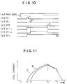
- Fig. 10 is a time chart of the print head drive control circuit in Fig. 9.
- Fig. 10 shows, at (a), the print data #1, #3, #5, ...., #2.
- Fig. 10 shows, at (b), (c) and (d), the on-timing signals ST 1 , ST 2 , and the off-timing signal STP generated by the timing signal generating circuit 31.
- Fig. 10 shows, at (e), the drive time signal DT 1-n which is turned on and off with the on-timing signal ST 1 and the off-timing signal STP.
- Fig. 10 shows, at (f), the drive time signal DT 1-n′ which is turned on and off with the on-timing signal ST 2 and the off-timing signal STP.
- the suffixes "n" and "n′” correspond to the numbers of the drive elements.
- Fig. 10 shows, at (g), the drive time signal DT 2 .
- the drive time signals DT 1-n , DT 1-n′ and DT 2 as well as the print data are input to the drive circuits of the drive elements to determine whether and when to energize the respective drive elements.
- Fig. 11 shows waveforms of the coil currents corresponding to Fig. 10.
- the waveform C is for the drive time signal DT 1-n and is obtained when the energization is commenced at T 2 .
- the waveform D is for the drive time signal DT 1-n′ and is obtained when the energization is commenced at T 3 .
- the operation will now be described. As an example, it is assumed that the drive elements #5, #7, #9, #10, #12, #15 and #20 are driven, as in the first embodiment.
- the print data #1, #3, #5, ..., #2 are input at time T 1 shown in Fig. 9, to the detecting circuit 20 shown in Fig. 9.
- the print data for the drive elements #5, #7, #9, #10, #12, #15 and #20 are at "1".
- the drive elements #5, #7, #9, #10 and #12 have their neighboring drive elements simultaneously driven, so the detection signals corresponding to the drive elements #5, #7, #9, #10, and #12 will assume level "1" and other detection signals will assume level "0".
- the data selectors 32c, 32d, 32e, 32s and 32t of the on-timing signal selection means 32 select the on-timing signals ST 2 and supply it to the drive time signal generating circuit 33.
- Other data selectors select the on-timing signal ST 1 , and supply it to the drive time signal generating circuit 33.
- the on-timing signal ST 1 rises to level "1", responsive to which the drive time signal DT 1-n corresponding to the drive elements other than the drive elements #5, #7, #9, #10 and #12 rise to level "1".
- the on-timing signal ST 2 rises to level "1", responsive to which the drive time signals DT 1-n′ corresponding to the drive elements #5, #7, #9, #10 and #12 rise to level "1".
- Input to the drive circuits of the drive elements #15 and #20 are the drive time signals DT 1-n , DT 2 and the print data #15 and #20, and the drive elements are energized so as to conduct a current as indicated by waveform C in Fig. 11.
- Input to the drive circuits of the drive elements #5, #7, #9, #10 and #12 are the drive time signals DT 1-n′ , DT 2 and the print data #5, #7, #9, #10 and #12, and the drive elements are energized so as to conduct a current as indicated by waveform D shown in Fig. 11.
- the off-timing signal STP rises to "1", responsive to which the the JK flip-flops of the drive time signal generating circuit 33 shown in Fig. 9 operate, in accordance with clock pulses not shown, to set the drive time signals DT 1-n and DT 1-n′ to "0".
- the energization of the drive elements #5, #7, #9, #10, #12, #15 and #20 (the current supply to the coils of the drive elements #5, #7, #9, #10, #12, #15 and #20 from the power supply Vcc) is terminated.
- the drive time signal DT 2 falls to level "0". The attenuation of the coil current due to the electromotive force rapidly falls as illustrated.
- the detecting circuit 20 detects, for each drive element, whether said each drive element and at least one of the drive elements adjacent to the first-mentioned drive element are to be energized in the particular print cycle
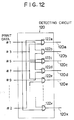
- the detecting circuit 20 may alternatively be so arranged to detect, for each of the drive elements, whether at least one of the drive elements adjacent to the first-mentioned drive element is driven during each print cycle.
- This can be implemented by a detecting circuit 120 shown in Fig. 12. It comprises OR gates 122a to 122x for the respective drive elements.
- Each OR gate for each drive element is connected to receive the print data for the drive elements adjacent to the drive element in question and using the output of the OR gate as the detection signal 120a to 120x. Using such detection signals will produce the same results since the drive elements are not actually energized unless the corresponding print data input to the AND gate 29 at the base of the driving transistor 30 is also active.
- the energization time for each drive element is determined depending on whether or not an adjacent drive element is simultaneously energized: it is shortened if the adjacent drive element is also energized. Accordingly, supply of excessive energy to drive elements whose neighbouring adjacent drive element is driven simultaneously is avoided, and the heating of the wire-dot print head is reduced, the print quality can be made uniform, and a high-speed wire-dot print head having a desirable armature operation can be provided.
Landscapes
- Dot-Matrix Printers And Others (AREA)
Description
- The present invention relates to a device for driving a wire-dot printing head
- Hitherto, various types of wire-dot print heads have been used for a wire-dot printers. Spring-charged wire-dot print heads are widely used in applications where high speeds and high printing forces are desired. Fig. 1 is a sectional view of a wire-dot print head of the spring charge type.
- In the figure,
print wires 1 extend generally parallel with each other. The front or forward (upper as seen in the figure) parts of theprint wires 1 extend through anaperture 8a provided in the front end of anose 8b forming the front part of awire guide 8. When theprint wires 1 are driven forward, in a manner later described, their front ends strike a print medium, such as print paper PP on platen PL via an ink ribbon IR thereby performing wire-dot printing. - Rear (lower as seen in the figure) ends of the
print wires 1 are fixed to inner or first ends ofarmatures 2 which are disposed to extend radially. Aplate spring 3 comprisesradial parts 3a which are fixed to rear surfaces of outer or second ends of thearmatures 2. Theplate spring 3 also comprises anannular part 3b which integrally connects the outer ends of theradial parts 3a and is clamped between the front end of a cylindricalpermanent magnet 4 and the rear surface of an annular part 5b of afront yoke 5. - The
front yoke 5 also comprisesradial parts 5a having outer ends integrally connected by the annular part 5b. Eacharmature 2 is positioned between adjacentradial parts 5a of thefront yoke 5, with a slight gap on each side. Cores 6 extend from a disk-shaped base yoke 10 forward and their front ends are facing the lower surfaces of thearmatures 2.Coils 7 are wound on the cores 6 to form electromagnets EM for therespective armatures 2 and hence for therespective print wires 1. The rear end of the cylindricalpermanent magnet 4 is connected to the periphery of the disk-shaped base yoke 10. Thepermanent magnet 4, theannular part 3b of theplate spring 3, the annular part 5b of thefront yoke 5 and anannular part 8c of thewire guide 8 form a cylindrical wall of the print head. - The magnetic flux from the
permanent magnet 4 passes through the annular part 5b of thefront yoke 5, theradial parts 5a of thefront yoke 5, thearmatures 2, the cores 6 and thebase yoke 10, thereby attracting thearmatures 2 toward the cores 6, bending theradial parts 3a of theplate spring 3. When the electromagnets EM are energized to generate a magnetic flux canceling the magnetic flux from thepermanent magnet 4, thearmatures 2 are released and theprint wires 1 are driven forward by virtue of the recovery force of theplate spring 3. - Further details of this action are described in for example Japanese Patent Kokai Publication No. 53860/1989. The period for which the electromagnets are energized is determined by a drive time signal DT1 shown in Fig. 2. Another drive time signal DT2 is used to provide, subsequent to the energization time, a period PR1 in which currents due to the electromotive forces induced in the electromagnets are allowed to flow through a certain current path. Subsequent to the first period, the currents which are also due to electromotive forces, flow through another current path for a certain period, denoted PR2, until the current falls to zero. An example of a wire dot print head with drive circuitry which operates in this way is described in EP-A-0 294 288.
- An assembly, particularly the electromagnet EM, for driving a single print wire will be called a wire drive element. The wire-dot print head has a multiplicity of, e.g., 24, drive elements. They are disposed in an array or in sequence along a ring as shown in Fig. 3. In the figure, the positions of the drive elements, particularly the electromagnets on the disk-
shaped base yoke 10 are illustrated. They are numbered, as #1, #2, #3, and so on, in the order in which the front ends of thecorresponding print wires 1 are arranged from top to bottom. In the sequence along the circle in which the electromagnets are disposed in sequence, they are arranged in the counterclockwise direction in the order of #1, #3, #5, ... #2. - For the purpose of reducing the size and cost of the wire-dot print head, the
base yoke 10 to which thecores 9 are fixed, thepermanent magnet 4, and thefront yoke 5 and the like are formed as an integral unit, and for this reason much of the magnetic circuit of the drive element is shared. As a result, magnetic flux generated from one drive element enters a magnetic circuit of an adjacent drive element, creating a magnetic interference which brings about a variation in the magnetic circuit of the above-mentioned adjacent drive element. This magnetic interference not only increases the exciting current of the coil, but also gives considerable influences on the printing operation of the armatures, such as the shifting in the timing of the release of armatures. The variations in the armature operation due to the magnetic interference is becoming a larger problem as the speed and the printing force of the wire-dot print head are increased. - Systems have been proposed in which the time for which currents are made to flow through the coils, i.e., the time for which the coils are energized are varied, depending on the number of the coils that are simultaneously excited, and these systems are used as effective means. One of such systems is disclosed in Japanese Patent Kokoku Publication No. 30154/1988. According to this publication, means for detecting print data signals supplied for the respective electromagnets and the number of the electromagnets that are simultaneously driven responsive to the signals, means actuated in accordance with timing signals generated every predetermined pitch of movement of wire drive element, means supplying a time signal having a length corresponding to the number of the electromagnets, and means gating the print data signals with the time signal to produce drive signals for the electromagnets are provided, and the time for which the coils are energized is thereby varied.
- In the conventional wire-dot printers, the control is made based solely on the number of the coils which are energized, so the printing operations of the armatures are not necessarily constant. For instance, the magnetic interference gives a significant influence on the adjacent drive elements, and the degree of interference differs much depending on whether or not adjacent electromagnets are simultaneously driven. Usually, the time for which coils are energized is varied to minimize the influence with the combination of pins giving the worst armature operations. For this reason, with respect to the combination of the pins with which the time for which the coils are energized may be short, energy more than necessary is supplied to the coils, and the heating of the coils is increased, and the printing forces are excessive.
- An explanation will now be given of the influence on the armature operations both in a situation in which adjacent drive elements are simultaneously driven and a situation in which adjacent drive elements are not simultaneously driven. As described earlier, the magnetic interference gives the largest influence on an adjacent drive element, and the more separated the driven elements are, the smaller is the influence. The influence appears as the variation in the inductance of the magnetic circuit of the drive element, and the phenomena vary depending on the number and positions of elements that are simultaneously driven. The phenomena also vary depending on the structure and the material of the wire-dot print head. It is therefore difficult to determine whether the magnetic interference accelerates or retards the operation of the armatures.
- It is known that for a different type of printing head the energisation of adjacent print elements can require the energisation levels of the elements to be increased, as described in JP-A-64 53 860.
- In accordance with the present invention there is provided a device for driving a wire dot printer having a wire dot printing head provided with wire drive elements disposed in a sequence, each wire drive element including an electrically energizable coil and switching means for controlling current flow through the coil, the device comprising means for controlling the energization of the respective drive elements cyclically for respective energization periods in accordance with print data for the respective drive elements, the print data being indicative of whether or not the respective wire drive elements are to be driven for each cycle, each said energization period including a first phase during which energy is supplied to the coil, followed by a second phase during which said supply of energy is removed and current flow through the coil is maintained by self inductance, and a third phase during which a sink is provided for the self-induced current, the second phases for all the drive elements terminating at a fixed time and at substantially the same time for a given cycle, timing signal generating means for generating first and second timing signal configurations that define durations for said first and said second phases of each energization period and drive circuit means responsive to the individual timing signal configurations for driving the individual drive elements characterised by logic gate means responsive to said print data, for producing individual detection signals for the respective drive elements, representative of whether an adjacent drive element is to be concurrently energized and selecting means responsive to the individual detection signals for selecting said first or second timing signal configurations for each of the drive elements individually, said drive circuit means being responsive to the individual timing signal configurations selected by the selecting means for the respective drive elements, for driving the individual drive elements such that the first phase of the respective energization period assumes said relatively short duration when an adjacent drive element is to be concurrently energized.
- By means of the invention, overheating of the printing head can be avoided.
- The invention will now be described by way of example, reference being had to the accompanying drawings, in which:
- FIGURE 1 is a sectional view of a typical known print head;
- FIGURE 2 is a waveform diagram for the known drive circuit;
- FIGURE 3 is a diagram showing the arrangement of the drive elements;
- FIGURE 4 is a diagram showing a drive control circuit for a print head driving device, in accordance with the invention;
- FIGURE 5 is a diagram showing the arrangement of the drive elements on the base yoke;
- FIGURE 6 is a time chart of the drive control circuit for the print head;
- FIGURE 7 is a waveform diagram of the coil current corresponding to Figure 6;
- FIGURE 8 is a circuit diagram showing part of the drive circuit;
- FIGURE 9 is a block diagram showing the drive control circuit for a print head driving device for a second embodiment of the invention;
- FIGURE 10 is a time chart of the drive circuit for the print head shown in Figure 9;
- FIGURE 11 is a waveform diagram of the coil currents corresponding to Figure 10; and
- FIGURE 12 is a circuit diagram showing a modification of a detecting circuit.
- In the drawings, identical elements throughout various figures are denoted by identical reference marks.
- Fig. 4 is a circuit diagram showing a print head drive control circuit of an embodiment of the invention. Print
data # 1, #3, #5, ..., #2 are supplied, each print cycle, from a print data generating unit, not shown, for respective drive elements and hence forrespective print wires 1 and determine whether thecorresponding print wires 1 are to be driven during the particular print cycle. Identicalreference marks # 1, #3, #5, ..., #2 are used to correlate the print data with the drive elements for which the print data are generated. - The print data are input to a detecting
circuit 20 as well as to drive circuits later described. - The detecting
circuit 20 detects, for each drive element, whether said each drive element and at least one of the drive elements adjacent to the first-mentioned drive element are to be energized in the particular print cycle. This detection is made in accordance with theprint data # 1, #3, #5, ..., #2. The results of the detection aredetection signals - The detecting
circuit 20 comprises logical product circuit (hereinafter referred to as AND gates) 21a, 21b, 21c, ..., 21x, and logical sum circuits (hereinafter referred to as OR gates) 22a, 22b, 22c, ..., 22x. The ANDgates 21a receivesprint data # 1 and #3. The ANDgate 21b receivesprint data # 3 and #5. The ANDgate 21c receivesprint data # 5 and #7. The last ANDgate 21x receivesprint data # 1 and #2. That is, two print data which are for drive elements adjacent to each other in the circular sequence in which they are disposed as shown in Fig. 3 are applied to inputs of each of the ANDgates - The
OR gate 22a receives the output signals from the ANDgates gate 22b receives the output signals from the ANDgates OR gate 22c receives the output signals from the ANDgates gates 22b to 22x receive the output signals of pairs of ANDgates 21a to 21x in the front stage that are adjacent to each other. TheOR gate 22a receives the output signals of the ANDgate 21a of the uppermost position and the ANDgate 21x of the lowermost position. Thus, the AND gates of each of said pairs receive one common print data for a certain drive element, and two print data which are for drive elements adjacent, on both respective sides, to said certain drive element. - Each of the AND
gates - Each of the
OR gates - When the detecting
circuit 20 finds, on the basis of the input print data, that the print data for the corresponding drive element as well as one or both of the print data for the drive elements adjacent to the first-mentioned drive element in question are both at "1", it generates the detection signal of "1" for the particular drive elements. Otherwise, it generates the detection signal of "0" for the particular print data. - The timing
signal generating circuit 23 generates an on-timing signal ST, and off-timing signals STP1, STP2 in time with the generation of the print data. Responsive to the on-timing signal ST, the drive time signals DT1-1, DT1-3, DT1-5, ..., DT1-2 for the respective drive elements are turned on. Responsive to the off-timing signals STP1, STP2, the drive time signals DT1-1, DT1-3, DT1-5, ..., DT1-2 for the respective drive elements are turned off. The drive time signal DT2 is also generated, with its on-timing (leading edge) and off-timing (trailing edge) being coincident with that in the prior art. - The off-timing
signal selecting circuit 24 comprisesdata selectors 24a, 24b, 24c, ..., 24x, which receive, at the input terminals A and B, the off-timing signals STP1 and STP2 generated by the timingsignal generating circuit 23. Each of the data selectors receives, at its data select terminal S, the corresponding detection signal from the detectingcircuit 20, and when the signal at terminal S is at "1" it selects the signal being input to terminal A and output the selected signal through the output terminal Y. When the signal at the select terminal S at "0" the data selector selects the signal being input at terminal B and output the selected signal through the output terminal Y. - The drive time
signal generating circuit 25 comprises JK flip-flops signal generating circuit 23. Input to the K terminal of each JK flip-flop is the output of the corresponding data selector of the off-timingsignal selecting circuit 24. Input to the reset terminals R of the JK flip-flops print data # 1, #3, #5, ..., #2. The output signals DT1-1, DT1-3, DT1-5, ..., DT1-2 of the JK flip-flops are the drive time signals for controlling the coil currents through thedrive elements # 1, #3, #5, ..., #2, and are used in place of the drive time signal DT1 in the prior art. The drive time signal for each drive element of which an adjacent drive element is driven is turned on responsive to the on-timing signal ST and is turned off responsive to the off-timing signal STP1. The drive time signals for other drive elements are turned on responsive to the on-timing signal ST and are turned off responsive to the off-timing signal STP2. - Fig. 6 is a time chart of the print head drive control circuit in Fig. 4. Fig. 6 shows, at (a), the
print data # 1, #3, #5, ...., #2. Fig. 6 shows, at (b), (c) and (d), respectively show the on-timing signal ST, and the off-timing signals STP1 and STP2 generated by the timingsignal generating circuit 23. Fig. 6 shows, at (e), the drive time signal DT1-n which is turned on and off responsive to the on-timing signal ST and the off-timing signal STP1. Fig. 6 shows, at (f), the drive time signal DT1-n′ which is turned on and off responsive to the on-timing signal ST and the off-timing signal STP2. In the reference marks, the suffixes "n" and "n′" correspond to the numbers of the drive elements. Fig. 6 shows, at (g), the drive time signal DT2. - Fig. 7 shows waveforms of the coil currents corresponding to Fig. 6. The waveform A is obtained when the drive time signal DT1-n is used, while the waveform B is obtained when the drive time signal DT1-n′ is used.
- Fig. 8 shows part of the drive circuit for a single drive element. The drive time signal DT1-n or DT1-n′ is inverted at the
inverter 26, and is input to the base of aPNP transistor 27. The drive time signal DT2 is input to an ANDgate 29 together with print data, and their logical product is determined, and input to the base of anNPN transistor 30. Connected to the collector of thetransistor 27 is a first end of acoil 28. Connected to the collector of thetransistor 30 is a second end of thecoil 28. Connected to the emitter of thetransistor 27 is a power supply Vcc, and the emitter of thetransistor 30 is connected to the ground. Adiode 41 is connected across the series connection of thecoil 28 and thetransistor 30, with its anode connected to the emitter of thetransistor 30 and its cathode connected to the first end of thecoil 28. Anotherdiode 42 is connected across the series connection of thetransistor 27 and thecoil 28, with its anode connected to the second end of thecoil 28 and with its cathode connected to the emitter of thetransistor 27. A circuit similar to that shown in Fig. 8 is provided for each of the drive elements. - The operation will now be described. As an example, it is assumed that the drive elements represented by black dots in the sequence of drive elements shown in Fig. 3, #5, #7, #9, #10, #12, #15 and #20 are to be driven, and the drive elements represented by white dots are not to be driven. This means, the
drive elements # 5, #7, #9, #10, and #12 and least one of their neighboring drive elements are simultaneously driven, while the drive elements adjacent to thedrive elements # 15 and #20 are not driven. Theprint data # 1, #3, #5, ..., #2 are input at time T1 shown in Fig. 6, to the detectingcircuit 20 shown in Fig. 4. The detection signals 20c, 20d, 24e, 24s and 24t corresponding to thedrive elements # 5, #7, #9, #10, and #12 will assume level "1" and other detection signals will assume level "0". As a result, the data selectors 24c, 24d, 24e, 24s and 24t of the off-timing signal selection means 24 select the off-timing signals STP1 and supply it to the drive timesignal generating circuit 25. Other data selectors select the off-timing signal STP2, and supply it to the drive timesignal generating circuit 25. - At time T2, the on-timing signal ST rises to level "1". The JK flip-flops of the drive time
signal generating circuit 25 operate in accordance with clock pulses not shown and the drive time signals DT1-1, DT1-3, DT1-5, ...DT1-2 rise to level "1". The drive time signals DT1-5, DT1-7, DT1-9, DT1-10, and DT1-12 rise and fall at the timings T2 and T3, like the drive time signal DT1-n shown in Fig. 6 at (e), and other drive time signals rise and fall at T2 and T4 like the drive time signal DT1-n′ shown in Fig. 6 at (f). The drive time signal DT2 then will also be at level "1". The drive time signals DT1-1, DT1-3, DT1-5, ..., DT1-2 and the drive time signals DT2 are supplied to the drive circuits of the respective drive elements, like that shown in Fig. 8, and determine, together with the print data for each drive element, whether to energize the coil and when to start and stop the energization. - In the example under consideration, the print data for the
coils # 5, #7, #9, #10, #12, #15 and #20 are "1" and other print data are at "0". The energization of these coils is commenced at T2. The detection signals for thecoils # 5, #7, #9, #10, and #12 are at "1", so the energization of the corresponding coils is terminated at T3. On the other hand, the detection signals for thecoils # 15 and #20 are at "0", so the energization of the corresponding coils is terminated at T4. - The "energization" as used here means turning on both the
transistors transistor 27 is turned off, but thetransistor 30 is kept on. Then, due to the electromotive force induced in thecoil 28, a current continues to flow through a path P1 consisting of thecoil 28, thetransistor 30 and thediode 41. The current gradually falls as indicated by curves A and B in Fig. 7. The curve A is for the case in which the energization is terminated at T3, while the curve B is for the case in which the energization is terminated at T4. Thetransistor 28 is thereafter turned off, at the trailing edge of the drive time signal DT2. The current due to the electromotive force then begins to flow from the ground, through a path P2 consisting of thediode 41, thecoil 28, and thediode 42, to the power supply Vcc. The current through the path P2 rapidly falls, as shown in Fig. 7. - As has been described according to the above embodiment, the trailing edges of the drive time signals DT1-1, DT1-3, DT1-5, ..., DT1-2 are controlled in accordance with detection signals indicating whether or not an adjacent drive element is driven. Accordingly, the coil energization time for the drive element which is adjacent can be made shorter than the coil energization time which is not adjacent.
- Fig. 9 is a circuit diagram showing a drive control circuit for the print head of a second embodiment of the invention. The difference from the first embodiment is that the leading edges of the drive time signals rather than the trailing edges are controlled for the purpose of varying the lengths of the energization times. For implementing such a scheme, the timing
signal generating circuit 31, the on-timingsignal selecting circuit 32 and the drive timesignal generating circuit 33 have different configurations. The timingsignal generating circuit 31 generates first and second on-timing signals ST1 and ST2 for turning on the drive time signals DT1-1, DT1-3, DT1-5, ..., DT1-2, and a single off-timing signal STP for turning off the drive time signals DT1-1, DT1-3, DT1-5, ..., DT1-2, in time with the generation of the print data. The drive time signal DT2 is also generated. - The on-timing
signal selecting circuit 32 comprisesdata selectors signal generating circuit 31. They receive, at the data select terminals S, the detection signals from the detectingcircuit 20, and responsive to the detection signal of "1" they select the signal being input to the terminal B and output it to the output terminal Y, and responsive to the detection signal of "0" they select the signal input to the terminal A and output it the output terminal Y. The drive timesignal generating circuit 33 comprises JK flip-flops signal generating circuit 31. Input to the reset terminals R of the JK flip-flops print data # 1, #3, #5, ..., #2. The output signals DT1-1, DT1-3, DT1-5, ..., DT1-2 of the JK flip-flops are the drive time signals for controlling the energization of the correspondingdrive elements # 1, #3, #5, ..., #2, and are used in place of the drive time signal DT1 mentioned in the description of the prior art. The drive time signal for each drive element of which an adjacent drive element is driven is turned on responsive to the on-timing signal ST2, and is turned off with the off-timing signal STP. The drive time signals for other drive elements are turned on with the on-timing signal ST1 and is turned off with the off-timing signal STP. - Fig. 10 is a time chart of the print head drive control circuit in Fig. 9. Fig. 10 shows, at (a), the
print data # 1, #3, #5, ...., #2. Fig. 10 shows, at (b), (c) and (d), the on-timing signals ST1, ST2, and the off-timing signal STP generated by the timingsignal generating circuit 31. Fig. 10 shows, at (e), the drive time signal DT1-n which is turned on and off with the on-timing signal ST1 and the off-timing signal STP. Fig. 10 shows, at (f), the drive time signal DT1-n′ which is turned on and off with the on-timing signal ST2 and the off-timing signal STP. In the reference marks, the suffixes "n" and "n′" correspond to the numbers of the drive elements. Fig. 10 shows, at (g), the drive time signal DT2. - In the same way as the first embodiment, the drive time signals DT1-n, DT1-n′ and DT2 as well as the print data are input to the drive circuits of the drive elements to determine whether and when to energize the respective drive elements.
- Fig. 11 shows waveforms of the coil currents corresponding to Fig. 10. The waveform C is for the drive time signal DT1-n and is obtained when the energization is commenced at T2. The waveform D is for the drive time signal DT1-n′ and is obtained when the energization is commenced at T3.
- The operation will now be described. As an example, it is assumed that the
drive elements # 5, #7, #9, #10, #12, #15 and #20 are driven, as in the first embodiment. Theprint data # 1, #3, #5, ..., #2 are input at time T1 shown in Fig. 9, to the detectingcircuit 20 shown in Fig. 9. The print data for thedrive elements # 5, #7, #9, #10, #12, #15 and #20 are at "1". Thedrive elements # 5, #7, #9, #10 and #12 have their neighboring drive elements simultaneously driven, so the detection signals corresponding to thedrive elements # 5, #7, #9, #10, and #12 will assume level "1" and other detection signals will assume level "0". As a result, thedata selectors 32c, 32d, 32e, 32s and 32t of the on-timing signal selection means 32 select the on-timing signals ST2 and supply it to the drive timesignal generating circuit 33. Other data selectors select the on-timing signal ST1, and supply it to the drive timesignal generating circuit 33. - At time T2, the on-timing signal ST1 rises to level "1", responsive to which the drive time signal DT1-n corresponding to the drive elements other than the
drive elements # 5, #7, #9, #10 and #12 rise to level "1". At time T3, the on-timing signal ST2 rises to level "1", responsive to which the drive time signals DT1-n′ corresponding to thedrive elements # 5, #7, #9, #10 and #12 rise to level "1". Input to the drive circuits of thedrive elements # 15 and #20 are the drive time signals DT1-n, DT2 and theprint data # 15 and #20, and the drive elements are energized so as to conduct a current as indicated by waveform C in Fig. 11. Input to the drive circuits of thedrive elements # 5, #7, #9, #10 and #12 are the drive time signals DT1-n′, DT2 and theprint data # 5, #7, #9, #10 and #12, and the drive elements are energized so as to conduct a current as indicated by waveform D shown in Fig. 11. - At time T4, the off-timing signal STP rises to "1", responsive to which the the JK flip-flops of the drive time
signal generating circuit 33 shown in Fig. 9 operate, in accordance with clock pulses not shown, to set the drive time signals DT1-n and DT1-n′ to "0". As a result, the energization of thedrive elements # 5, #7, #9, #10, #12, #15 and #20 (the current supply to the coils of thedrive elements # 5, #7, #9, #10, #12, #15 and #20 from the power supply Vcc) is terminated. At time T5, the drive time signal DT2 falls to level "0". The attenuation of the coil current due to the electromotive force rapidly falls as illustrated. - Various modifications are possible without departing from the sprit of the invention. For instance, although in the embodiments described, the detecting
circuit 20 detects, for each drive element, whether said each drive element and at least one of the drive elements adjacent to the first-mentioned drive element are to be energized in the particular print cycle, the detectingcircuit 20 may alternatively be so arranged to detect, for each of the drive elements, whether at least one of the drive elements adjacent to the first-mentioned drive element is driven during each print cycle. This can be implemented by a detectingcircuit 120 shown in Fig. 12. It comprises ORgates 122a to 122x for the respective drive elements. Each OR gate for each drive element is connected to receive the print data for the drive elements adjacent to the drive element in question and using the output of the OR gate as thedetection signal 120a to 120x. Using such detection signals will produce the same results since the drive elements are not actually energized unless the corresponding print data input to the ANDgate 29 at the base of the drivingtransistor 30 is also active. - As has been described according to the invention, the energization time for each drive element is determined depending on whether or not an adjacent drive element is simultaneously energized: it is shortened if the adjacent drive element is also energized. Accordingly, supply of excessive energy to drive elements whose neighbouring adjacent drive element is driven simultaneously is avoided, and the heating of the wire-dot print head is reduced, the print quality can be made uniform, and a high-speed wire-dot print head having a desirable armature operation can be provided.
Claims (12)
- A device for driving a wire dot printer having a wire dot printing head provided with wire drive elements (28) disposed in a sequence, each wire drive element including an electrically energizable coil and switching means for controlling current flow through the coil, the device comprising:
means (26,27,29,30,31,32,33,41,42) for controlling the energization of the respective drive elements cyclically for respective energization periods in accordance with print data (#1,#3...) for the respective drive elements, the print data being indicative of whether or not the respective wire drive elements are to be driven for each cycle, each said energization period including a first phase (DT1) during which energy is supplied to the coil, followed by a second phase (DT1-DT2) during which said supply of energy is removed and current flow through the coil is maintained by self inductance, and a third phase during which a sink is provided for the self-induced current, the second phases for all the drive elements terminating at a fixed time and at substantially the same time (T5) for a given cycle;
timing signal generating means (23,31) for generating first and second timing signal configurations that define durations for said first and second phases of each energization period; and
drive circuit means (25,33) responsive to the individual timing signal configurations for driving the individual drive elements, characterised by: logic gate means (21,22;122) responsive to said print data, for producing individual detection signals (20) for the respective drive elements, representative of whether an adjacent drive element is to be concurrently energized; and
selecting means (24,32) responsive to the individual detection signals for selecting said first or second timing signal configurations for each of the drive elements individually;
said drive circuit means (25,33) being responsive to the individual timing signal configurations selected by the selecting means for the respective drive elements, for driving the individual drive elements such that the first phase of the respective energization period assumes said relatively short duration when an adjacent drive element is to be concurrently energized. - A device according to claim 1 wherein the timing signal generating means (23) generates said first and second timing signal configurations for which said first phase has either a relatively long (T2-T4) or short (T2-T3) duration.
- A device according to claim 2 wherein the timing signal generating means is operative to generate a start pulse (ST) for defining the start of the first phase, a first stop pulse (STP1) for defining the end of the first phase for said relatively short duration, and a second stop pulse (STP2) for defining the end of the first phase for said relatively long duration.
- A device according to claim 2 or 3 wherein the combined duration of the first and second phases is the same for the first and second timing signal configurations.
- A device according to claim 1 wherein the timing signal generating means (31) generates said first and second timing signal configurations for which said first phase has either a relatively long (T2-T4) or short (T3-T4) duration and the second phase (T4-T5) has the same duration.
- A device according to claim 1 or 5 wherein the timing signal generating means (31) is operative to generate a first start pulse (ST1) for defining the start of the first phase for said relatively long duration, and a second start pulse (ST2) for defining the start of the first phase for said relatively short duration, followed by a stop pulse (STP) for defining the end of the first phase.
- A device according to any preceding claim wherein the drive circuit means (25,33) generates a first timing signal (DT1) which defines the duration of the first phase.
- A device according to claim 7 wherein the timing signal generating means (23,31) generates a second timing signal (DT2) which defines the combined duration of the first and second phases.
- A device according to claim 8 including the plurality of wire driving elements (28), each comprising a first switch (27) connecting one end of the coil (28) to a power supply (Vcc), and controlled by said first timing signal (DT1), a second switch (30) connecting the other end of the coil to ground and controlled by the second timing signal (DT2), both of the switches being switched on for said first phase, a first diode (41) connected across the series connection of the second switch and the coil to permit an electric current to flow through the coil the second switch and the first diode during said second phase for which the first switch is turned off and the second switch is turned on, and a second diode (42) connected across the series connection of the first switch and the coil to permit an electric current to flow during the third phase through the first diode the coil and the second diode for which both switches are turned off.
- A device according to claim 8 or 9 including means (26,29) responsive to said timing signals (DT1-DT2) and the print data for the respective drive elements, for permitting the drive elements to be driven when both the print data (#1) and the timing signals indicates that the element is to be driven.
- A device according to any preceding claim wherein said logic gate means comprise AND gates (21) for determining whether print data signals for adjacent ones of the drive elements are to be concurrently energized, and OR gates (22) associated with the drive elements respectively and responsive to the outputs of the AND gates for determining whether for a particular drive element, an element on either side thereof in the sequence is to be concurrently energized therewith.
- A device according to any one of claims 1 to 10 wherein the logic gate means comprise a plurality of OR gates (122) associated with the drive elements respectively, each of the OR gates having inputs to receive the print data signals for drive elements on opposite sides of the drive element associated therewith.
Applications Claiming Priority (2)
| Application Number | Priority Date | Filing Date | Title |
|---|---|---|---|
| JP56719/90 | 1990-03-09 | ||
| JP2056719A JPH03258556A (en) | 1990-03-09 | 1990-03-09 | Method and device for driving wire dot printing head |
Publications (3)
| Publication Number | Publication Date |
|---|---|
| EP0446045A2 EP0446045A2 (en) | 1991-09-11 |
| EP0446045A3 EP0446045A3 (en) | 1992-02-12 |
| EP0446045B1 true EP0446045B1 (en) | 1996-07-03 |
Family
ID=13035298
Family Applications (1)
| Application Number | Title | Priority Date | Filing Date |
|---|---|---|---|
| EP91301893A Expired - Lifetime EP0446045B1 (en) | 1990-03-09 | 1991-03-07 | A method of and a device for driving a wire-dot print head |
Country Status (4)
| Country | Link |
|---|---|
| US (1) | US5356228A (en) |
| EP (1) | EP0446045B1 (en) |
| JP (1) | JPH03258556A (en) |
| DE (1) | DE69120557T2 (en) |
Families Citing this family (2)
| Publication number | Priority date | Publication date | Assignee | Title |
|---|---|---|---|---|
| JP3132733B2 (en) * | 1991-07-16 | 2001-02-05 | 沖電気工業株式会社 | Driving method of dot print head |
| JP2738786B2 (en) * | 1991-10-25 | 1998-04-08 | 沖電気工業株式会社 | Drive device for wire dot head |
Family Cites Families (9)
| Publication number | Priority date | Publication date | Assignee | Title |
|---|---|---|---|---|
| JPS57156271A (en) * | 1981-03-20 | 1982-09-27 | Oki Electric Ind Co Ltd | System for driving dot printing magnet |
| JPS58168581A (en) * | 1982-03-31 | 1983-10-04 | Brother Ind Ltd | Dot printer printing wire drive device |
| US4627344A (en) * | 1985-04-11 | 1986-12-09 | Centronics Data Computer Corp. | Impact printer with magnetic interaction compensation |
| JPS6334171A (en) * | 1986-07-30 | 1988-02-13 | Toshiba Corp | Wire dot printer |
| JPS6349463A (en) * | 1986-08-19 | 1988-03-02 | Fujitsu Ltd | Gradation recorder |
| JP2520909B2 (en) * | 1987-06-02 | 1996-07-31 | 沖電気工業株式会社 | Dot print head driving method |
| JPH0269249A (en) * | 1988-09-02 | 1990-03-08 | Nec Corp | Printing head driving circuit of printer |
| JPH02196673A (en) * | 1988-10-28 | 1990-08-03 | Oki Electric Ind Co Ltd | Driver for wire dot printing head |
| JPH06330154A (en) * | 1993-05-26 | 1994-11-29 | Takasago Ind Co Ltd | Method for driving roller in roller hearth kiln |
-
1990
- 1990-03-09 JP JP2056719A patent/JPH03258556A/en active Pending
-
1991
- 1991-03-07 EP EP91301893A patent/EP0446045B1/en not_active Expired - Lifetime
- 1991-03-07 DE DE69120557T patent/DE69120557T2/en not_active Expired - Fee Related
-
1992
- 1992-12-17 US US07/991,759 patent/US5356228A/en not_active Expired - Lifetime
Also Published As
| Publication number | Publication date |
|---|---|
| EP0446045A2 (en) | 1991-09-11 |
| US5356228A (en) | 1994-10-18 |
| JPH03258556A (en) | 1991-11-18 |
| EP0446045A3 (en) | 1992-02-12 |
| DE69120557D1 (en) | 1996-08-08 |
| DE69120557T2 (en) | 1997-02-13 |
Similar Documents
| Publication | Publication Date | Title |
|---|---|---|
| US4309712A (en) | Thermal printer | |
| EP0380352B1 (en) | Circuit for activating print head of wire printer | |
| US4262592A (en) | Hammer drive apparatus for impact printer | |
| US5674014A (en) | Printhead driver circuit for line printers | |
| GB2115353A (en) | Hammer bank assemblies | |
| US5356228A (en) | Apparatus for driving adjacent elements in a wire-dot print head | |
| EP0130419B1 (en) | Thermal transfer printer | |
| EP0173952B1 (en) | Impact dot matrix printer | |
| US4810113A (en) | Print head driving system | |
| EP0294288A2 (en) | Dot matrix print head drive method | |
| US4941761A (en) | Printing device capable of low-density printing and high-density printing | |
| EP0339794B1 (en) | Wire-dot print head | |
| EP0366497B1 (en) | Wire-dot print head driving apparatus | |
| JP4383789B2 (en) | Dot impact printer | |
| JPS6330154B2 (en) | ||
| JPH03136870A (en) | Dot line printer | |
| US4774882A (en) | Method for controlling printing impact power in impact type dot printer | |
| JPS6330155B2 (en) | ||
| JPS60165270A (en) | Thermal printer | |
| JPH0624018A (en) | Impact dot printer | |
| JP2680806B2 (en) | Electromagnetic print head drive circuit | |
| JP2861075B2 (en) | Drive circuit for wire dot head | |
| JPH06115115A (en) | Printer | |
| JPS6384943A (en) | Printing head drive | |
| JPS61114858A (en) | Printing head drive system |
Legal Events
| Date | Code | Title | Description |
|---|---|---|---|
| PUAI | Public reference made under article 153(3) epc to a published international application that has entered the european phase |
Free format text: ORIGINAL CODE: 0009012 |
|
| AK | Designated contracting states |
Kind code of ref document: A2 Designated state(s): DE FR GB |
|
| PUAL | Search report despatched |
Free format text: ORIGINAL CODE: 0009013 |
|
| AK | Designated contracting states |
Kind code of ref document: A3 Designated state(s): DE FR GB |
|
| 17P | Request for examination filed |
Effective date: 19920626 |
|
| 17Q | First examination report despatched |
Effective date: 19931215 |
|
| GRAA | (expected) grant |
Free format text: ORIGINAL CODE: 0009210 |
|
| AK | Designated contracting states |
Kind code of ref document: B1 Designated state(s): DE FR GB |
|
| ET | Fr: translation filed | ||
| REF | Corresponds to: |
Ref document number: 69120557 Country of ref document: DE Date of ref document: 19960808 |
|
| PLBE | No opposition filed within time limit |
Free format text: ORIGINAL CODE: 0009261 |
|
| STAA | Information on the status of an ep patent application or granted ep patent |
Free format text: STATUS: NO OPPOSITION FILED WITHIN TIME LIMIT |
|
| 26N | No opposition filed | ||
| PGFP | Annual fee paid to national office [announced via postgrant information from national office to epo] |
Ref country code: GB Payment date: 19980226 Year of fee payment: 8 |
|
| PGFP | Annual fee paid to national office [announced via postgrant information from national office to epo] |
Ref country code: FR Payment date: 19980310 Year of fee payment: 8 |
|
| PGFP | Annual fee paid to national office [announced via postgrant information from national office to epo] |
Ref country code: DE Payment date: 19980313 Year of fee payment: 8 |
|
| PG25 | Lapsed in a contracting state [announced via postgrant information from national office to epo] |
Ref country code: GB Free format text: LAPSE BECAUSE OF NON-PAYMENT OF DUE FEES Effective date: 19990307 |
|
| GBPC | Gb: european patent ceased through non-payment of renewal fee |
Effective date: 19990307 |
|
| PG25 | Lapsed in a contracting state [announced via postgrant information from national office to epo] |
Ref country code: FR Free format text: LAPSE BECAUSE OF NON-PAYMENT OF DUE FEES Effective date: 19991130 |
|
| REG | Reference to a national code |
Ref country code: FR Ref legal event code: ST |
|
| PG25 | Lapsed in a contracting state [announced via postgrant information from national office to epo] |
Ref country code: DE Free format text: LAPSE BECAUSE OF NON-PAYMENT OF DUE FEES Effective date: 20000101 |