EP0446323B1 - Boitier pour circuits electroniques - Google Patents
Boitier pour circuits electroniques Download PDFInfo
- Publication number
- EP0446323B1 EP0446323B1 EP90914067A EP90914067A EP0446323B1 EP 0446323 B1 EP0446323 B1 EP 0446323B1 EP 90914067 A EP90914067 A EP 90914067A EP 90914067 A EP90914067 A EP 90914067A EP 0446323 B1 EP0446323 B1 EP 0446323B1
- Authority
- EP
- European Patent Office
- Prior art keywords
- housing
- circuit board
- frame
- printed circuit
- plastic
- Prior art date
- Legal status (The legal status is an assumption and is not a legal conclusion. Google has not performed a legal analysis and makes no representation as to the accuracy of the status listed.)
- Expired - Lifetime
Links
- 238000002485 combustion reaction Methods 0.000 claims abstract description 4
- 239000002991 molded plastic Substances 0.000 claims abstract description 3
- 239000004033 plastic Substances 0.000 claims description 53
- 239000002184 metal Substances 0.000 claims description 14
- 238000001816 cooling Methods 0.000 claims description 8
- 238000000034 method Methods 0.000 claims description 8
- 238000005476 soldering Methods 0.000 claims description 8
- 238000005452 bending Methods 0.000 claims description 3
- 239000004020 conductor Substances 0.000 claims description 3
- 229910000679 solder Inorganic materials 0.000 claims description 2
- 230000017525 heat dissipation Effects 0.000 abstract description 11
- 238000004519 manufacturing process Methods 0.000 description 6
- 238000003466 welding Methods 0.000 description 4
- 238000010438 heat treatment Methods 0.000 description 3
- 238000001746 injection moulding Methods 0.000 description 3
- 238000001125 extrusion Methods 0.000 description 2
- 238000007789 sealing Methods 0.000 description 2
- 230000035508 accumulation Effects 0.000 description 1
- 238000009825 accumulation Methods 0.000 description 1
- 238000004026 adhesive bonding Methods 0.000 description 1
- 238000010276 construction Methods 0.000 description 1
- 230000007613 environmental effect Effects 0.000 description 1
- 238000005304 joining Methods 0.000 description 1
- 238000001465 metallisation Methods 0.000 description 1
- 230000002093 peripheral effect Effects 0.000 description 1
- 229920000642 polymer Polymers 0.000 description 1
- 239000004065 semiconductor Substances 0.000 description 1
- 239000000243 solution Substances 0.000 description 1
- 239000002470 thermal conductor Substances 0.000 description 1
- 230000007704 transition Effects 0.000 description 1
Images

Classifications
-
- H—ELECTRICITY
- H05—ELECTRIC TECHNIQUES NOT OTHERWISE PROVIDED FOR
- H05K—PRINTED CIRCUITS; CASINGS OR CONSTRUCTIONAL DETAILS OF ELECTRIC APPARATUS; MANUFACTURE OF ASSEMBLAGES OF ELECTRICAL COMPONENTS
- H05K7/00—Constructional details common to different types of electric apparatus
- H05K7/20—Modifications to facilitate cooling, ventilating, or heating
- H05K7/20845—Modifications to facilitate cooling, ventilating, or heating for automotive electronic casings
- H05K7/20854—Heat transfer by conduction from internal heat source to heat radiating structure
-
- B—PERFORMING OPERATIONS; TRANSPORTING
- B29—WORKING OF PLASTICS; WORKING OF SUBSTANCES IN A PLASTIC STATE IN GENERAL
- B29C—SHAPING OR JOINING OF PLASTICS; SHAPING OF MATERIAL IN A PLASTIC STATE, NOT OTHERWISE PROVIDED FOR; AFTER-TREATMENT OF THE SHAPED PRODUCTS, e.g. REPAIRING
- B29C65/00—Joining or sealing of preformed parts, e.g. welding of plastics materials; Apparatus therefor
- B29C65/02—Joining or sealing of preformed parts, e.g. welding of plastics materials; Apparatus therefor by heating, with or without pressure
- B29C65/18—Joining or sealing of preformed parts, e.g. welding of plastics materials; Apparatus therefor by heating, with or without pressure using heated tools
-
- B—PERFORMING OPERATIONS; TRANSPORTING
- B29—WORKING OF PLASTICS; WORKING OF SUBSTANCES IN A PLASTIC STATE IN GENERAL
- B29C—SHAPING OR JOINING OF PLASTICS; SHAPING OF MATERIAL IN A PLASTIC STATE, NOT OTHERWISE PROVIDED FOR; AFTER-TREATMENT OF THE SHAPED PRODUCTS, e.g. REPAIRING
- B29C66/00—General aspects of processes or apparatus for joining preformed parts
- B29C66/50—General aspects of joining tubular articles; General aspects of joining long products, i.e. bars or profiled elements; General aspects of joining single elements to tubular articles, hollow articles or bars; General aspects of joining several hollow-preforms to form hollow or tubular articles
- B29C66/51—Joining tubular articles, profiled elements or bars; Joining single elements to tubular articles, hollow articles or bars; Joining several hollow-preforms to form hollow or tubular articles
- B29C66/54—Joining several hollow-preforms, e.g. half-shells, to form hollow articles, e.g. for making balls, containers; Joining several hollow-preforms, e.g. half-cylinders, to form tubular articles
-
- B—PERFORMING OPERATIONS; TRANSPORTING
- B29—WORKING OF PLASTICS; WORKING OF SUBSTANCES IN A PLASTIC STATE IN GENERAL
- B29L—INDEXING SCHEME ASSOCIATED WITH SUBCLASS B29C, RELATING TO PARTICULAR ARTICLES
- B29L2031/00—Other particular articles
- B29L2031/34—Electrical apparatus, e.g. sparking plugs or parts thereof
- B29L2031/3425—Printed circuits
Definitions
- the invention relates to a housing for an electronic circuit provided with a connector, in particular for control unit electronics of an internal combustion engine of a vehicle, with a frame to which a circuit board having the electronic circuit is fastened, and with a heat sink, the power components of the electronic circuit are assigned, as well as with a cover encompassing the printed circuit board.
- a housing is known from EP-A-0 335 783.
- the subject of the invention with the features mentioned in the main claim has the advantage that with a very simple, inexpensive design, there is a tightly fitting housing that has excellent heat dissipation properties for heat-generating components. It has an injection-molded plastic frame into which at least one heat-conducting web of at least one heat sink is molded. During manufacture, the heat conducting web is embedded in the plastic injection molding process, so that a gap-free and tight design is ensured. One end of the heat conducting web merges into a component mounting surface located inside the housing and the other end of the heat conducting web is designed as a heat dissipation element located outside the housing.
- the heat generated by components arranged on the component mounting surface is therefore directly above the embedded one Thermal conductor led out of the interior of the housing, so that excellent cooling properties are available.
- heat is dissipated through the heat dissipation element, preferably in one piece between the component mounting surface, the heat conducting web and the heat dissipation element, so that extremely small heat transfer resistances are present.
- the plastic frame represents a particularly simple and inexpensive solution.
- the heat sink is preferably made of metal.
- a double function is taken over by the heat dissipation element if it is simultaneously designed as a housing attachment connection.
- the heat dissipation properties are hereby further improved, since the heat transported by the heat conducting web is absorbed or transmitted via the fastening, so that heat accumulations are avoided.
- the housing fastening connection is a flange provided with a bore for a fastening element.
- the heat supplied to the flange can therefore be passed on to a supporting structure or the like via the fastening element.
- the housing accommodates control unit electronics for an internal combustion engine, the heat generated by the corresponding power semiconductors is dissipated to the chassis or body of the motor vehicle via, for example, fastening elements designed as threaded screws. This leads to excellent cooling properties.
- a connector is provided. This can be fixed in a particularly simple manner on the housing when it is molded into the plastic frame.
- the connector is overmolded with plastic during frame production. This guarantees a gap-free transition to the plastic frame even with the connector.
- the plastic frame has molded-on snap projections which can be snapped into holes in the printed circuit board.
- the circuit board can thus be fixed to the plastic frame by a simple snap connection.
- the circuit board is assigned to the snap projections formed in one piece with the plastic frame during assembly such that the latter are aligned with the bores. Then the locking takes place. It is also conceivable that appropriately designed snap projections engage behind the peripheral edge of the circuit board.
- the circuit board can also be held by metal pins molded into the plastic frame, which engage in holes in the circuit board.
- the metal pins are preferably bent so that slipping out of the holes is prevented.
- a particularly durable connection is obtained when the metal pins, preferably up to Hold PCB soldering process due to their bends and that subsequently a holding solder connection between the pins and the circuit board is made by the soldering process.
- the holes in the circuit board preferably have metallic or metallized areas, in particular conductor tracks, so that a highly loadable soldered connection can be formed.
- the cover is preferably formed by two housing plastic shells which are connected, preferably welded, to the top and bottom of the plastic frame.
- a sealed housing is realized in a particularly simple manner by the welding. In one operation, e.g. Welding is carried out in the plistering process, the two plastic housing shells being connected to the plastic frame by closing appropriate tools and heating the tool stamp.
- the plastic housing shells are preferably metallized.
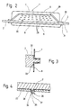
- the housing 1 has a closed plastic frame 2 produced by injection molding. On the top 3 and the bottom 4 of the plastic frame 2, two plastic housing shells 5 and 6 are attached.
- the housing plastic shell 5 forms a trough-shaped, relatively deep upper shell 7 and the housing plastic shell 6 is designed as a trough-shaped but flatter lower shell 8.
- FIG. 1 this has four frame legs 9, 10, 11 and 12 which are integrally connected to one another.
- a heat conducting web 13 of a heat sink 14 is embedded in the frame leg 10.
- the heat conducting web 13 is thus extrusion-coated with plastic during the manufacture of the plastic frame 2.
- the heat conducting web 13 merges at one end 15 into an angled component mounting surface 16.
- the other end 17 of the heat conducting web 13 is connected in one piece to a heat dissipation element 18 located outside the plastic frame 12.
- the heat dissipation elements 18 each have a bore 19 for fastening elements, so that they form fastening connections 20 for the plastic frame 2 and thus for the housing 1.
- molded-on tabs 21 can also be formed on the plastic frame 2, which are provided with mounting holes 22 (see frame leg 12 in FIG. 1). Since the mounting connections 20 and the tabs 21 jump out over the frame periphery, flanges 23 'are formed from these elements, the one enable particularly simple assembly of the housing 1.
- a circuit board 23 is fastened to the frame legs 9, 10, 11 and 12 and has an electronic circuit, preferably control unit electronics (not shown).
- the circuit board 23 is either located inside the frame or it is arranged on the underside 4 of the plastic frame 2 such that no frame parts protrude beyond the underside of the circuit board 23.
- metal pins 24 molded into the plastic frame 2 are provided, which engage in bores 25 of the printed circuit board 23 and hold the latter by bending on the underside of the printed circuit board.
- the bores 25 are assigned metallic / metallized areas, in particular conductor tracks, so that the circuit board is held by the bent metal pins 24 until a soldering process and there is a firm connection between the metal pins 24 and the circuit board 23 after the soldering.
- the printed circuit board 23 may be held on the plastic frame 2 by means of screws.
- a connector plug 26 is provided, which is embedded in the frame leg 11 of the plastic frame 2. It is extrusion-coated with plastic during the manufacture of the plastic frame 2, so that a gap-free seal is ensured.
- the contact tabs 27 of the contacts 28 of the connector 26 are connected in a suitable manner to the electronic circuit arranged on the printed circuit board 23, the latter having heat-generating power components (not shown) which are arranged on the component mounting surface 16 of the heat sink 14 with the lowest possible heat transfer resistance.
- the connector plug 26 it is alternatively also possible for the connector plug 26 to be arranged on the upper side 3 of the plastic frame 2, the upper shell 7 of the housing 1 having a shape-matched edge contour 29 which bears tightly against the upper side of the connector plug 26.
- Upper shell 7 and lower shell 8 have angled edge webs 30 and 31, which are welded all round to the top 3 and the bottom 4 of the plastic frame 2. This is preferably carried out in one operation, namely in the so-called plister process, the two housing plastic shells 5 and 6 being sealed by sealing a suitable tool with a heated tool stamp to the plastic frame 2.
- the plastic housing shells 5 and 6 are provided with a metallization. For this they are either steamed with metal or with equipped with a metal insert. They can be produced using the injection molding process or the deep-drawing process.
- the lower shell 8 is first inserted into a tool, then the plastic frame 2 with the printed circuit board 23 attached to it is placed on the lower shell 8 in a position aligned by suitable joining aids, and finally the housing is completed by applying the upper shell 7.
- printed circuit board blanks are preferably used, on which several plastic frames 2 can be placed, so that several printed circuit boards can simultaneously be moved over a soldering bath by means of the metal pins 24 described above. After soldering, the individual printed circuit boards 23 with the plastic frames 2 attached to them are broken out or punched out of the printed circuit board. This makes the production particularly economical.
- FIG. 3 shows that the plastic frame 2 can be designed step-like in the fastening area with the housing plastic shells 5 and 6.
- the upper shell 7 engages in one stage 32 and the lower shell 8 engages in the other stage 33.
- the connection area between the shells and the frame is thus formed over a particularly large area, so that an absolutely tight connection is produced during welding. Instead of welding, gluing can also take place.
- each snap projection 34 has a web 35 which has a head-shaped end region 36. Head area 36 and web 35 are provided with a slot 37.
- the printed circuit board 23 has bores 38 which are adapted to the diameter of the web 35.
- the holes 38 are pressed onto the snap projections 34, the head-shaped end region 36 being reduced in diameter due to the slot 37, so that the web 35 can engage in the bore 38.
- the end region 36 springs apart again, so that a grip behind the printed circuit board 23 is created.
Landscapes
- Physics & Mathematics (AREA)
- Thermal Sciences (AREA)
- Engineering & Computer Science (AREA)
- Microelectronics & Electronic Packaging (AREA)
- Cooling Or The Like Of Electrical Apparatus (AREA)
- Casings For Electric Apparatus (AREA)
Abstract
Claims (9)
- Boîtier (1) destiné à recevoir un circuit électronique (25) équipé d'un connecteur à broches, notamment une électronique de commande d'un moteur à combustion interne de véhicule, comportant un cadre (2), sur lequel est fixé un circuit imprimé (23) portant le circuit électronique, un refroidisseur (14) associé aux éléments de puissance du circuit, ainsi qu'une enveloppe (5, 6) recouvrant le circuit imprimé, caractérisé en ce que le cadre est un cadre en plastique (2) réalisé par injection, incorporant au moulage au moins une lame thermoconductrice (13) du refroidisseur (14), l'une des extrémités de la lame jouant le rôle, à l'intérieur du cadre, de portée de montage (16) de composants tandis que l'autre extrémité (17) constitue, à l'extérieur du cadre, l'élément (18) d'évacuation de la chaleur.
- Boîtier selon la revendication 1, caractérisé en ce que l'élément (18) d'évacuation de la chaleur constitue un raccord de fixation (20) du boîtier.
- Boîtier selon la revendication 2, caractérisé en ce que le raccord de fixation (20) du boîtier est constitué par une bride (23′) percée d'un trou (19) destiné à un élément de fixation.
- Boîtier selon une des revendications précédentes, caractérisé en ce que le connecteur à broches (26) est incorporé, au moulage, dans le cadre en plastique (2).
- Boîtier selon une des revendications précédentes, caractérisé en ce que le cadre en plastique (2) comporte des tétons d'encliquetage (34) moulés, qui peuvent être bloqués dans des trous (38) du circuit imprimé (23).
- Boîtier selon une des revendications précédentes, caractérisé en ce que des broches métalliques (24), incorporées lors du moulage dans le cadre en plastique (2), sont engagées dans des trous (25) du circuit imprimé et, par rabattement, maintiennent celui-ci.
- Boîtier selon la revendication 6, caractérisé en ce que les broches métalliques (24) maintiennent, par leur rabattement, le circuit imprimé jusqu'au moment de la soudure du circuit imprimé, tandis que des zones métalliques ou métallisées, en particulier des pistes conductrices, sont associées aux trous (25) du circuit (23) de maniére qu'après l'opération de soudure, il existe une liaison durable par soudure entre les broches métalliques (24) et le circuit imprimé (23).
- Boîtier selon une des revendications précédentes, caractérisé en ce que l'enveloppe est constituée de deux coques (5 6) de boîtier, en matière plastique, reliées aux faces supérieure et inférieure (3, 4) du cadre, notamment par soudure.
- Boîtier selon la revendication 8, caractérisé en ce que les coques (5, 6) sont métallisées.
Applications Claiming Priority (3)
| Application Number | Priority Date | Filing Date | Title |
|---|---|---|---|
| DE3933123 | 1989-10-04 | ||
| DE3933123A DE3933123A1 (de) | 1989-10-04 | 1989-10-04 | Gehaeuse fuer eine elektronische schaltung |
| PCT/DE1990/000741 WO1991005451A1 (fr) | 1989-10-04 | 1990-09-28 | Boitier pour circuits electroniques |
Publications (2)
| Publication Number | Publication Date |
|---|---|
| EP0446323A1 EP0446323A1 (fr) | 1991-09-18 |
| EP0446323B1 true EP0446323B1 (fr) | 1994-07-13 |
Family
ID=6390813
Family Applications (1)
| Application Number | Title | Priority Date | Filing Date |
|---|---|---|---|
| EP90914067A Expired - Lifetime EP0446323B1 (fr) | 1989-10-04 | 1990-09-28 | Boitier pour circuits electroniques |
Country Status (5)
| Country | Link |
|---|---|
| US (1) | US5118903A (fr) |
| EP (1) | EP0446323B1 (fr) |
| JP (1) | JP2930135B2 (fr) |
| DE (2) | DE3933123A1 (fr) |
| WO (1) | WO1991005451A1 (fr) |
Cited By (1)
| Publication number | Priority date | Publication date | Assignee | Title |
|---|---|---|---|---|
| DE102004029536A1 (de) * | 2004-06-18 | 2006-01-05 | Robert Bosch Gmbh | EMV-Stitchpin |
Families Citing this family (23)
| Publication number | Priority date | Publication date | Assignee | Title |
|---|---|---|---|---|
| DE4215041C3 (de) * | 1991-05-22 | 1997-09-25 | Siemens Ag | Elektronisches Steuergerät |
| US5237486A (en) * | 1992-06-05 | 1993-08-17 | Apple Computer, Inc. | Structural frame for portable computer |
| GB9308060D0 (en) * | 1993-04-19 | 1993-06-02 | Cancer Res Campaign Tech | Stem cell inhibitor |
| US5455741A (en) * | 1993-10-26 | 1995-10-03 | Pulse Engineering, Inc. | Wire-lead through hole interconnect device |
| JP3051011B2 (ja) * | 1993-11-18 | 2000-06-12 | 株式会社東芝 | パワ−モジュ−ル |
| DE4445125A1 (de) | 1994-12-17 | 1996-06-20 | Wabco Gmbh | Gehäuse für ein elektrisches Bauteil |
| US5586005A (en) * | 1995-03-16 | 1996-12-17 | International Business Machines Corporation | Removable heat sink assembly for a chip package |
| US6005463A (en) * | 1997-01-30 | 1999-12-21 | Pulse Engineering | Through-hole interconnect device with isolated wire-leads and component barriers |
| DE19703676C2 (de) | 1997-01-31 | 2002-01-24 | Siemens Ag | Verfahren und Vorrichtung zum toleranzgenauen Verbinden zweier Bauteile |
| JP3248480B2 (ja) * | 1998-01-22 | 2002-01-21 | 住友電装株式会社 | 配電ボックス |
| US6055158A (en) * | 1999-03-16 | 2000-04-25 | Framatome Connectors Interlock, Inc. | Electronic component heat sink assembly |
| TW420969B (en) * | 2000-01-28 | 2001-02-01 | Metal Ind Redearch & Dev Ct | Method of producing thin metal case with joint element |
| DE10020018A1 (de) | 2000-04-22 | 2001-11-08 | Brose Fahrzeugteile | Elektromechanische Antriebsvorrichtung |
| US6377462B1 (en) | 2001-01-09 | 2002-04-23 | Deere & Company | Circuit board assembly with heat sinking |
| DE10247828B4 (de) * | 2002-10-14 | 2005-03-03 | Siemens Ag | Wärmeableitendes und -abstrahlendes Kuststoffgehäuse mit Kühl-/Tragrippen und umpritztem Kühlkörper und Verfahren zu dessen Fertigung |
| DE102006006846B3 (de) * | 2006-02-15 | 2007-08-30 | Tyco Electronics Amp Gmbh | Elektrischer Leistungsverteiler und elektrisches Stanzgitter dafür |
| EP2040524A1 (fr) * | 2007-09-24 | 2009-03-25 | Siemens Aktiengesellschaft | Procédé destiné à la fabrication d'un appareil électronique, en particulier d'un module de puissance, appareil électrique et contact de raccordement |
| JP5184286B2 (ja) * | 2008-09-30 | 2013-04-17 | 富士通テン株式会社 | 筐体固定構造 |
| JP6310791B2 (ja) * | 2014-06-25 | 2018-04-11 | 矢崎総業株式会社 | スイッチボックス |
| CN105140170B (zh) * | 2015-08-31 | 2017-12-22 | 北京航天控制仪器研究所 | 一种可实现精对准的多陶瓷管壳封帽夹具 |
| DE102019203017A1 (de) | 2019-03-06 | 2020-09-10 | Robert Bosch Gmbh | Bauteilanordnung mit einer Verbindung zwischen zwei Bauteilen |
| EP4149224A1 (fr) | 2021-09-09 | 2023-03-15 | Stryker European Operations Limited | Ensemble boîtier pour accueillir des cartes de circuits imprimés |
| DE102023127630A1 (de) * | 2023-10-10 | 2025-04-10 | Lisa Dräxlmaier GmbH | Gehäuse für ein elektronisches bauteil, anordnung mit einem gehäuse und verfahren zur herstellung eines gehäuses |
Family Cites Families (12)
| Publication number | Priority date | Publication date | Assignee | Title |
|---|---|---|---|---|
| US3869563A (en) * | 1973-09-27 | 1975-03-04 | Motorola Inc | Encapsulation housing for electronic circuit boards or the like and method of encapsulating |
| US3904262A (en) * | 1974-09-27 | 1975-09-09 | John M Cutchaw | Connector for leadless integrated circuit packages |
| DE2546334C2 (de) * | 1975-10-16 | 1984-10-11 | Robert Bosch Gmbh, 7000 Stuttgart | Elektronisches Steuergerät |
| DE3020902A1 (de) * | 1980-06-02 | 1981-12-17 | Robert Bosch Gmbh, 7000 Stuttgart | Elektronisches steuergeraet, insbesondere fuer kraftfahrzeuge |
| US4679118A (en) * | 1984-08-07 | 1987-07-07 | Aavid Engineering, Inc. | Electronic chip-carrier heat sinks |
| GB2197755B (en) * | 1986-08-20 | 1990-05-09 | Plessey Co Plc | Electronic circuit housing |
| US5019940A (en) * | 1987-02-24 | 1991-05-28 | Thermalloy Incorporated | Mounting apparatus for electronic device packages |
| US4811165A (en) * | 1987-12-07 | 1989-03-07 | Motorola, Inc. | Assembly for circuit modules |
| FR2629665B1 (fr) * | 1988-03-30 | 1991-01-11 | Bendix Electronics Sa | Boitier pour circuit electronique |
| FR2634617A1 (fr) * | 1988-07-22 | 1990-01-26 | Neiman Sa | Module electronique emboite |
| DE3837974A1 (de) * | 1988-11-09 | 1990-05-10 | Telefunken Electronic Gmbh | Elektronisches steuergeraet |
| JP2612339B2 (ja) * | 1989-04-18 | 1997-05-21 | 三菱電機株式会社 | 電子機器筐体 |
-
1989
- 1989-10-04 DE DE3933123A patent/DE3933123A1/de not_active Withdrawn
-
1990
- 1990-09-28 EP EP90914067A patent/EP0446323B1/fr not_active Expired - Lifetime
- 1990-09-28 DE DE59006436T patent/DE59006436D1/de not_active Expired - Fee Related
- 1990-09-28 WO PCT/DE1990/000741 patent/WO1991005451A1/fr not_active Ceased
- 1990-09-28 JP JP2513114A patent/JP2930135B2/ja not_active Expired - Lifetime
- 1990-09-28 US US07/679,031 patent/US5118903A/en not_active Expired - Fee Related
Cited By (1)
| Publication number | Priority date | Publication date | Assignee | Title |
|---|---|---|---|---|
| DE102004029536A1 (de) * | 2004-06-18 | 2006-01-05 | Robert Bosch Gmbh | EMV-Stitchpin |
Also Published As
| Publication number | Publication date |
|---|---|
| DE3933123A1 (de) | 1991-04-11 |
| JPH04502090A (ja) | 1992-04-09 |
| EP0446323A1 (fr) | 1991-09-18 |
| DE59006436D1 (de) | 1994-08-18 |
| JP2930135B2 (ja) | 1999-08-03 |
| WO1991005451A1 (fr) | 1991-04-18 |
| US5118903A (en) | 1992-06-02 |
Similar Documents
| Publication | Publication Date | Title |
|---|---|---|
| EP0446323B1 (fr) | Boitier pour circuits electroniques | |
| EP1208618B1 (fr) | Appareil de commande et procede de soudage | |
| EP0588793B1 (fr) | Boitier pour composants electroniques d'automobile | |
| DE10134639B4 (de) | Gehäuse für ein elektronisches Steuergerät in Fahrzeugen | |
| EP0712265B1 (fr) | Assemblage électronique | |
| DE10392749B4 (de) | Kontrollmodulgehäuse für ein Fahrzeug | |
| AT503687B1 (de) | Steuergerät mit einem stirnseitig kontaktierten schaltungsträger | |
| DE3936906A1 (de) | Gehaeuse fuer kfz-elektronik | |
| EP0708583A1 (fr) | Appareil électrique et sa fabrication | |
| DE102006016775A1 (de) | Elektronische Vorrichtung und Verfahren zum Herstellen der Gleichen | |
| DE102008051545B4 (de) | Elektronisches Gerät mit Mehrkontaktstecker und Verfahren zur Herstellung desselben | |
| WO2005025940A1 (fr) | Unite appareil de commande et son procede de production | |
| EP0717588A2 (fr) | Boîtier pour un dispositif électrique | |
| WO1992000660A1 (fr) | Boitier pour un circuit electronique | |
| DE4232048A1 (de) | Elektronisches Steuergerät | |
| DE10304889A1 (de) | Elektronikleiterplattengehäuse und Verfahren zur Herstellung einer Elektronikschaltungseinheit | |
| EP0526466B1 (fr) | Dispositif electrique de commutation et de commande, en particulier pour vehicules automobiles | |
| EP1282345B1 (fr) | Boîtier abritant une carte électronique avec ses composants dans un véhicule | |
| DE3933124A1 (de) | Elektronisches geraet mit flexiblem leiterplattenbereich | |
| EP2514285B1 (fr) | Élément de fermeture pour un boîtier | |
| DE102012105352A1 (de) | Positionierelement | |
| DE102017210176A1 (de) | Elektronikmodul | |
| DE19837552C1 (de) | Füllstandsgeber für eine Betriebsflüssigkeit in einem Kraftfahrzeug, insbesondere Ölfüllstandsgeber | |
| EP0728405B1 (fr) | Dispositif permettant d'evacuer la chaleur de dissipation d'un composant electronique ou electromecanique | |
| EP0452641B1 (fr) | Eléments de fixation enfichables pour circuits imprimés |
Legal Events
| Date | Code | Title | Description |
|---|---|---|---|
| PUAI | Public reference made under article 153(3) epc to a published international application that has entered the european phase |
Free format text: ORIGINAL CODE: 0009012 |
|
| 17P | Request for examination filed |
Effective date: 19910507 |
|
| AK | Designated contracting states |
Kind code of ref document: A1 Designated state(s): DE FR GB IT |
|
| RAP3 | Party data changed (applicant data changed or rights of an application transferred) |
Owner name: ROBERT BOSCH GMBH |
|
| 17Q | First examination report despatched |
Effective date: 19931130 |
|
| GRAA | (expected) grant |
Free format text: ORIGINAL CODE: 0009210 |
|
| AK | Designated contracting states |
Kind code of ref document: B1 Designated state(s): DE FR GB IT |
|
| ET | Fr: translation filed | ||
| REF | Corresponds to: |
Ref document number: 59006436 Country of ref document: DE Date of ref document: 19940818 |
|
| ITF | It: translation for a ep patent filed | ||
| GBT | Gb: translation of ep patent filed (gb section 77(6)(a)/1977) |
Effective date: 19940919 |
|
| PLBE | No opposition filed within time limit |
Free format text: ORIGINAL CODE: 0009261 |
|
| STAA | Information on the status of an ep patent application or granted ep patent |
Free format text: STATUS: NO OPPOSITION FILED WITHIN TIME LIMIT |
|
| 26N | No opposition filed | ||
| PGFP | Annual fee paid to national office [announced via postgrant information from national office to epo] |
Ref country code: GB Payment date: 20000911 Year of fee payment: 11 |
|
| PGFP | Annual fee paid to national office [announced via postgrant information from national office to epo] |
Ref country code: FR Payment date: 20000921 Year of fee payment: 11 |
|
| PGFP | Annual fee paid to national office [announced via postgrant information from national office to epo] |
Ref country code: DE Payment date: 20001129 Year of fee payment: 11 |
|
| PG25 | Lapsed in a contracting state [announced via postgrant information from national office to epo] |
Ref country code: GB Free format text: LAPSE BECAUSE OF NON-PAYMENT OF DUE FEES Effective date: 20010928 |
|
| REG | Reference to a national code |
Ref country code: GB Ref legal event code: IF02 |
|
| PG25 | Lapsed in a contracting state [announced via postgrant information from national office to epo] |
Ref country code: DE Free format text: LAPSE BECAUSE OF NON-PAYMENT OF DUE FEES Effective date: 20020501 |
|
| GBPC | Gb: european patent ceased through non-payment of renewal fee |
Effective date: 20010928 |
|
| PG25 | Lapsed in a contracting state [announced via postgrant information from national office to epo] |
Ref country code: FR Free format text: LAPSE BECAUSE OF NON-PAYMENT OF DUE FEES Effective date: 20020531 |
|
| REG | Reference to a national code |
Ref country code: FR Ref legal event code: ST |
|
| PG25 | Lapsed in a contracting state [announced via postgrant information from national office to epo] |
Ref country code: IT Free format text: LAPSE BECAUSE OF NON-PAYMENT OF DUE FEES Effective date: 20050928 |