EP0446441B1 - Système de multiplexage flexible - Google Patents
Système de multiplexage flexible Download PDFInfo
- Publication number
- EP0446441B1 EP0446441B1 EP90123452A EP90123452A EP0446441B1 EP 0446441 B1 EP0446441 B1 EP 0446441B1 EP 90123452 A EP90123452 A EP 90123452A EP 90123452 A EP90123452 A EP 90123452A EP 0446441 B1 EP0446441 B1 EP 0446441B1
- Authority
- EP
- European Patent Office
- Prior art keywords
- parallel
- serial
- data
- multiplex
- clock
- Prior art date
- Legal status (The legal status is an assumption and is not a legal conclusion. Google has not performed a legal analysis and makes no representation as to the accuracy of the status listed.)
- Expired - Lifetime
Links
- 101150085905 DCP2 gene Proteins 0.000 claims description 7
- 101100031494 Schizosaccharomyces pombe (strain 972 / ATCC 24843) psu1 gene Proteins 0.000 claims description 7
- 101100422754 Schizosaccharomyces pombe (strain 972 / ATCC 24843) sui1 gene Proteins 0.000 claims description 7
- 101100331197 Arabidopsis thaliana DEK2 gene Proteins 0.000 claims description 2
- 101150011387 DEK1 gene Proteins 0.000 claims description 2
- 101100331195 Oryza sativa subsp. japonica ADL1 gene Proteins 0.000 claims description 2
- 101150055492 sel-11 gene Proteins 0.000 claims description 2
- 230000011664 signaling Effects 0.000 abstract description 6
- 230000037431 insertion Effects 0.000 abstract 1
- 238000003780 insertion Methods 0.000 abstract 1
- 230000005540 biological transmission Effects 0.000 description 11
- 101000821827 Homo sapiens Sodium/nucleoside cotransporter 2 Proteins 0.000 description 2
- 102100021541 Sodium/nucleoside cotransporter 2 Human genes 0.000 description 2
- 238000006243 chemical reaction Methods 0.000 description 2
- 101000685663 Homo sapiens Sodium/nucleoside cotransporter 1 Proteins 0.000 description 1
- 102100023116 Sodium/nucleoside cotransporter 1 Human genes 0.000 description 1
- 241000544066 Stevia Species 0.000 description 1
- 230000015556 catabolic process Effects 0.000 description 1
- 238000011161 development Methods 0.000 description 1
- 230000018109 developmental process Effects 0.000 description 1
- 238000012432 intermediate storage Methods 0.000 description 1
- 238000000034 method Methods 0.000 description 1
- HELXLJCILKEWJH-NCGAPWICSA-N rebaudioside A Chemical compound O([C@H]1[C@H](O)[C@@H](CO)O[C@H]([C@@H]1O[C@H]1[C@@H]([C@@H](O)[C@H](O)[C@@H](CO)O1)O)O[C@]12C(=C)C[C@@]3(C1)CC[C@@H]1[C@@](C)(CCC[C@]1([C@@H]3CC2)C)C(=O)O[C@H]1[C@@H]([C@@H](O)[C@H](O)[C@@H](CO)O1)O)[C@@H]1O[C@H](CO)[C@@H](O)[C@H](O)[C@H]1O HELXLJCILKEWJH-NCGAPWICSA-N 0.000 description 1
- 230000008672 reprogramming Effects 0.000 description 1
Images

Classifications
-
- H—ELECTRICITY
- H04—ELECTRIC COMMUNICATION TECHNIQUE
- H04J—MULTIPLEX COMMUNICATION
- H04J3/00—Time-division multiplex systems
- H04J3/16—Time-division multiplex systems in which the time allocation to individual channels within a transmission cycle is variable, e.g. to accommodate varying complexity of signals, to vary number of channels transmitted
- H04J3/1605—Fixed allocated frame structures
- H04J3/1623—Plesiochronous digital hierarchy [PDH]
- H04J3/1647—Subrate or multislot multiplexing
Definitions
- the invention relates to a flexible multiplex system with a multiplex device and a demultiplex device according to the preambles of claims 1 and 2.
- the multiplex and the demultiplex device are designed in particular for a configurable fixed network with a transmission bit rate of 64 kbit / s. Regardless of this, the principle of the multiplexing and demultiplexing device can be used in any system.
- a circuit arrangement for generating a time-division multiplex signal is known from European patent application EP 0 176 148 A2, in which the signals of the input lines are converted into parallel signals by serial-parallel converters, which are fed to a parallel-serial converter to form the multiplex signal. Processing of input signals with different clock rates is not provided.
- the object of the invention is to provide a flexible multiplex device and a corresponding demultiplex device with little effort for a multiplex system.
- the simple and flexible subscriber channel structure that can be controlled by a memory is advantageous. Functional reliability is improved by the decoder, since only one data output can always be switched from the data bus, and the amount of memory is still increased be reduced.
- the division of the multiplex channel into certain subscriber channels automatically results in the bit rate for each subscriber channel and an assigned bit clock, which is switched through by a central clock supply via clock multiplexers. The prerequisite is that a suitable fixed pulse frame is always specified.
- serial-parallel conversion of the input data is advantageous. This results in an automatic intermediate storage, which enables a clear structure with the help of a data bus.
- the flexible demultiplexer is designed accordingly. Only the synchronization is added.
- the demultiplexing device can be constructed independently of the multiplexing device. This also enables the channels to be routed between any inputs of the multiplex device and outputs of the demultiplex device.
- a suitable pulse frame PR which was specified by Nyhoff, is shown in part in FIG.
- the pulse frame contains 80 code words with 8 bits each. Each of these bytes is labeled.
- the first byte SO1 and another byte SO2 are used for synchronization.
- Other bytes denoted by Dxx are combined to form a signaling channel SK.
- all bytes designated with Axx, Bxx or Cxx are used for the actual data transmission.
- the complete pulse frame - divided into eight lines - is shown in Table 1. If all bytes suitable for data transmission are used for transmission, this results in a transmission rate of 57,600 bit / s.
- This transmission capacity can be divided into three channels K31 to K33 with a transmission rate of 19,200 bit / s each. This division is shown in Table 2.
- up to 6 channels K61 to K66 with 9,600 bit / s each 12 channels K12.1 to K12.12 with 4,800 bit / s each or 24 channels K24 .1 to K24.24 can be formed with 2,400 bit / s each.
- a customary subscriber channel structure is composed of the above-mentioned channels with different data rates.
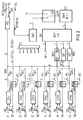
- FIG. 2 shows a flexible multiplex device for 6 subscriber channels CH1 to CH6 and thus also for 6 data terminal devices.
- a serial-to-parallel converter SPU1 to SPU6 is assigned to each subscriber channel, to which the input data are serially supplied via an input E1 to E6.
- the corresponding bit clock BT1 to BT6 is present at the clock input of the serial-parallel converter and is output to the respective data terminal device via clock outputs TA1 to TA6.
- the outputs of the serial-to-parallel converter are connected to a data bus DBM with a word length of 8 bits, which is connected to a parallel-to-serial converter PSU.
- the clock inputs of the serial-parallel converter are connected to a clock supply TVS (not shown) via clock multiplexers CMUX1 to CMUX6. They are controlled by an IFS transmission interface.
- a transmission-side memory controller STS is addressed via a changeover switch US1, the data output of which is controlled via a decoder DEK Selects inputs SE1 to SE6 of the serial-to-parallel converter and the three word generators WG1 to WG3, whose outputs can also be switched to the data bus DBM.
- the distribution of the available transmission capacity among the individual subscriber channels is carried out by programming the memory controller STS, which is designed, for example, as RAM.
- the decoder DEK1 converts the binary input data into one of nine possible output signals to its decoder output DA1, i.e. only one of its nine outputs is active at a time and therefore only switches one of the serial-to-parallel converters or a word generator on the data bus.
- the coding can of course also be taken over directly by the memory controller, but then the word width would then also have to be expanded from four to nine bits.
- the clock supply not only supplies the multiplex signal clock TMS, but also the bit clocks BT derived therefrom and the word clock WT1 for the address counter CNT.
- the counting capacity of the address counter coincides with the number of data words of the pulse frame according to Table 1, so here it includes the counter positions 0 to 79 (mod 80).
- the first frame identifier word SO1 is first output to the parallel-serial converter by the second word generator WG2, converted into serial data and output at the multiplexer output MA.
- the address counter then increases the address SA1 of the memory controller STS by 1, whereupon the first data word in the time slot AO1 is taken over from the first serial-to-parallel converter SPU1.
- the transfer takes place with the corresponding select signal sel1, so that an original byte structure at the output of the first serial-to-parallel converter 1 is generally lost.
- the same assignment takes place again in the demultiplexing device, so that transparent data transmission is ensured.
- a data byte of the second serial-to-parallel converter SPU2 is taken over and transmitted by the parallel-to-serial converter PSU via the data bus DBM, etc
- Table 6 shows a breakdown of five subscriber channels with different speeds.
- Table 7 shows the associated addressing of the memory locations in hexadecimal notation.
- the serial-to-parallel converters each contain a shift register and a memory register, in each of which one byte is stored. Since the time slots of the pulse frame are divided evenly between the different subscriber channels, the transfer to the parallel-serial converter is easy.
- Each serial-parallel converter contains the correct bit clock via a clock multiplexer CMUX1 to CMUX6 which was selected by an interface IFS from four different clock signals with a frequency between 2.4 and 19.2 kHz.
- the interface is programmed according to the STS memory controller. Any register or an output port of a microcomputer can be used as an interface.
- the address input of the memory controller and its data input (not shown in FIG. 2) are connected to a programming device PE and, like the interface, is loaded with the corresponding data.
- the subscriber channel structure and the assignment of the channels to time slots in the pulse frame PR can be determined by a central network controller.
- microcomputer can be interposed as a programming unit PE, which loads the corresponding data into the memory controller STS, STE.
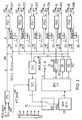
- a demultiplexing device is shown in FIG.
- the received multiplex signal MS is fed to a serial-to-parallel converter SPU via a multiplexer input ME and simultaneously to the data inputs from the parallel-to-serial converters PSU1 to PSU6 via a data bus DBD.
- the serial outputs of the parallel-serial converter form the data outputs A1 to A6.
- Bit clock signals of different frequencies are fed from a receiving clock supply TVE via clock multiplexers CMUX11 to CMUX16 to a clock input of a parallel-serial converter and at the same time via assigned clock outputs TA11 to TA16 delivered.
- the multiplexers are controlled accordingly via a receiving interface IFE.
- the memory controller STE at the receiving end and the associated decoder DEK2 are constructed in accordance with the multiplexing device.
- a second address counter CNT2 is in turn connected to the memory controller STE via a second changeover switch US2.
- the memory controller STE can be switched on to the programming device PE via this switch.
- the demultiplexing device requires synchronization SYNC.
- the multiplex signal is fed to two comparison devices VE1 and VE2 which, when a frame code word SO1 or SO2 is present, emit a corresponding signal to the synchronization, which then enables the address counter CNT2. In order to avoid incorrect synchronization, all known frame synchronization methods can be used.
- SR which is also connected to the data bus DBD and into which the data is transferred under the control of the decoder.
- the multiplex signal MS received at the demultiplexer input DE is fed to the serial-parallel converter SPU with a receive clock TME and converted into parallel data words.
- This parallelized multiplex signal is supplied via the data bus DBD to all parallel-serial converters PSU1 to PSU6.
- the corresponding data words are then controlled by the receive-side memory controller STE - controlled by the selective signals sel11 to sel16 led to the selective inputs SE11 to SE16 by the parallel-serial converters PSU1 to PSU6 taken over and converted again into a continuous serial data stream for each subscriber channel CH1 to CH6.
- the receive-side memory controller STE will be programmed accordingly to the transmit-side memory controller STS.
- a subscriber channel CH1 assigned to the data input D1 in the demultiplexing device may assign another data output, for example data output A4.
- the words of the signaling channel are transferred directly to the signaling register SR and can be called up in parallel at the signaling output SA. If necessary, the conversion can also take place here via a further parallel-serial converter into a serial data stream.
- the same clock supply is used for the multiplexing and demultiplexing device, which then generates all word and bit clock signals.
Landscapes
- Engineering & Computer Science (AREA)
- Computer Networks & Wireless Communication (AREA)
- Signal Processing (AREA)
- Time-Division Multiplex Systems (AREA)
- Input Circuits Of Receivers And Coupling Of Receivers And Audio Equipment (AREA)
- Laying Of Electric Cables Or Lines Outside (AREA)
- Joints Allowing Movement (AREA)
- Vehicle Body Suspensions (AREA)
- Eye Examination Apparatus (AREA)
- Electrotherapy Devices (AREA)
- Preparation Of Compounds By Using Micro-Organisms (AREA)
Claims (7)
- Système de multiplexage souple comportant un dispositif de multiplexage, qui comporte plusieurs entrées de données (E1,E2,...) pour le raccordement de terminaux de transmission de données, et un multiplexeur pour la formation d'un signal de multiplexage (MS), et dans lequel à chaque entrée de données (E1 à E6) est associé un convertisseur série/parallèle (SPU1 à SPU6), dont les sorties en parallèle sont raccordées à un bus de transmission de données (DBM), auquel sont également raccordées les entrées d'un convertisseur parallèle/série (PSU), qui délivre le signal de multiplexage (MS) à sa sortie,
caractérisé par le fait
qu'il est prévu une unité de commande de mémoire (STS) située côté émission et dont l'adresse (SA1) est modifiée pas-à-pas par l'intermédiaire d'un compteur d'adresses (CNT1), que les données de sortie de l'unité de commande de mémoire sont converties en des signaux de sélection (Sel1, Sel6), qui commandent le transfert des données des convertisseurs série/parallèle (SPU1 à SPU6) par l'intermédiaire de leurs entrées de sélection (SE1 à SE6), en fonction d'une structure prévue de canaux d'abonnés, et que le signal de cadence binaire (BT1 à BT6), qui correspond au canal d'abonné respectif (CH1 à CH6), est envoyé à chaque convertisseur série/parallèle (SPU1, SPU6) à partir d'une unité d'alimentation de cadence (TVS), qui délivre les signaux de cadence binaire possédant plusieurs fréquences différentes, par l'intermédiaire d'un multiplexeur de cadence (CMUX1 à CMUX6). - Système de multiplexage souple comportant un dispositif de démultiplexage, qui possède plusieurs sorties de données (A1 à A6) pour le raccordement de terminaux de traitement de données de la transmission de données et qui possède un démultiplexeur servant à répartir un signal de multiplexage (MS) entre différents canaux d'abonnés (CH1 à CH6) et dans lequel est prévu un dispositif de synchronisation (SYNC), et dans lequel le signal de multiplexage reçu (MS) est envoyé à un convertisseur série/parallèle (SPU) et les sorties en parallèle du convertisseur série/parallèle (SPU) sont raccordées par l'intermdiaire d'un bus de transmission de données (DBD) aux entrées en parallèle de convertisseurs parallèle-série (PSU1 à PSU6), dont la réception des données peut être activée par l'intermédiaire d'entrées de sélection (SE11 à SE16),
caractérisé par le fait
qu'il est prévu une unité de commande de mémoire (STE) prévue sur le côté réception et dont l'adresse de mémoire (SA2) est modifiée pas-à-pas par l'intermédiaire d'un second compteur d'adresses (CNT2) et dont les données de sortie sont converties en des signaux de sélection (sel 11 à sel 16), qui commandent les convertisseurs parallèle/série (PSU1 à PSU6) en fonction d'une structure choisie de canal d'abonné, que le signal de cadence binaire (BT11 à BT16), qui correspond au canal d'abonné respectif (CH1 à CH6) est envoyé à chaque convertisseur parallèle/série (PSU1 à PSU6), par une unité d'alimentation de cadence (TVE), qui délivre des signaux de cadence binaire possédant plusieurs cadences différentes, par l'intermédiaire d'un multiplexeur de cadence (CMUX11 à CMUX16). - Système de multiplexage souple suivant la revendication 1 ou 2, caractérisé par le fait qu'aux sorties de l'unité de commande de mémoire (STS,STE) est raccordé un codeur (DEK1, DEK2), qui délivre un signal logique actif, respectivement uniquement sur l'une de ses sorties (DA1,DA2).
- Système de multiplexage souple suivant l'une des revendications précédentes, caractérisé par le fait que le compteur (CNT1,CNT2) possède respectivement une plage de contact qui correspond à l'ensemble des mots de la trame d'impulsions (PR).
- Système de multiplexage souple suivant l'une des revendications précédentes, caractérisé par le fait que l'unité de commande de mémoire (STS,STE) est programmable ou interchangeable et qu'il est prévu une interface (IFS,IFE) programmagle, réglable ou interchangeable de façon correspondante et servant à commander les multiplexeurs de cadence (CMUX1 à CMUX6, CMUX11 à CMUX16.
- Système de multiplexage souple suivant l'une des revendications précédentes, caractérisé par le fait que les convertisseurs série/parallèle (SPU1 à SPU6) et les convertisseurs parallèle/série (PSU1 à PSU6) possèdent respectivement un registre de mémoire pour les mots de données présents en parallèle.
- Multiplexeur souple suivant l'une des revendications précédentes, caractérisé par le fait que le signal de multiplexage (MS) possède un débit de données de 64 kbits/s, et
que la trame d'impulsions contient 80 octets et que 4 à 10 canaux d'abonnés (CH1, CH2, ...) sont prévus.
Applications Claiming Priority (2)
| Application Number | Priority Date | Filing Date | Title |
|---|---|---|---|
| DE4007818 | 1990-03-12 | ||
| DE4007818 | 1990-03-12 |
Publications (3)
| Publication Number | Publication Date |
|---|---|
| EP0446441A2 EP0446441A2 (fr) | 1991-09-18 |
| EP0446441A3 EP0446441A3 (en) | 1991-11-21 |
| EP0446441B1 true EP0446441B1 (fr) | 1995-04-26 |
Family
ID=6402010
Family Applications (1)
| Application Number | Title | Priority Date | Filing Date |
|---|---|---|---|
| EP90123452A Expired - Lifetime EP0446441B1 (fr) | 1990-03-12 | 1990-12-06 | Système de multiplexage flexible |
Country Status (4)
| Country | Link |
|---|---|
| EP (1) | EP0446441B1 (fr) |
| AT (1) | ATE121888T1 (fr) |
| DE (1) | DE59008974D1 (fr) |
| NO (1) | NO910960L (fr) |
Families Citing this family (1)
| Publication number | Priority date | Publication date | Assignee | Title |
|---|---|---|---|---|
| DE19730623A1 (de) * | 1997-07-17 | 1999-01-21 | Alsthom Cge Alcatel | Verfahren zum Zuteilen von Zeitschlitzen, sowie System, Zentrale und Teilnehmereinrichtung zur Durchführung dieses Verfahrens |
Family Cites Families (2)
| Publication number | Priority date | Publication date | Assignee | Title |
|---|---|---|---|---|
| GB2128450B (en) * | 1982-10-04 | 1986-01-29 | Hitachi Ltd | Time-division switching unit |
| DE3435652A1 (de) * | 1984-09-28 | 1986-04-10 | Philips Patentverwaltung Gmbh, 2000 Hamburg | Schaltungsanordnung zum erzeugen eines zeitmultiplexsignals |
-
1990
- 1990-12-06 AT AT90123452T patent/ATE121888T1/de active
- 1990-12-06 EP EP90123452A patent/EP0446441B1/fr not_active Expired - Lifetime
- 1990-12-06 DE DE59008974T patent/DE59008974D1/de not_active Expired - Fee Related
-
1991
- 1991-03-11 NO NO91910960A patent/NO910960L/no unknown
Also Published As
| Publication number | Publication date |
|---|---|
| EP0446441A2 (fr) | 1991-09-18 |
| ATE121888T1 (de) | 1995-05-15 |
| DE59008974D1 (de) | 1995-06-01 |
| EP0446441A3 (en) | 1991-11-21 |
| NO910960D0 (no) | 1991-03-11 |
| NO910960L (no) | 1991-09-13 |
Similar Documents
| Publication | Publication Date | Title |
|---|---|---|
| DE3750394T2 (de) | Übertragungssteuerungssystem für Unterraten-Multimediadaten. | |
| EP0186141B1 (fr) | Multiplexeur démultiplexeur avec répartiteur de canaux pour signaux numériques de différents niveaux de hiérarchie | |
| DE2848255C2 (fr) | ||
| EP1280373B1 (fr) | Elément de réseau pour des signaux du réseau de transport optique | |
| DE2714368C3 (de) | Schaltungsanordnung zum Durchschalten von Datenwörtern unterschiedlicher Bitfolgefrequenz in Vielfachverbindungen | |
| EP0007524A1 (fr) | Procédé et circuit pour la transmission de données | |
| EP0598455B1 (fr) | Système de transmission pour la hiérarchie numérique synchrone | |
| DE3885489T2 (de) | Multiplexvorrichtung mit BSI-Codeverarbeitungs- und Bitverschachtelungsfunktionen. | |
| DE2520835C3 (de) | Schaltungsanordnung zur Übertragung von synchron und asynchron auftretenden Daten | |
| EP0446441B1 (fr) | Système de multiplexage flexible | |
| DE602004012066T2 (de) | Zeitmultiplexstreckenverbindungen zwischen einer Koppelmatrix und einem Port in einem Netzelement | |
| EP0103163B1 (fr) | Dispositif pour le démultiplexage synchrone d'un signal multiplex à division de temps | |
| EP0765050A2 (fr) | Méthode pour contrÔler la transmission de signaux numériques de communication par un support de transmission à multiplexage temporel | |
| EP0850517A1 (fr) | Element de reseau et unite d'entree/de sortie pour un systeme de transmission synchrone | |
| DE69738078T2 (de) | System und verfahren zur timing-kontrolle in einem distribuierten digitalen cross-connect-system | |
| DE3501674A1 (de) | Multiplexer/demultiplexer mit flexibler signalverarbeitungsfunktion fuer digitale zeitmultiplex-nachrichtenuebertragungssysteme | |
| EP0143268A2 (fr) | Procédé et dispositif pour intercaler un signal numérique binaire à bande étroite dans, ou pour extraire ce signal à bande étroite d'un signal à multiplexage dans le temps | |
| DE3107046C2 (fr) | ||
| EP0110360B1 (fr) | Montage de circuit pour rassembler et séparer des signaux de parole et des données lors de la transmission à travers un réseau de commutation numérique | |
| EP0176148A2 (fr) | Circuit pour la génération d'un signal multiplexé dans le temps | |
| AT390703B (de) | Wandlerschaltung zur zwischenschaltung zwischen digitalen und pulsamplitudenmodulierten signalen und zur wahlweisen modifizierung der digitalen signale | |
| DE69005866T2 (de) | Verfahren und Endeinrichtung zur Herstellung von Verbindungen über Kanäle, die in einer Multiplexverbindung ausgewählt sind. | |
| EP0482279B1 (fr) | Dispositif pour convertir des bandes passantes subordonnées et numériques dans des signaux superposés dans la hierarchie synchrone de signaux numériques | |
| EP0033122A1 (fr) | Procédé et circuit pour la transmission de données dans un réseau de données synchrone | |
| DE4309778C1 (de) | Verfahren und Anordnung zum Einfügen eines 34 Mbit/s-Signals in D39-Pulsrahmen |
Legal Events
| Date | Code | Title | Description |
|---|---|---|---|
| PUAI | Public reference made under article 153(3) epc to a published international application that has entered the european phase |
Free format text: ORIGINAL CODE: 0009012 |
|
| 17P | Request for examination filed |
Effective date: 19901220 |
|
| AK | Designated contracting states |
Kind code of ref document: A2 Designated state(s): AT BE CH DE LI NL |
|
| PUAL | Search report despatched |
Free format text: ORIGINAL CODE: 0009013 |
|
| AK | Designated contracting states |
Kind code of ref document: A3 Designated state(s): AT BE CH DE LI NL |
|
| 17Q | First examination report despatched |
Effective date: 19940117 |
|
| GRAA | (expected) grant |
Free format text: ORIGINAL CODE: 0009210 |
|
| AK | Designated contracting states |
Kind code of ref document: B1 Designated state(s): AT BE CH DE LI NL |
|
| REF | Corresponds to: |
Ref document number: 121888 Country of ref document: AT Date of ref document: 19950515 Kind code of ref document: T |
|
| REF | Corresponds to: |
Ref document number: 59008974 Country of ref document: DE Date of ref document: 19950601 |
|
| PG25 | Lapsed in a contracting state [announced via postgrant information from national office to epo] |
Ref country code: AT Effective date: 19951206 |
|
| PG25 | Lapsed in a contracting state [announced via postgrant information from national office to epo] |
Ref country code: LI Effective date: 19951231 Ref country code: CH Effective date: 19951231 Ref country code: BE Effective date: 19951231 |
|
| PLBE | No opposition filed within time limit |
Free format text: ORIGINAL CODE: 0009261 |
|
| STAA | Information on the status of an ep patent application or granted ep patent |
Free format text: STATUS: NO OPPOSITION FILED WITHIN TIME LIMIT |
|
| 26N | No opposition filed | ||
| BERE | Be: lapsed |
Owner name: SIEMENS A.G. Effective date: 19951231 |
|
| REG | Reference to a national code |
Ref country code: CH Ref legal event code: PL |
|
| PGFP | Annual fee paid to national office [announced via postgrant information from national office to epo] |
Ref country code: DE Payment date: 19980220 Year of fee payment: 8 |
|
| PGFP | Annual fee paid to national office [announced via postgrant information from national office to epo] |
Ref country code: NL Payment date: 19981217 Year of fee payment: 9 |
|
| PG25 | Lapsed in a contracting state [announced via postgrant information from national office to epo] |
Ref country code: DE Free format text: LAPSE BECAUSE OF NON-PAYMENT OF DUE FEES Effective date: 19991001 |
|
| PG25 | Lapsed in a contracting state [announced via postgrant information from national office to epo] |
Ref country code: NL Free format text: LAPSE BECAUSE OF NON-PAYMENT OF DUE FEES Effective date: 20000701 |
|
| NLV4 | Nl: lapsed or anulled due to non-payment of the annual fee |
Effective date: 20000701 |