EP0446519A2 - Noncontact integrated circuit card - Google Patents
Noncontact integrated circuit card Download PDFInfo
- Publication number
- EP0446519A2 EP0446519A2 EP90311336A EP90311336A EP0446519A2 EP 0446519 A2 EP0446519 A2 EP 0446519A2 EP 90311336 A EP90311336 A EP 90311336A EP 90311336 A EP90311336 A EP 90311336A EP 0446519 A2 EP0446519 A2 EP 0446519A2
- Authority
- EP
- European Patent Office
- Prior art keywords
- data
- noncontact
- signal
- card
- receive
- Prior art date
- Legal status (The legal status is an assumption and is not a legal conclusion. Google has not performed a legal analysis and makes no representation as to the accuracy of the status listed.)
- Granted
Links
Images
Classifications
-
- G—PHYSICS
- G06—COMPUTING OR CALCULATING; COUNTING
- G06F—ELECTRIC DIGITAL DATA PROCESSING
- G06F1/00—Details not covered by groups G06F3/00 - G06F13/00 and G06F21/00
- G06F1/26—Power supply means, e.g. regulation thereof
- G06F1/32—Means for saving power
- G06F1/3203—Power management, i.e. event-based initiation of a power-saving mode
- G06F1/3206—Monitoring of events, devices or parameters that trigger a change in power modality
- G06F1/3215—Monitoring of peripheral devices
-
- B—PERFORMING OPERATIONS; TRANSPORTING
- B61—RAILWAYS
- B61L—GUIDING RAILWAY TRAFFIC; ENSURING THE SAFETY OF RAILWAY TRAFFIC
- B61L25/00—Recording or indicating positions or identities of vehicles or trains or setting of track apparatus
- B61L25/02—Indicating or recording positions or identities of vehicles or trains
- B61L25/04—Indicating or recording train identities
- B61L25/043—Indicating or recording train identities using inductive tags
-
- G—PHYSICS
- G06—COMPUTING OR CALCULATING; COUNTING
- G06K—GRAPHICAL DATA READING; PRESENTATION OF DATA; RECORD CARRIERS; HANDLING RECORD CARRIERS
- G06K19/00—Record carriers for use with machines and with at least a part designed to carry digital markings
- G06K19/06—Record carriers for use with machines and with at least a part designed to carry digital markings characterised by the kind of the digital marking, e.g. shape, nature, code
- G06K19/067—Record carriers with conductive marks, printed circuits or semiconductor circuit elements, e.g. credit or identity cards also with resonating or responding marks without active components
- G06K19/07—Record carriers with conductive marks, printed circuits or semiconductor circuit elements, e.g. credit or identity cards also with resonating or responding marks without active components with integrated circuit chips
- G06K19/0723—Record carriers with conductive marks, printed circuits or semiconductor circuit elements, e.g. credit or identity cards also with resonating or responding marks without active components with integrated circuit chips the record carrier comprising an arrangement for non-contact communication, e.g. wireless communication circuits on transponder cards, non-contact smart cards or RFIDs
-
- G—PHYSICS
- G08—SIGNALLING
- G08G—TRAFFIC CONTROL SYSTEMS
- G08G1/00—Traffic control systems for road vehicles
- G08G1/01—Detecting movement of traffic to be counted or controlled
- G08G1/017—Detecting movement of traffic to be counted or controlled identifying vehicles
Definitions
- the present invention relates to a noncontact integrated circuit (IC) card, and more particularly to a noncontact IC card which is capable of restricting the amount of electric power consumed while waiting to receive signals.
- IC integrated circuit
- a noncontact IC card which does not have an external electrode on the surface thereof, has been the most remarkable among the many kinds of IC cards produced.
- the noncontact IC card transmits and receives signals to and from an external device in the same manner as a normal IC card which has an external electrode, the transmission and receiving are performed by using a space transmission medium, such as electromagnetic wave, light, magnetism and so on.
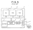
- FIG. 5 A structure of a conventional noncontact IC card is shown in Fig.5.
- a ROM 2 and a RAM 3 are connected through a bus 8 to a CPU 1 which controls operations of the IC card.
- an input-output control circuit 4 Connected to the bus 8 is an input-output control circuit 4 which controls input and output of data to and from an external device and connected to the input-output control circuit 4 through a modem circuit 5 is an antenna 6.
- a battery 7 is contained in the IC card so as to supply electric power to each electric circuit.
- the antenna 6 receives a request signal in the form of electromagnetic wave from the external device, the request signal is input to the CPU 1 through the input-output control circuit 4 after being demodulated in the modem circuit 5.
- the CPU 1 decodes the request signal and produces a predetermined response signal.
- the response signal is input to the modem circuit 5 through the input-output control circuit 4, modulated, and then transmitted to the external device from the antenna 6.
- the present invention is intended to solve the above problem and an object of the present invention is to provide a noncontact IC card which can with certainty receive and process a request signal from an external device while restricting the consumption of the electric power supplied by the battery contained in the IC card.
- a noncontact IC card comprises a data transmit-receive means for transmitting and receiving data to and from outside in a noncontact manner, a detection means for detecting a trigger signal from a signal received by the data transmit-receive means, a data process means connected to the data transmit-receive means for processing the data, a clock generating means for supplying a clock signal to the data process means, an actuating means for actuating the clock generating means in response to the detection of the trigger signal by the detection means, and a battery for supplying electric power to each of the above means.
- a noncontact IC card comprises a data transmit-receive means for transmitting and receiving data to and from outside in a noncontact manner, a detection means for detecting a trigger signal from a signal received by the data transmit-receive means, a data process means connected to the data transmit-receive means for processing the data, a clock generating means for supplying a clock signal to the data process means, an actuating means for actuating the clock generating means in response to the detection of the trigger signal by the detection means, a first stop means for stopping the clock generating means after inputting the clock signal from the clock generating means actuated by the actuating means and executing a predetermined process, and a battery for supplying electric power to each of the above means.
- a noncontact IC card comprises a data transmit-receive means for transmitting and receiving data to and from outside in a noncontact manner, a detection means for detecting a trigger signal from a signal received by the data transmit-receive means, a data process means connected to the data transmit-receive means for processing the data, a clock generating means for supplying a clock signal to the data process means, an actuating means for actuating the clock generating means in response to the detection of the trigger signal by the detection means, a first stop means for stopping the clock generating means after inputting the clock signal from the clock generating means actuated by the actuating means and executing a predetermined process, a measuring means for measuring the time required from when the data process means transmits a response signal through the data transmit-receive means till the data transmit-receive means receives subsequent data, a second stop means for stopping the clock generating means when the required time measured by the measuring means exceeds a predetermined value, and a battery for supplying electric power
- the detection means detects the trigger signal from the received signal
- the clock generating means is actuated by the actuating means and the clock signal is supplied to the data process means.
- the first stop means stops the clock generating means.
- the first stop means stops the clock generating means, and if the time required from when the data process means transmits a response signal till the data transmit-receive means receives subsequent data exceeds a predetermined value, the second stop means stops the clock generating means.
- a noncontact IC card contains an IC 10, and connected to the IC 10 are an antenna circuit 16, a battery 17 and a crystal oscillator 19.
- the IC 10 comprises a CPU 11 connected to a bus 18.
- a ROM 12 for storing a program for controlling operations of the CPU 11, a RAM 13 for storing data and an input-output control circuit 14 for controlling input and output of data from and to an unillustrated external device.
- a timer 20, for dividing and counting an internal clock, and a prescaler 21, for setting an initial value of the timer 20, are connected to the bus 18.
- the input-output control circuit 14 comprises a UART 22 for executing serial asynchronous data transmission, a baud rate generator 23 for setting transmission rate of the UART 22, and a carrier generator 24 for generating a carrier.
- a modem circuit 15 is connected to the input-output control circuit 14 and the antenna circuit 16 is connected to the modem circuit 15.
- the modem circuit 15 comprises a modulation circuit 25 for modulating output of the UART 22 by a carrier, a demodulation circuit 26 for demodulating an input signal from the antenna circuit 16, and output transistors 27 and 28 for driving the antenna circuit 16.
- a clock generating circuit 29 for supplying a clock signal to each circuit in the IC 10 is connected to the CPU 11 and the demodulation circuit 26 in the modem circuit 15.
- the clock generating circuit 29 is connected to the crystal oscillator 19 outside of the IC 10.
- 30 denotes a monitor timer for monitoring runaway of the CPU 11.
- the modem circuit 15 and the antenna circuit 16 constitute a data transmit-receive means
- the CPU 11 constitutes a data process means
- the crystal oscillator 19 and the clock generating circuit 29 constitute a clock generating means
- the timer 20 and the prescaler 21 constitute a measuring means.
- Fig.2 shows an internal structure of the demodulation circuit 26 in the modem circuit 15.
- a first comparator 31 and a second comparator 32, for comparing the amplitude of a detection signal, are respectively connected to an input signal demodulation circuit 33 and a waveform shaping circuit 34.
- a threshold value Vt1 for detecting a request signal is set in the first comparator 31 and a threshold value Vt2 for detecting a trigger signal is set in the second comparator 32.
- These threshold values Vt1 and Vt2 are designed so that the following relation stands up for a level Vs1 of a request signal and a level Vs2 of a trigger signal: Vt1 ⁇ Vs1 ⁇ Vt1 ⁇ Vs2 [1]
- the input signal demodulation circuit 33 is connected to the UART 22 and the waveform shaping circuit 34 is connected to the clock generating circuit 29.
- the second comparator 32 and the waveform shaping circuit 34 constitute a detection means for detecting a trigger signal.
- the internal structure of the clock generating circuit 29 is shown in Fig.3.
- a set terminal S of a second flip flop 37 is connected to an output terminal Q of a first flip flop 35 through an OR circuit 36.
- the output terminal Q of the second flip flop 37 is connected to a reset terminal R of the first flip flop 35 through a NOR circuit 38 while connected to each circuit, such as the CPU 11, in the IC 10 through a NAND circuit 39, 1/2 dividers 40 and 41 and a NAND circuit 42.
- An output of the 1/2 divider 40 is connected to a set terminal S of a third flip flop 46 through a 1/8 divider 43, prescaler 44 and a timer 45, and an output terminal Q of the flip flop 46 is connected to the NAND circuit 42.
- Furthermore, connected to the NAND circuit 39 is the crystal oscillator 19.
- the first and second flip flops 35 and 37, the OR circuit 36, the NOR circuit 38 and the NAND circuit 39 constitute an actuating means and first and second stop means.
- the CPU 11 while waiting to receive a trigger signal from an unillustrated external device, the CPU 11 outputs a STP instruction to the clock generating circuit 29 so that generation of an internal clock is stopped.
- the external device transmits a trigger signal and a subsequent request signal, it is judged in the demodulation circuit 26 in the modem circuit 15 whether the signal received through the antenna circuit 16 is a trigger signal or a request signal.
- the received trigger and request signals respectively have the levels Vs2 and Vs1 shown in the above equation [1]. If a trigger signal is first received, since the level Vs2 of the trigger signal is higher than the threshold value Vt2 of the second comparator 32 shown in Fig.2, a trigger signal pulse is output from the second comparator 32 to the clock generating circuit 29 through the waveform shaping circuit 34.
- the trigger signal pulse is input to a trigger terminal T of the first flip flop 35 shown in Fig.3.
- the flip flop 35 detects a leading edge of the trigger signal pulse and outputs a "H"-level signal from the output terminal Q to the set terminal S of the second flip flop 37 through the OR circuit 36, and then the second flip flop 37 outputs a "H"-level oscillation control signal from the output terminal Q to the NAND circuit 39.
- This causes an oscillation of the crystal oscillator 19 to start and an output of the NAND circuit 39 is divided into 1/4 by the 1/2 dividers 40 and 41 and output as an internal clock from the NAND circuit 42 to each circuit in the IC 10.
- the 1/8 divider 43, the prescaler 44, the timer 45 and the third flip flop 46 operate in order to cause a delay until an oscillation waveform becomes stable, and after a predetermined time has passed since the crystal oscillator 19 started oscillating, the internal clock is output.
- the CPU 11 When the internal clock is thus actuated, the CPU 11 reads a program from the ROM 12 shown in Fig.1 and executes a data process according to a flowchart shown in Fig.4.
- the timer 20 for monitoring receiving of a request signal and the prescaler 21 are initialized in Step S1. Then, a response signal to the trigger signal is transmitted to the external device through the input-output control circuit 14, the modem circuit 15 and the antenna circuit 16 in Step S2.
- the timer 20 and the prescaler 21 is set in an enabled state and the counting of the timer 20 is started in Step S3. It is determined, based on the state of the UART 22, whether or not the data is input through the demodulation circuit 26 in Step S4. If the input of data is confirmed, the content of the received data is read out from the UART 22 and it is judged whether or not the data is a request signal in Step S5.
- the request signal should be at least an 8-bit data string and it is required to be read out for a predetermined length.
- Step 5 If it is judged in Step 5 that the data is a request signal, after an internal process in accordance with the request signal is executed in Step S6, a response signal is transmitted to the external device in Step S7.
- a STP instruction is output to the clock generating circuit 29 in Step S8.
- the STP instruction is input to reset terminals R of the second and third flip flops 37 and 46 shown in Fig.3 so as to make the output terminals Q of the flip flops 37 and 46 at "L"-level. This closes the NAND circuits 39 and 42 and stops the oscillation of the crystal oscillator 19 and the output of the internal clock.
- Step S4 determines whether the data is input to the UART 22. If it is not confirmed in Step S4 that the data is input to the UART 22, or if it is judged in Step S5 that the data is not a request signal, overflow of the timer 20 is checked in Step S9. If the timer 20 does not overflow, Step S4 is repeated and it is judged again whether the data is input to the UART 22. However, if the timer 20 overflows, it is judged that something wrong has happened because the time from when the trigger signal is received until the request signal is received is too long, and the counting of the timer 20 is stopped in Step S10. Then, an STP instruction is executed in Step S8 and the internal clock is stopped.
- the reset signal When a reset signal is input from the reset terminal 47, the reset signal is input to the reset terminal R of the first flip flop 35 through the NOR circuit 38 shown in Fig.3 and to the set terminal S of the second flip flop 37 through the OR circuit 36.
- a trigger prohibition flag signal for prohibiting a trigger can also be input to the NOR circuit 38.
- the reset input to the first flip flop 35 through the NOR circuit 38 is at the "L"-level, the trigger signal pulse is not available.
- the first flip flop 35 detects a leading edge of the trigger signal pulse and outputs an "H"-level signal from the output terminal Q, and therefore, if an extremely long trigger signal pulse is received, that is, a trigger signal is not in a pulse form, but remains at "H"-level, after the CPU 11 executes a STP instruction in response to the overflow of the timer 20, the first flip flop 35 is not set until the trigger signal once reaches the "L"-level. Therefore, it is possible to certainly stop the oscillation of the internal clock.
Landscapes
- Engineering & Computer Science (AREA)
- Physics & Mathematics (AREA)
- General Physics & Mathematics (AREA)
- Theoretical Computer Science (AREA)
- General Engineering & Computer Science (AREA)
- Mechanical Engineering (AREA)
- Computer Networks & Wireless Communication (AREA)
- Computer Hardware Design (AREA)
- Microelectronics & Electronic Packaging (AREA)
- Credit Cards Or The Like (AREA)
Abstract
Description
- The present invention relates to a noncontact integrated circuit (IC) card, and more particularly to a noncontact IC card which is capable of restricting the amount of electric power consumed while waiting to receive signals.
- In recent years, a noncontact IC card, which does not have an external electrode on the surface thereof, has been the most remarkable among the many kinds of IC cards produced. Though the noncontact IC card transmits and receives signals to and from an external device in the same manner as a normal IC card which has an external electrode, the transmission and receiving are performed by using a space transmission medium, such as electromagnetic wave, light, magnetism and so on.
- A structure of a conventional noncontact IC card is shown in Fig.5. A
ROM 2 and aRAM 3 are connected through abus 8 to aCPU 1 which controls operations of the IC card. Connected to thebus 8 is an input-output control circuit 4 which controls input and output of data to and from an external device and connected to the input-output control circuit 4 through amodem circuit 5 is anantenna 6. Furthermore, abattery 7 is contained in the IC card so as to supply electric power to each electric circuit. - In such an IC card, if the
antenna 6 receives a request signal in the form of electromagnetic wave from the external device, the request signal is input to theCPU 1 through the input-output control circuit 4 after being demodulated in themodem circuit 5. TheCPU 1 decodes the request signal and produces a predetermined response signal. The response signal is input to themodem circuit 5 through the input-output control circuit 4, modulated, and then transmitted to the external device from theantenna 6. - However, it is required that the
CPU 1, themodem circuit 5 and so on always be operated on standby so that the IC card receives and processes the request signal from the external device. Therefore, electric power is always being consumed in order to operate theCPU 1, themodem circuit 5 and so on, and this causes a problem in that the electric power supplied by the containedbattery 7 is rapidly consumed. - The present invention is intended to solve the above problem and an object of the present invention is to provide a noncontact IC card which can with certainty receive and process a request signal from an external device while restricting the consumption of the electric power supplied by the battery contained in the IC card.
- A noncontact IC card according to the present invention comprises a data transmit-receive means for transmitting and receiving data to and from outside in a noncontact manner, a detection means for detecting a trigger signal from a signal received by the data transmit-receive means, a data process means connected to the data transmit-receive means for processing the data, a clock generating means for supplying a clock signal to the data process means, an actuating means for actuating the clock generating means in response to the detection of the trigger signal by the detection means, and a battery for supplying electric power to each of the above means.
- A noncontact IC card according to another invention comprises a data transmit-receive means for transmitting and receiving data to and from outside in a noncontact manner, a detection means for detecting a trigger signal from a signal received by the data transmit-receive means, a data process means connected to the data transmit-receive means for processing the data, a clock generating means for supplying a clock signal to the data process means, an actuating means for actuating the clock generating means in response to the detection of the trigger signal by the detection means, a first stop means for stopping the clock generating means after inputting the clock signal from the clock generating means actuated by the actuating means and executing a predetermined process, and a battery for supplying electric power to each of the above means.
- A noncontact IC card according to still another invention comprises a data transmit-receive means for transmitting and receiving data to and from outside in a noncontact manner, a detection means for detecting a trigger signal from a signal received by the data transmit-receive means, a data process means connected to the data transmit-receive means for processing the data, a clock generating means for supplying a clock signal to the data process means, an actuating means for actuating the clock generating means in response to the detection of the trigger signal by the detection means, a first stop means for stopping the clock generating means after inputting the clock signal from the clock generating means actuated by the actuating means and executing a predetermined process, a measuring means for measuring the time required from when the data process means transmits a response signal through the data transmit-receive means till the data transmit-receive means receives subsequent data, a second stop means for stopping the clock generating means when the required time measured by the measuring means exceeds a predetermined value, and a battery for supplying electric power to each of the above means.
- In the noncontact IC card of the present invention, when the detection means detects the trigger signal from the received signal, the clock generating means is actuated by the actuating means and the clock signal is supplied to the data process means.
- In the noncontact IC card of another invention, in addition, after the data process means executes a predetermined process, the first stop means stops the clock generating means.
- Furthermore, in the noncontact IC card of still another invention, after the data process means executes a predetermined process, the first stop means stops the clock generating means, and if the time required from when the data process means transmits a response signal till the data transmit-receive means receives subsequent data exceeds a predetermined value, the second stop means stops the clock generating means.
-
- Fig.1 is a block diagram showing a structure of a noncontact IC card according to an embodiment of the present invention;
- Fig.2 is a block diagram showing an internal structure of a demodulation circuit;
- Fig.3 is a block diagram showing an internal structure of a clock generating circuit;
- Fig.4 is a flowchart showing operations of the embodiment; and
- Fig.5 is a block diagram showing a structure of a conventional noncontact IC card.
- Referring to the accompanying drawings, preferred embodiments of the present invention will be hereinafter described.
- As shown in Fig.1, a noncontact IC card according to an embodiment of the present invention contains an
IC 10, and connected to theIC 10 are anantenna circuit 16, abattery 17 and acrystal oscillator 19. The IC 10 comprises aCPU 11 connected to abus 18. Connected to thebus 18 are aROM 12 for storing a program for controlling operations of theCPU 11, aRAM 13 for storing data and an input-output control circuit 14 for controlling input and output of data from and to an unillustrated external device. Furthermore, atimer 20, for dividing and counting an internal clock, and aprescaler 21, for setting an initial value of thetimer 20, are connected to thebus 18. - The input-
output control circuit 14 comprises aUART 22 for executing serial asynchronous data transmission, abaud rate generator 23 for setting transmission rate of theUART 22, and acarrier generator 24 for generating a carrier. A modem circuit 15 is connected to the input-output control circuit 14 and theantenna circuit 16 is connected to the modem circuit 15. The modem circuit 15 comprises amodulation circuit 25 for modulating output of theUART 22 by a carrier, ademodulation circuit 26 for demodulating an input signal from theantenna circuit 16, andoutput transistors 27 and 28 for driving theantenna circuit 16. - Furthermore, a
clock generating circuit 29 for supplying a clock signal to each circuit in theIC 10 is connected to theCPU 11 and thedemodulation circuit 26 in the modem circuit 15. Theclock generating circuit 29 is connected to thecrystal oscillator 19 outside of theIC 10. 30 denotes a monitor timer for monitoring runaway of theCPU 11. - The modem circuit 15 and the
antenna circuit 16 constitute a data transmit-receive means, theCPU 11 constitutes a data process means, thecrystal oscillator 19 and theclock generating circuit 29 constitute a clock generating means, and thetimer 20 and theprescaler 21 constitute a measuring means. - Fig.2 shows an internal structure of the
demodulation circuit 26 in the modem circuit 15. Afirst comparator 31 and asecond comparator 32, for comparing the amplitude of a detection signal, are respectively connected to an input signal demodulation circuit 33 and awaveform shaping circuit 34. A threshold value Vt₁ for detecting a request signal is set in thefirst comparator 31 and a threshold value Vt₂ for detecting a trigger signal is set in thesecond comparator 32. These threshold values Vt₁ and Vt₂ are designed so that the following relation stands up for a level Vs₁ of a request signal and a level Vs₂ of a trigger signal:

- Furthermore, the input signal demodulation circuit 33 is connected to the
UART 22 and thewaveform shaping circuit 34 is connected to theclock generating circuit 29. - The
second comparator 32 and thewaveform shaping circuit 34 constitute a detection means for detecting a trigger signal. - The internal structure of the
clock generating circuit 29 is shown in Fig.3. A set terminal S of asecond flip flop 37 is connected to an output terminal Q of afirst flip flop 35 through anOR circuit 36. The output terminal Q of thesecond flip flop 37 is connected to a reset terminal R of thefirst flip flop 35 through aNOR circuit 38 while connected to each circuit, such as theCPU 11, in theIC 10 through aNAND circuit dividers NAND circuit 42. An output of the 1/2divider 40 is connected to a set terminal S of athird flip flop 46 through a 1/8divider 43,prescaler 44 and atimer 45, and an output terminal Q of theflip flop 46 is connected to theNAND circuit 42. Furthermore, connected to theNAND circuit 39 is thecrystal oscillator 19. - The first and
second flip flops OR circuit 36, theNOR circuit 38 and theNAND circuit 39 constitute an actuating means and first and second stop means. - Next, operations of the embodiment will be explained. First, as shown in Fig.1, while waiting to receive a trigger signal from an unillustrated external device, the
CPU 11 outputs a STP instruction to theclock generating circuit 29 so that generation of an internal clock is stopped. - When the external device transmits a trigger signal and a subsequent request signal, it is judged in the
demodulation circuit 26 in the modem circuit 15 whether the signal received through theantenna circuit 16 is a trigger signal or a request signal. The received trigger and request signals respectively have the levels Vs₂ and Vs₁ shown in the above equation [1]. If a trigger signal is first received, since the level Vs₂ of the trigger signal is higher than the threshold value Vt₂ of thesecond comparator 32 shown in Fig.2, a trigger signal pulse is output from thesecond comparator 32 to theclock generating circuit 29 through thewaveform shaping circuit 34. - The trigger signal pulse is input to a trigger terminal T of the
first flip flop 35 shown in Fig.3. Theflip flop 35 detects a leading edge of the trigger signal pulse and outputs a "H"-level signal from the output terminal Q to the set terminal S of thesecond flip flop 37 through theOR circuit 36, and then thesecond flip flop 37 outputs a "H"-level oscillation control signal from the output terminal Q to theNAND circuit 39. This causes an oscillation of thecrystal oscillator 19 to start and an output of theNAND circuit 39 is divided into 1/4 by the 1/2dividers NAND circuit 42 to each circuit in theIC 10. In actuality, the 1/8divider 43, theprescaler 44, thetimer 45 and thethird flip flop 46 operate in order to cause a delay until an oscillation waveform becomes stable, and after a predetermined time has passed since thecrystal oscillator 19 started oscillating, the internal clock is output. - When the internal clock is thus actuated, the
CPU 11 reads a program from theROM 12 shown in Fig.1 and executes a data process according to a flowchart shown in Fig.4. Thetimer 20 for monitoring receiving of a request signal and theprescaler 21 are initialized in Step S1. Then, a response signal to the trigger signal is transmitted to the external device through the input-output control circuit 14, the modem circuit 15 and theantenna circuit 16 in Step S2. - After that, the
timer 20 and theprescaler 21 is set in an enabled state and the counting of thetimer 20 is started in Step S3. It is determined, based on the state of theUART 22, whether or not the data is input through thedemodulation circuit 26 in Step S4. If the input of data is confirmed, the content of the received data is read out from theUART 22 and it is judged whether or not the data is a request signal in Step S5. The request signal should be at least an 8-bit data string and it is required to be read out for a predetermined length. - If it is judged in
Step 5 that the data is a request signal, after an internal process in accordance with the request signal is executed in Step S6, a response signal is transmitted to the external device in Step S7. When the transmission is completed, a STP instruction is output to theclock generating circuit 29 in Step S8. The STP instruction is input to reset terminals R of the second andthird flip flops flip flops NAND circuits crystal oscillator 19 and the output of the internal clock. - On the other hand, if it is not confirmed in Step S4 that the data is input to the
UART 22, or if it is judged in Step S5 that the data is not a request signal, overflow of thetimer 20 is checked in Step S9. If thetimer 20 does not overflow, Step S4 is repeated and it is judged again whether the data is input to theUART 22. However, if thetimer 20 overflows, it is judged that something wrong has happened because the time from when the trigger signal is received until the request signal is received is too long, and the counting of thetimer 20 is stopped in Step S10. Then, an STP instruction is executed in Step S8 and the internal clock is stopped. - After this, in order to actuate again the internal clock and operate the
CPU 11, it is necessary to receive a trigger signal from the external device or input a reset signal from thereset terminal 47 of theIC 10 shown in Fig.1 to theclock generating circuit 29 through theOR circuit 48. - When a reset signal is input from the
reset terminal 47, the reset signal is input to the reset terminal R of thefirst flip flop 35 through the NORcircuit 38 shown in Fig.3 and to the set terminal S of thesecond flip flop 37 through theOR circuit 36. - Furthermore, besides a reset signal and an oscillation control signal which is an output of the output terminal Q of the
second flip flop 37, a trigger prohibition flag signal for prohibiting a trigger can also be input to the NORcircuit 38. When the reset input to thefirst flip flop 35 through the NORcircuit 38 is at the "L"-level, the trigger signal pulse is not available. - The
first flip flop 35 detects a leading edge of the trigger signal pulse and outputs an "H"-level signal from the output terminal Q, and therefore, if an extremely long trigger signal pulse is received, that is, a trigger signal is not in a pulse form, but remains at "H"-level, after theCPU 11 executes a STP instruction in response to the overflow of thetimer 20, thefirst flip flop 35 is not set until the trigger signal once reaches the "L"-level. Therefore, it is possible to certainly stop the oscillation of the internal clock.
Claims (21)
- A noncontact IC card, comprising:
data transmit-receive means for transmitting and receiving data to and from outside in a noncontact manner;
detection means for detecting a trigger signal from a signal received by said data transmit-receive means;
data process means connected to said data transmit-receive means for processing data;
clock generating means for supplying a clock signal to said data process means;
actuating means for actuating said clock generating means when said detection means detects a trigger signal; and
a battery for supplying electric power to each of said means. - A noncontact IC card as claimed in claim 1, wherein said data transmit-receive means comprises an antenna circuit and a modulation circuit and a demodulation circuit which are respectively connected to said antenna circuit.
- A noncontact IC card as claimed in claim 2, wherein said detection means is mounted in said demodulation circuit.
- A noncontact IC card as claimed in claim 3, wherein said detection means discriminates between a trigger signal and a data signal in a signal which said data transmit-receive means receives.
- A noncontact IC card as claimed in claim 4, wherein said detection means discriminates between a trigger signal and a data signal based on difference in amplitude between said signals.
- A noncontact IC card as claimed in claim 1, further comprising a data memory means connected to said data process means for storing data.
- A noncontact IC card, comprising:
data transmit-receive means for transmitting and receiving data to and from outside in a noncontact manner;
detection means for detecting a trigger signal from a signal received by said data transmit-receive means;
data process means connected to said data transmit-receive means for processing data;
clock generating means for supplying a clock signal to said data process means;
actuating means for actuating said clock generating means when said detection means detects a trigger signal;
first stop means for stopping said clock generating means after said data process means inputs a clock signal from said clock generating means actuated by said actuating means and executes a predetermined process; and
a battery for supplying electric power to each of said means. - A noncontact IC card as claimed in claim 7, wherein said data transmit-receive means includes an antenna circuit and a modulation circuit and a demodulation circuit which are respectively connected to said antenna circuit.
- A noncontact IC card as claimed in claim 8, wherein said detection means is mounted in said demodulation circuit.
- A noncontact IC card as claimed in claim 9, wherein said detection means discriminates between a trigger signal and a data signal in a signal which said data transmit-receive means receives.
- A noncontact IC card as claimed in claim 10, wherein said detection means discriminates between a trigger signal and a data signal based on difference in amplitude between said signals.
- A noncontact IC card as claimed in claim 7, further comprising a data memory means connected to said data process means for storing data.
- A noncontact IC card as claimed in claim 7, wherein said first stop means is operated by an instruction from said data process means.
- A noncontact IC card, comprising:
data transmit-receive means for transmitting and receiving data to and from outside in a noncontact manner;
detection means for detecting a leading edge of a trigger signal from a signal received by said data transmit-receive means;
data process means connected to said data transmit-receive means for processing data and transmitting a response signal when said data transmit-receive means receives a trigger signal;
clock generating means for supplying a clock signal to said data process means;
actuating means for actuating said clock generating means when said detection means detects a trigger signal;
first stop means for stopping said clock generating means after said data process means inputs a clock signal from said clock generating means actuated by said actuating means and executes a predetermined process;
measuring means for measuring the time required from when said data process means transmits said response signal through said data transmit-receive means until said data transmit-receive means receives subsequent data;
second stop means for stopping said clock generating means when the required time measured by said measuring means exceeds a predetermined value; and
a battery for supplying electric power to each of said means. - A noncontact IC card as claimed in claim 14, wherein said data transmit-receive means comprises an antenna circuit and a modulation circuit and a demodulation circuit which are respectively connected to said antenna circuit.
- A noncontact IC card as claimed in claim 15, wherein said detection means is mounted in said demodulation circuit.
- A noncontact IC card as claimed in claim 16, wherein said detection means discriminates between a trigger signal and a data signal in a signal which said data transmit-receive means receives.
- A noncontact IC card as claimed in claim 17, wherein said detection means discriminates between a trigger signal and a data signal based on difference in amplitude between said signals.
- A noncontact IC card as claimed in claim 14, further comprising a data memory means connected to said data process means for storing data.
- A noncontact IC card as claimed in claim 14, wherein said first stop means is operated by an instruction from said data process means.
- A noncontact IC card substantially as hereinbefore described with reference to the embodiments described herein and Figures 1 to 4 of of the accompanying drawings.
Applications Claiming Priority (2)
| Application Number | Priority Date | Filing Date | Title |
|---|---|---|---|
| JP59928/90 | 1990-03-13 | ||
| JP2059928A JP2645163B2 (en) | 1990-03-13 | 1990-03-13 | Non-contact IC card |
Publications (3)
| Publication Number | Publication Date |
|---|---|
| EP0446519A2 true EP0446519A2 (en) | 1991-09-18 |
| EP0446519A3 EP0446519A3 (en) | 1993-01-13 |
| EP0446519B1 EP0446519B1 (en) | 1994-12-14 |
Family
ID=13127281
Family Applications (1)
| Application Number | Title | Priority Date | Filing Date |
|---|---|---|---|
| EP90311336A Expired - Lifetime EP0446519B1 (en) | 1990-03-13 | 1990-10-16 | Noncontact integrated circuit card |
Country Status (4)
| Country | Link |
|---|---|
| US (1) | US5182442A (en) |
| EP (1) | EP0446519B1 (en) |
| JP (1) | JP2645163B2 (en) |
| DE (1) | DE69015154T2 (en) |
Cited By (9)
| Publication number | Priority date | Publication date | Assignee | Title |
|---|---|---|---|---|
| EP0569131A3 (en) * | 1992-04-07 | 1993-12-15 | Mitsubishi Electric Corp | Ic card |
| EP0575013A1 (en) * | 1992-06-18 | 1993-12-22 | N.V. Nederlandsche Apparatenfabriek NEDAP | System for the contactless exchange of data, and responder for use in such a system |
| EP0605751A1 (en) * | 1992-12-08 | 1994-07-13 | Mitsubishi Denki Kabushiki Kaisha | Uart and system using the same |
| GB2245725B (en) * | 1990-07-03 | 1994-08-31 | Mitsubishi Electric Corp | Non-contact IC card |
| EP0666529A1 (en) * | 1994-02-02 | 1995-08-09 | Advanced Micro Devices, Inc. | Power management in an asynchronus receiver/transmitter |
| EP0609453A4 (en) * | 1992-06-25 | 1996-11-06 | Nippon Denso Co | Mobile object identification device. |
| EP1564630A1 (en) * | 2004-02-04 | 2005-08-17 | Sharp Kabushiki Kaisha | IC card with built-in coprocessor for auxiliary arithmetic, and control method thereof |
| KR100708010B1 (en) * | 1999-11-10 | 2007-04-16 | 어드밴스드 마이크로 디바이시즈, 인코포레이티드 | Storage buffers that forward data based on indexes and optional path matching |
| EP1986325A3 (en) * | 2007-04-26 | 2009-10-07 | Semiconductor Energy Laboratory Co., Ltd. | Semiconductor device and driving method thereof |
Families Citing this family (28)
| Publication number | Priority date | Publication date | Assignee | Title |
|---|---|---|---|---|
| WO1992021104A1 (en) * | 1991-05-22 | 1992-11-26 | Kyodo Printing Co., Ltd. | Non-contact type ic card |
| JPH0528330A (en) * | 1991-07-24 | 1993-02-05 | Mitsubishi Electric Corp | Non-contact type portable carrier and its initialization method |
| JP2713529B2 (en) * | 1992-08-21 | 1998-02-16 | 三菱電機株式会社 | Signal receiving coil and non-contact IC card using the same |
| US5426483A (en) * | 1992-09-14 | 1995-06-20 | Nikon Corporation | Camera with a line of sight detecting device |
| US5983363A (en) | 1992-11-20 | 1999-11-09 | Micron Communications, Inc. | In-sheet transceiver testing |
| US6058497A (en) * | 1992-11-20 | 2000-05-02 | Micron Technology, Inc. | Testing and burn-in of IC chips using radio frequency transmission |
| JPH0721336A (en) * | 1993-07-05 | 1995-01-24 | Mitsubishi Electric Corp | Contact type mobile device and non-contact type mobile device |
| US5557516A (en) * | 1994-02-04 | 1996-09-17 | Mastercard International | System and method for conducting cashless transactions |
| US5451763A (en) * | 1994-07-05 | 1995-09-19 | Alto Corporation | Personal medical IC card and read/write unit |
| JPH0830749A (en) * | 1994-07-13 | 1996-02-02 | Mitsubishi Electric Corp | Non-contact IC card |
| US5834747A (en) * | 1994-11-04 | 1998-11-10 | Pixel Instruments | Universal credit card apparatus and method |
| CN1107922C (en) * | 1995-06-16 | 2003-05-07 | 罗姆股份有限公司 | Semiconductor device, IC card utilzing the same and communication system |
| JPH0962808A (en) * | 1995-08-25 | 1997-03-07 | Mitsubishi Electric Corp | Contactless IC card and contactless IC card system |
| US5971282A (en) * | 1995-09-26 | 1999-10-26 | Intel Corporation | Personal token card with sensor |
| US5704046A (en) * | 1996-05-30 | 1997-12-30 | Mastercard International Inc. | System and method for conducting cashless transactions |
| SG54559A1 (en) * | 1996-09-13 | 1998-11-16 | Hitachi Ltd | Power transmission system ic card and information communication system using ic card |
| JP3392016B2 (en) * | 1996-09-13 | 2003-03-31 | 株式会社日立製作所 | Power transmission system and power transmission and information communication system |
| US5812942A (en) * | 1996-09-24 | 1998-09-22 | Motorola, Inc. | Balanced differential radio receiver and method of operation |
| US5815020A (en) * | 1996-09-24 | 1998-09-29 | Motorola, Inc. | Balance differential receiver |
| US6119255A (en) | 1998-01-21 | 2000-09-12 | Micron Technology, Inc. | Testing system for evaluating integrated circuits, a burn-in testing system, and a method for testing an integrated circuit |
| FR2774195A1 (en) * | 1998-01-27 | 1999-07-30 | Gemplus Card Int | Microprocessor smart card with wired communication circuit |
| IL123949A (en) * | 1998-04-03 | 2001-07-24 | On Track Innovations Ltd | Data transaction card having extended range |
| EP1046125B1 (en) * | 1998-09-30 | 2008-12-24 | Nxp B.V. | Data carrier |
| JP3613546B2 (en) * | 1999-04-09 | 2005-01-26 | ローム株式会社 | Data processing system, data processing apparatus, and data processing method |
| US6714121B1 (en) * | 1999-08-09 | 2004-03-30 | Micron Technology, Inc. | RFID material tracking method and apparatus |
| JP2001266094A (en) * | 2000-03-15 | 2001-09-28 | Toshiba Corp | Non-contact communication device and control method of non-contact communication device |
| US7463682B2 (en) * | 2002-07-31 | 2008-12-09 | Institute Of Process Engineering, Chinese Academy Of Sciences | Coding method for binary digits coding and its circuit for digits transmission |
| JP3929887B2 (en) * | 2002-12-25 | 2007-06-13 | 株式会社東芝 | Semiconductor integrated circuit, semiconductor integrated circuit module, and information device |
Family Cites Families (15)
| Publication number | Priority date | Publication date | Assignee | Title |
|---|---|---|---|---|
| US4203153A (en) * | 1978-04-12 | 1980-05-13 | Diebold, Incorporated | Circuit for reducing power consumption in battery operated microprocessor based systems |
| JPS59212949A (en) * | 1983-05-18 | 1984-12-01 | Dainippon Printing Co Ltd | Ic card and its processing method and device |
| JPH0682405B2 (en) * | 1986-01-14 | 1994-10-19 | カシオ計算機株式会社 | Test program start method |
| JP2658018B2 (en) * | 1986-03-12 | 1997-09-30 | カシオ計算機株式会社 | Power supply control method |
| JPS62237592A (en) * | 1986-04-08 | 1987-10-17 | Casio Comput Co Ltd | Clock switching method in IC card |
| GB2194082A (en) * | 1986-08-18 | 1988-02-24 | Philips Nv | Data processing apparatus with energy saving clocking device |
| US4766294A (en) * | 1986-08-29 | 1988-08-23 | Kabushiki Kaisha Toshiba | Portable medium |
| FR2604808A1 (en) * | 1986-10-02 | 1988-04-08 | Bazin Gerard | Self-contained electronic identification device which can be remotely interrogated |
| JPS63157253A (en) * | 1986-12-22 | 1988-06-30 | Toshiba Corp | Portable medium |
| JPS63246203A (en) * | 1987-03-31 | 1988-10-13 | 株式会社 神戸機械製作所 | Molding technique by lathe for pottery |
| US4868376A (en) * | 1987-05-15 | 1989-09-19 | Smartcard International Inc. | Intelligent portable interactive personal data system |
| JPS6488764A (en) * | 1987-09-30 | 1989-04-03 | Toshiba Corp | Portable electronic equipment |
| JPH01191282A (en) * | 1988-01-26 | 1989-08-01 | Matsushita Electric Works Ltd | Non-contact id card system and identifying device |
| DK174975B1 (en) * | 1988-05-06 | 2004-04-05 | Toppan Printing Co Ltd | Integrated circuit board |
| JPH023882A (en) * | 1988-06-16 | 1990-01-09 | Star Micronics Co Ltd | Ic card |
-
1990
- 1990-03-13 JP JP2059928A patent/JP2645163B2/en not_active Expired - Lifetime
- 1990-08-09 US US07/564,851 patent/US5182442A/en not_active Expired - Lifetime
- 1990-10-16 DE DE69015154T patent/DE69015154T2/en not_active Expired - Fee Related
- 1990-10-16 EP EP90311336A patent/EP0446519B1/en not_active Expired - Lifetime
Cited By (16)
| Publication number | Priority date | Publication date | Assignee | Title |
|---|---|---|---|---|
| GB2245725B (en) * | 1990-07-03 | 1994-08-31 | Mitsubishi Electric Corp | Non-contact IC card |
| EP0569131A3 (en) * | 1992-04-07 | 1993-12-15 | Mitsubishi Electric Corp | Ic card |
| US5365047A (en) * | 1992-04-07 | 1994-11-15 | Mitsubishi Denki Kabushiki Kaisha | IC card with clock signal input control |
| EP0575013A1 (en) * | 1992-06-18 | 1993-12-22 | N.V. Nederlandsche Apparatenfabriek NEDAP | System for the contactless exchange of data, and responder for use in such a system |
| US5426667A (en) * | 1992-06-18 | 1995-06-20 | N.V. Nederlandsche Apparatenfabriek Nedap | System for the contactless exchange of data, and responder for use in such a system |
| EP1249712A1 (en) * | 1992-06-25 | 2002-10-16 | Denso Corporation | Mobile object identification system |
| EP0609453A4 (en) * | 1992-06-25 | 1996-11-06 | Nippon Denso Co | Mobile object identification device. |
| EP0605751A1 (en) * | 1992-12-08 | 1994-07-13 | Mitsubishi Denki Kabushiki Kaisha | Uart and system using the same |
| US5661751A (en) * | 1994-02-02 | 1997-08-26 | Advanced Micro Devices | System and technique for power management of a universal asynchronous receiver/transmitter by automatic clock gating |
| EP0666529A1 (en) * | 1994-02-02 | 1995-08-09 | Advanced Micro Devices, Inc. | Power management in an asynchronus receiver/transmitter |
| KR100708010B1 (en) * | 1999-11-10 | 2007-04-16 | 어드밴스드 마이크로 디바이시즈, 인코포레이티드 | Storage buffers that forward data based on indexes and optional path matching |
| EP1564630A1 (en) * | 2004-02-04 | 2005-08-17 | Sharp Kabushiki Kaisha | IC card with built-in coprocessor for auxiliary arithmetic, and control method thereof |
| US7364083B2 (en) | 2004-02-04 | 2008-04-29 | Sharp Kabushiki Kaisha | IC card with built-in coprocessor for auxiliary arithmetic, and control method thereof |
| CN100465991C (en) * | 2004-02-04 | 2009-03-04 | 夏普株式会社 | IC card with built-in coprocessor for auxiliary operation and control method thereof |
| EP1986325A3 (en) * | 2007-04-26 | 2009-10-07 | Semiconductor Energy Laboratory Co., Ltd. | Semiconductor device and driving method thereof |
| US7667549B2 (en) | 2007-04-26 | 2010-02-23 | Semiconductor Energy Laboratory Co., Ltd. | Semiconductor device and driving method thereof |
Also Published As
| Publication number | Publication date |
|---|---|
| JP2645163B2 (en) | 1997-08-25 |
| US5182442A (en) | 1993-01-26 |
| DE69015154T2 (en) | 1995-08-03 |
| EP0446519A3 (en) | 1993-01-13 |
| DE69015154D1 (en) | 1995-01-26 |
| JPH03262089A (en) | 1991-11-21 |
| EP0446519B1 (en) | 1994-12-14 |
Similar Documents
| Publication | Publication Date | Title |
|---|---|---|
| EP0446519B1 (en) | Noncontact integrated circuit card | |
| US5382778A (en) | Non-contact IC card | |
| US5220158A (en) | Non-contact ic card and method of using the same | |
| EP0587115B1 (en) | Communication system | |
| US5274221A (en) | Non-contact integrated circuit card | |
| US4477807A (en) | Radio pager with display device | |
| JP2822624B2 (en) | Non-contact IC card | |
| EP0569131B1 (en) | IC card | |
| EP0170716A1 (en) | Information medium | |
| EP0446958A2 (en) | Single-chip microcumputer with clocksignal switching function | |
| JP4558259B2 (en) | Combination IC card | |
| US20100176202A1 (en) | Noncontact data carrier | |
| JPH0454581A (en) | Non-contact card | |
| US6125452A (en) | Terminal unit for IC card using plural protocols and control method therefor | |
| EP0866414A2 (en) | Non-contact type portable device | |
| EP0762307A2 (en) | IC card reader | |
| CN111818480B (en) | OBU (on-board unit) testing method and system | |
| EP1198783B1 (en) | Data carrier having means for synchronization with a received data stream | |
| JPH09130999A (en) | Semiconductor integrated circuit device and battery-less RFID using the same | |
| EP1003046A1 (en) | Voltage detecting circuit | |
| JP3205260B2 (en) | Non-contact data transmission / reception method and device | |
| JP3511046B2 (en) | IC card | |
| JPH08315092A (en) | Non-contact ic card | |
| JPH05266272A (en) | Contactless IC card reset method | |
| JPH0398188A (en) | Ic card |
Legal Events
| Date | Code | Title | Description |
|---|---|---|---|
| PUAI | Public reference made under article 153(3) epc to a published international application that has entered the european phase |
Free format text: ORIGINAL CODE: 0009012 |
|
| 17P | Request for examination filed |
Effective date: 19910102 |
|
| AK | Designated contracting states |
Kind code of ref document: A2 Designated state(s): DE FR GB |
|
| PUAL | Search report despatched |
Free format text: ORIGINAL CODE: 0009013 |
|
| AK | Designated contracting states |
Kind code of ref document: A3 Designated state(s): DE FR GB |
|
| 17Q | First examination report despatched |
Effective date: 19930826 |
|
| GRAA | (expected) grant |
Free format text: ORIGINAL CODE: 0009210 |
|
| AK | Designated contracting states |
Kind code of ref document: B1 Designated state(s): DE FR GB |
|
| REF | Corresponds to: |
Ref document number: 69015154 Country of ref document: DE Date of ref document: 19950126 |
|
| REG | Reference to a national code |
Ref country code: GB Ref legal event code: 727 |
|
| ET | Fr: translation filed | ||
| REG | Reference to a national code |
Ref country code: GB Ref legal event code: 727A |
|
| REG | Reference to a national code |
Ref country code: GB Ref legal event code: 727B |
|
| PLBE | No opposition filed within time limit |
Free format text: ORIGINAL CODE: 0009261 |
|
| STAA | Information on the status of an ep patent application or granted ep patent |
Free format text: STATUS: NO OPPOSITION FILED WITHIN TIME LIMIT |
|
| REG | Reference to a national code |
Ref country code: GB Ref legal event code: SP |
|
| 26N | No opposition filed | ||
| REG | Reference to a national code |
Ref country code: GB Ref legal event code: 746 Effective date: 19951106 |
|
| REG | Reference to a national code |
Ref country code: FR Ref legal event code: D6 |
|
| REG | Reference to a national code |
Ref country code: GB Ref legal event code: IF02 |
|
| PGFP | Annual fee paid to national office [announced via postgrant information from national office to epo] |
Ref country code: DE Payment date: 20081014 Year of fee payment: 19 |
|
| PGFP | Annual fee paid to national office [announced via postgrant information from national office to epo] |
Ref country code: FR Payment date: 20081014 Year of fee payment: 19 |
|
| PGFP | Annual fee paid to national office [announced via postgrant information from national office to epo] |
Ref country code: GB Payment date: 20081015 Year of fee payment: 19 |
|
| REG | Reference to a national code |
Ref country code: FR Ref legal event code: ST Effective date: 20100630 |
|
| PG25 | Lapsed in a contracting state [announced via postgrant information from national office to epo] |
Ref country code: FR Free format text: LAPSE BECAUSE OF NON-PAYMENT OF DUE FEES Effective date: 20091102 Ref country code: DE Free format text: LAPSE BECAUSE OF NON-PAYMENT OF DUE FEES Effective date: 20100501 |
|
| PG25 | Lapsed in a contracting state [announced via postgrant information from national office to epo] |
Ref country code: GB Free format text: LAPSE BECAUSE OF NON-PAYMENT OF DUE FEES Effective date: 20091016 |