EP0446596A2 - Procédé PCVD pour la production de substrats sous la forme de calotte pourvus à l'intérieur et/ou à l'extérieur de revêtements diélectriques et/ou métalliques - Google Patents
Procédé PCVD pour la production de substrats sous la forme de calotte pourvus à l'intérieur et/ou à l'extérieur de revêtements diélectriques et/ou métalliques Download PDFInfo
- Publication number
- EP0446596A2 EP0446596A2 EP91101392A EP91101392A EP0446596A2 EP 0446596 A2 EP0446596 A2 EP 0446596A2 EP 91101392 A EP91101392 A EP 91101392A EP 91101392 A EP91101392 A EP 91101392A EP 0446596 A2 EP0446596 A2 EP 0446596A2
- Authority
- EP
- European Patent Office
- Prior art keywords
- gas
- displacement body
- coating
- layer
- coated
- Prior art date
- Legal status (The legal status is an assumption and is not a legal conclusion. Google has not performed a legal analysis and makes no representation as to the accuracy of the status listed.)
- Granted
Links
Images

Classifications
-
- C—CHEMISTRY; METALLURGY
- C23—COATING METALLIC MATERIAL; COATING MATERIAL WITH METALLIC MATERIAL; CHEMICAL SURFACE TREATMENT; DIFFUSION TREATMENT OF METALLIC MATERIAL; COATING BY VACUUM EVAPORATION, BY SPUTTERING, BY ION IMPLANTATION OR BY CHEMICAL VAPOUR DEPOSITION, IN GENERAL; INHIBITING CORROSION OF METALLIC MATERIAL OR INCRUSTATION IN GENERAL
- C23C—COATING METALLIC MATERIAL; COATING MATERIAL WITH METALLIC MATERIAL; SURFACE TREATMENT OF METALLIC MATERIAL BY DIFFUSION INTO THE SURFACE, BY CHEMICAL CONVERSION OR SUBSTITUTION; COATING BY VACUUM EVAPORATION, BY SPUTTERING, BY ION IMPLANTATION OR BY CHEMICAL VAPOUR DEPOSITION, IN GENERAL
- C23C16/00—Chemical coating by decomposition of gaseous compounds, without leaving reaction products of surface material in the coating, i.e. chemical vapour deposition [CVD] processes
- C23C16/44—Chemical coating by decomposition of gaseous compounds, without leaving reaction products of surface material in the coating, i.e. chemical vapour deposition [CVD] processes characterised by the method of coating
- C23C16/455—Chemical coating by decomposition of gaseous compounds, without leaving reaction products of surface material in the coating, i.e. chemical vapour deposition [CVD] processes characterised by the method of coating characterised by the method used for introducing gases into reaction chamber or for modifying gas flows in reaction chamber
- C23C16/45517—Confinement of gases to vicinity of substrate
-
- C—CHEMISTRY; METALLURGY
- C03—GLASS; MINERAL OR SLAG WOOL
- C03C—CHEMICAL COMPOSITION OF GLASSES, GLAZES OR VITREOUS ENAMELS; SURFACE TREATMENT OF GLASS; SURFACE TREATMENT OF FIBRES OR FILAMENTS MADE FROM GLASS, MINERALS OR SLAGS; JOINING GLASS TO GLASS OR OTHER MATERIALS
- C03C17/00—Surface treatment of glass, not in the form of fibres or filaments, by coating
- C03C17/001—General methods for coating; Devices therefor
-
- C—CHEMISTRY; METALLURGY
- C23—COATING METALLIC MATERIAL; COATING MATERIAL WITH METALLIC MATERIAL; CHEMICAL SURFACE TREATMENT; DIFFUSION TREATMENT OF METALLIC MATERIAL; COATING BY VACUUM EVAPORATION, BY SPUTTERING, BY ION IMPLANTATION OR BY CHEMICAL VAPOUR DEPOSITION, IN GENERAL; INHIBITING CORROSION OF METALLIC MATERIAL OR INCRUSTATION IN GENERAL
- C23C—COATING METALLIC MATERIAL; COATING MATERIAL WITH METALLIC MATERIAL; SURFACE TREATMENT OF METALLIC MATERIAL BY DIFFUSION INTO THE SURFACE, BY CHEMICAL CONVERSION OR SUBSTITUTION; COATING BY VACUUM EVAPORATION, BY SPUTTERING, BY ION IMPLANTATION OR BY CHEMICAL VAPOUR DEPOSITION, IN GENERAL
- C23C16/00—Chemical coating by decomposition of gaseous compounds, without leaving reaction products of surface material in the coating, i.e. chemical vapour deposition [CVD] processes
- C23C16/04—Coating on selected surface areas, e.g. using masks
- C23C16/045—Coating cavities or hollow spaces, e.g. interior of tubes; Infiltration of porous substrates
-
- C—CHEMISTRY; METALLURGY
- C23—COATING METALLIC MATERIAL; COATING MATERIAL WITH METALLIC MATERIAL; CHEMICAL SURFACE TREATMENT; DIFFUSION TREATMENT OF METALLIC MATERIAL; COATING BY VACUUM EVAPORATION, BY SPUTTERING, BY ION IMPLANTATION OR BY CHEMICAL VAPOUR DEPOSITION, IN GENERAL; INHIBITING CORROSION OF METALLIC MATERIAL OR INCRUSTATION IN GENERAL
- C23C—COATING METALLIC MATERIAL; COATING MATERIAL WITH METALLIC MATERIAL; SURFACE TREATMENT OF METALLIC MATERIAL BY DIFFUSION INTO THE SURFACE, BY CHEMICAL CONVERSION OR SUBSTITUTION; COATING BY VACUUM EVAPORATION, BY SPUTTERING, BY ION IMPLANTATION OR BY CHEMICAL VAPOUR DEPOSITION, IN GENERAL
- C23C16/00—Chemical coating by decomposition of gaseous compounds, without leaving reaction products of surface material in the coating, i.e. chemical vapour deposition [CVD] processes
- C23C16/44—Chemical coating by decomposition of gaseous compounds, without leaving reaction products of surface material in the coating, i.e. chemical vapour deposition [CVD] processes characterised by the method of coating
- C23C16/455—Chemical coating by decomposition of gaseous compounds, without leaving reaction products of surface material in the coating, i.e. chemical vapour deposition [CVD] processes characterised by the method of coating characterised by the method used for introducing gases into reaction chamber or for modifying gas flows in reaction chamber
- C23C16/45563—Gas nozzles
Definitions
- the invention relates to a plasma CVD method for producing an approximately spherical substrate provided on the inner and / or outer surface with a dielectric and / or metallic layer system, in particular a reflector with an internal dielectric cold light mirror coating, and a device for carrying out the method.
- reflectors consist of curved, usually dome-shaped glass substrates with an internal reflective coating.
- the reflection coating can consist of a metallic layer or, if a special spectral course of the reflectance is desired, of a dielectric layer system. So you can e.g. so-called cold light mirrors, such as Manufacture dental mirrors, which only have a high degree of reflection in the visible spectral range, but are transparent to heat radiation.
- Dielectric layer systems with a selective spectral reflectivity generally exist. from alternating layers of high and low refractive index. How to build up such layer systems in detail, i.e. how many pairs of layers are to be arranged one above the other and how the layer thicknesses are to be dimensioned to achieve a desired optical effect is known to the person skilled in the art and e.g. in H.A. Macleod, Thin Film Optical Filters, A. Hilger Ltd., London.
- the dielectric layer systems are usually produced using high vacuum processes, such as high vacuum evaporation, cathode sputtering or electron beam sputtering applied to the substrates.
- high vacuum processes such as high vacuum evaporation, cathode sputtering or electron beam sputtering applied to the substrates.
- a "gas spreading method” is generally used (K. Steinfelder et al., Vacuum Technology 28 (1979), p. 48).
- the vaporization is carried out under increased pressure (about 10 ⁇ 3mbar) of an additional gas, which has the task of interrupting the linear movement of the vapor particles from the vapor deposition source to the substrate by multiple impacts with the additional gas, so that no preferred direction in the movement of the vapor particles more exists.
- so-called "soft” layer systems made of ZnS / MgF2 layer pairs can be produced, but which are sensitive to touch, and so-called “semi-hard” layer systems made of Zns / SiO2 and ZnS / Al2O3 layer pairs, which are non-slip but mechanically are resilient.
- SiO2 / TiO2 layer systems can be produced which meet high requirements with regard to their mechanical, chemical and thermal resilience and are therefore usually referred to as so-called "hard” layer systems. Due to the more difficult production (e.g. complicated substrate movement, substrate heating), these layer systems on highly curved substrates are several times more expensive than the soft layers.
- the invention has for its object to provide a simple to carry out and inexpensive method which is suitable to provide strongly curved, large-area substrates, such as spherical caps, on the inner and / or outer surface with a dielectric and / or metallic layer system of the highest optical quality and mechanical, thermal and chemical stability.
- the method should be suitable for producing reflectors with an internal dielectric cold light mirror coating.
- Another object of the invention is to find a device suitable for carrying out the method.
- the plasma pulse CVD process (see, for example, Journal of Optical Communications, vol. 8 (1987), p. 130) is particularly suitable for producing dielectric layer systems with defined optical properties.
- the plasma pulse CVD process can be used to produce very thin, even layers down to monomolecular layers on substrates.
- plasma CVD method includes the plasma pulse CVD method.
- the plasma pulse CVD method is even preferred.
- the layers produced by means of plasma CVD processes are not only characterized by a very high optical quality, they are also extremely chemically, mechanically and thermally stable. They owe these advantageous properties to the fact that they have practically the properties of solid material in terms of stoichiometry and morphology.
- the invention takes advantage of the fact that the plasma CVD processes are in themselves excellently suitable for coating complicated-shaped parts, since they have a high scattering effect. With these methods, it is not necessary to rotate the substrates or to move them in any other way in order to achieve a uniform coating. Despite this advantage, plasma CVD processes could previously only be used to coat small, strongly curved substrates.
- EP-PS 0 017 296 e.g. describes a plasma CVD process for the production of spherical microlenses, after which a glass plate for receiving the lenses is provided with depressions approximately 35 ⁇ m deep. During the subsequent coating process, a plasma zone is created over the entire glass plate, which extends into the recesses. This has the consequence that the layer material is deposited not only on the surface of the glass plate, but also in the depressions, a desired refractive index profile being able to be produced in the deposited layer in a manner known per se by changing the reaction gas composition during the coating. According to the above-mentioned document, the coating is only stopped when the depressions are completely filled with layer material. In further process steps (surface grinding of the surface and gluing with a further coated plate so that two hemispheres are put together to form a ball), ball lenses embedded in glass frames are produced from the coated glass plate.
- the method described above cannot be applied to the coating of strongly curved substrates with larger dimensions ( ⁇ ⁇ 5 mm on the dome base), such as reflectors with a dome-shaped reflector surface, which for the most common applications usually have a diameter of at least 20 mm on the dome base possess, transferred, since the thickness of a plasma zone suitable for coating is usually limited to a few 10 mm above the surface to be coated and the plasma is therefore not, as is the case for producing a uniform interior or
- External coating required can include the entire body on the side to be coated. With greater thicknesses of the plasma area, the probability increases that particles form not only at the substrate / gas space interface, but in the entire gas space in a so-called homogeneous reaction, which then settle as soot on the substrate surface and are incorporated into the deposited layers. As a result, the layer quality deteriorates so much that the layers become unusable.
- the method according to the invention is described below using the example of the inner coating of substrates, which is particularly interesting for the application, e.g. for the production of reflectors.
- the following statements are also valid for the external coating of substrates by the method according to the invention without significant restrictions.
- the devices described for the inner coating can be converted to the outer coating in a simple manner by the reverse arrangement of the substrates and a corresponding shaping of the displacement bodies.
- the only exception is the method described in claim 5, which is only suitable for internal coating.
- a so-called displacement body is spaced apart and displaceably arranged in relation to the surface to be coated, in order to coat an approximately dome-shaped substrate, hereinafter also called a dome, in the cavity that is open on one side and is delimited by the curved substrate.
- the thickness of the gas layer to be reacted over the surface to be coated is adjusted so that the extent of the homogeneous reaction ("glass soot formation") occurring in the gas layer during a plasma phase remains harmless for the desired layer quality.
- the layer quality is generally sufficiently good if the distance does not exceed 20 mm. On the other hand, a distance of less than 2 mm should not be undercut, since otherwise the positioning accuracy of the displacer will have to be too high.
- the reaction gases are introduced into the reaction space in a manner known per se and the layer-forming plasma is ignited.
- All methods known for this purpose are used to excite the plasma, e.g. High-frequency, low-frequency, microwave, direct voltage, or pulsed direct voltage excitation in question.
- the high and low frequency excitation can take place both capacitively and inductively.
- Microwave excitation is preferred in the method according to the invention.
- Microwave excitation has the advantage that the risk of radiation damage to the deposited layers is low, that the plasma power required for a process decreases with increasing frequency, that the coupling efficiency is high and that microwave plasmas are operated over wide pressure ranges (approx. 10 ⁇ 3 to 50 mbar) can.
- the use of a microwave plasma for the method according to the invention is particularly advantageous in that less powerful, inexpensive components, such as magnetrons, are used as microwave generators by restricting the plasma range to the smallest possible volume can be.
- less powerful, inexpensive components such as magnetrons
- the electrical power (100 W) supplied by a single magnetron is sufficient to ignite and maintain the plasma areas in at least 4 spherical caps.
- Glass substrates are preferably used for the inner coating of reflectors.
- plastic substrates can be coated just as well by the method according to the invention, but most plastics are, due to their i.a. low thermal resistance less suitable for use as reflectors.
- the adhesion of the layer systems described above is better in particular when exposed to temperature on glass than on plastic.
- the method according to the invention is particularly suitable for coating strongly curved substrates with a rotationally symmetrical shape, such as Dome _ or ellipsoidal or parabolic shaped bodies.
- a rotationally symmetrical shape such as Dome _ or ellipsoidal or parabolic shaped bodies.
- irregularly shaped substrates e.g. elongated curved substrates, such as those e.g. used to manufacture dental mirrors, are coated.
- the method according to the invention allows several substrates to be coated simultaneously in one recipient.
- the cover plate of the recipient can then advantageously be provided with an arrangement of bulges which corresponds to the arrangement of the substrates and which, when the recipient is closed, sink as a displacement body into the cavities delimited by the substrates.
- the displacement bodies for adjusting the thickness of the gas layer to be reacted are preferably arranged such that they can be spaced apart from the surface to be coated by means of suitable holders.
- the fresh and the depleted reaction gases in the layer material can be caused, for example, by gas inlet and outlet openings located in the side walls of the recipient, which are connected to one or more gas sources or a vacuum pump outside the recipient, are passed through the recipient in a continuous gas stream, essentially parallel to the surfaces to be coated.
- top and bottom plates of the recipient being made of a metal, in particular also for depositing metallic layers or mixed layers of a metal and a dielectric, e.g. the transition from a purely metallic to a purely dielectric layer can also take place continuously.
- glass substrates are generally used, which are already provided with lamp sockets, the so-called dome necks, for the electrical connections on their outer curved surface.
- the substrates are subjected to a cleaning process, whereby certain cleaning methods, e.g. those in which a cleaning liquid flows through the cap, make it necessary to remove the closure on the cap neck resulting from the shaping after the pressing.
- the opening in the spherical cap neck can advantageously be used to supply each individual spherical cap separately with fresh reaction gases during the deposition process.
- the layer thickness gradient from dome to dome which usually occurs as a result of the increasing depletion of the reaction gases on layer material in the gas flow direction, is thereby avoided.
- the used reaction gases can be drawn off through openings in the side walls of the recipient.
- each substrate is coated individually in a preferred process variant and is used itself as part of the vacuum vessel.
- the curved substrate is covered with a suitably dimensioned half-open vessel, e.g. with a glass tube melted at one end, assembled into a closed vessel and connected gas-tight.
- a suitably dimensioned half-open vessel e.g. with a glass tube melted at one end, assembled into a closed vessel and connected gas-tight.
- the gas-tight connection if both parts are made of glass, it is generally sufficient just put the polished edges together and evacuate the vessel.
- the seal is further improved if you place O-rings made of fluoroelastomers or silicone rubber between the edges of the two partial vessels.
- the use of sealing rings made of organic material is limited to a maximum substrate temperature of approx. 200 ° C, whereby fluorocarbon resins and fluoroelastomers can withstand continuous temperatures of up to 260 ° C.
- the plasma area is expediently limited to the interior of the cap during a coating.
- the part of the vessel attached to the spherical cap is thus only slightly coated and can be reused for coating further spherical caps either without or, if necessary, after a simple cleaning procedure. Since a portion of the vacuum vessel is replaced each time the substrate is changed, the cleaning effort is considerably reduced in comparison to the coating of a substrate in a recipient. To be completely sure that the coating If the coating particles detachable from the wall of the reused vessel part are not impaired, the vacuum vessel is expediently arranged in such a way that the cap is as vertical as possible above the reused vessel part during the coating.
- the displacement body is expediently spaced on the wall of the vessel attached to the substrate and is slidably supported to the surface to be coated, e.g. by means of a glass tube melted into the vessel wall, which, with its free end carrying the displacement body, points towards the interior of the substrate.
- the displacement body can e.g. be screwed or attached to the end of the glass tube. This has the advantage that the distance between the displacement body and the inner surface of the substrate can be easily adjusted when the substrate is changed.
- the reaction gases are passed through a gas inlet or outlet opening in the vessel part attached to the calotte and a further gas outlet or inlet opening in the displacement body on the side facing the surface to be coated, which side also has a channel in the displacement body a gas source or vacuum pump is connected outside the vacuum vessel, guided in a continuous gas flow along the surface to be coated.
- the displacement body is advantageously held in such a way that the channel in the displacement body continues in the glass tube leading to the outside and carrying the displacement body.
- the gas flow direction described above is also particularly recommended when substrates with a non-rotationally symmetrical shape are to be coated.
- the fresh reaction gases through a plurality of gas inlet openings, which are uniform over that of the surface to be coated opposite end face of the displacement body are distributed and connected to a gas source outside the vacuum vessel via a central channel in the displacement body to be introduced into the reaction space.
- the gas flow does not have to be passed through the displacement body, but it is possible to connect the open cap neck itself to suitable feed lines to a gas source or a vacuum pump. There is no preferred direction for the gas flow direction in this embodiment.
- the reaction space volume is generally still small enough that the coating can still take place without a displacement body.
- the coating is carried out in a recipient which is composed of two domes which are joined together to form a vacuum vessel and are connected to one another in a gastight manner. The reaction gas flow is through the open cap necks guided.
- the substrate temperatures customary in PCVD methods can be set. Limits are primarily set by the temperature resistance of the substrate material. It is known that higher substrate temperatures result in a greater density of the deposited material and are therefore preferably used when special requirements are placed on the mechanical, thermal and chemical stability of the layers.
- substrate temperatures between room temperature and 200 ° C. are preferably set.
- the layer quality is therefore sufficiently good for use as reflectors and the process works economically.
- substrate temperatures of this magnitude can be achieved without additional heating solely by a plasma pretreatment, e.g. prior to the actual coating, to condition the substrate surface to be coated, e.g. an O2 gas discharge.
- the duration of the plasma pretreatment determines the level of the substrate temperature reached.
- the displacement body is expediently made of a material that is dimensionally stable and suitable for vacuum at least up to the selected substrate temperature.
- suitable for vacuum means that at the selected substrate temperature from the material, there must be no outgassing that negatively affects the process. This relates both to a possible pressure deterioration and to the enrichment of the atmosphere in the recipient with a species which deteriorates the layer quality.
- the displacement body is made of a material that is dimensionally stable up to a temperature of approximately 200 ° C. and is suitable for vacuum and resistant to the species occurring in the discharge.
- Materials that meet these requirements are sufficient, for example metallic materials, such as Al, Ti, stainless steel, or dielectric materials, such as glass, ceramics, glass ceramics, or even plastics, in particular fluorocarbon resins, preferably polytetrafluoroethylene.
- the coating is preferably carried out at a pressure in the recipient of 0.03 to 10 mbar. At a pressure of less than 0.03 mbar, the coating rate decreases so much that the process no longer works economically. In addition, the plasma is not sufficiently stable, so that the more complex magnetic field-based methods have to be used. Although a high pressure is advantageous with regard to the coating rate, the greater the pressure, the more likely the homogeneous reaction to occur, so that the distance between the displacer and the substrate must be reduced accordingly. It has proven to be expedient not to increase the pressure beyond 10 mbar in order not to have to work with too small distances.
- the plasma is usually generated with such a low power that only about 1 to 4% of the reaction gas is converted into layer material. This yield represents a compromise between the economics of the process and the risk of an uneven coating due to excessive depletion of the reaction gas in the layer material when it is carried over the surface to be coated.
- the coating is preferably carried out using a plasma pulse CVD method, the thickness of the layer deposited on a surface element substrate surface in the event of a plasma pulse being determined at any point on the substrate by the number of layer-forming particles in the gas volume above the surface element in a manner known per se becomes.
- the plasma pulse CVD method has the further advantage that, with the corresponding Shaping or arrangement of the displacement body, a predetermined axial and azimuthal layer thickness profile can be generated.
- the domes as reflectors i.a. Desires that a top view of the dome from the front over the entire reflector surface, despite different angles of incidence of the light emitted by a light source arranged centrally in the dome, creates a uniform reflection color.
- the layer thickness profile required for producing a uniform reflection color can easily be achieved by simple geometric ones depending on the shape of the inner surface of the substrate Relationships are determined and converted into a "distance profile" between the inner surface of the substrate and the displacement body. It is advisable to take the pressure loss of the reaction gases in the flow direction into account when determining the distance profile.
- the advantages that can be achieved with the invention consist in particular in the fact that a tried and tested coating process known for its advantages, the plasma CVD coating process, now also for the internal coating of strongly curved substrates, e.g. can be used to manufacture reflectors.
- the plasma CVD coating process now also for the internal coating of strongly curved substrates, e.g. can be used to manufacture reflectors.
- a PCVD process it is possible to provide almost any shaped, strongly curved substrates without substrate movement with a uniform coating of high optical quality as well as mechanical, chemical and thermal stability, whereby when using a plasma pulse process by appropriate shaping of the displacement body, a predetermined axial and azimuthal layer thickness profile can be impressed.
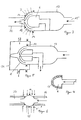
- domes 1 shows several domes 1, which are arranged next to one another in a grid on the base plate 2 of a recipient 3 for coating with a plasma pulse method.
- the domes 1 are sunk into corresponding depressions 4 in the base plate 2.
- the cover plate 5 of the recipient 3 is provided in accordance with the arrangement of the depressions 4 in the base plate 2 with an arrangement of displacement bodies 6 which are immersed in the cavities 8 delimited by the spherical cap surfaces 7 to be coated.
- Each displacement body 6 is provided for supplying the reaction gases with a central channel 9, which can be connected to a gas source, not shown in the figure.
- a plurality of gas outlet openings 10 are provided in the side walls of the recipient 3, through which the reaction gases depleted in layer material can be sucked off by means of a vacuum pump (not shown).
- the distance between a dome inner surface 7 and the side 11 of the associated displacement body 6 opposite this is dimensioned such that the particle formation taking place in the gas space between the two surfaces during a plasma discharge does not impair the layer quality.
- the means for generating the plasma zone in the recipient are known per se and are therefore not shown in the figure.
- the plasma can be excited capacitively in such a way that both the bottom and the top plate of the recipient consist of a metal and a voltage is applied between the two plates.
- both dielectric and metallic layers or mixed layers of dielectric and metallic materials can be deposited.
- the reaction gases are introduced through the displacement bodies 6 in a continuous gas flow into the cavities 8 delimited by the calotte inner surfaces 7 and the displacement bodies 6.
- the gas flow is deflected and guided along the surface to be coated laterally past the displacement body 6 and out of the cap 1 (the solid arrows in the figure indicate the gas flow direction).
- 3 layer material is deposited on the inner surface 7 of the spherical cap, the surface of the displacement body 6 and on the entire inner wall of the recipient.
- the time period between two plasma pulses and the gas mass flow are expediently coordinated with one another, as is customary in plasma pulse CVD processes, in such a way that the reaction space above the inner surface of the calotte is completely filled with fresh reaction gases before each plasma pulse.
- the device from FIG. 1 can be installed in an oven. It is easier to bring the substrates to the desired substrate temperature by means of a plasma pretreatment.
- Figures 2 and 3 show devices for coating individual domes. It can be seen that in each case a spherical cap 1 with a vessel 13 which is open on one side is joined to form a recipient 3. A sealing ring 14 located between the edges of the two vessel parts ensures a gas-tight connection.
- the device in FIG. 2 is suitable for coating a cap with a closed cap neck.
- the reaction gases are supplied through a gas inlet opening 15 in the vessel part 13 attached to the calotte.
- reaction gases are passed past the displacement body 6, along the surface to be coated to the spherical cap 12, deflected there and via the channel 16 in the displacement body 6 and the angled glass tube 17 which carries the displacement body 6 and which is connected to a vacuum pump (not shown). aspirated.
- a straight glass tube which is axially arranged in the vacuum vessel and which is melted into the vessel wall opposite the spherical cap can also be used to hold the displacement body.
- the gas supply can e.g. through gas inlet openings grouped around the melting point.
- the plasma is excited by irradiation with microwave energy.
- a waveguide 18 is placed on the spherical cap 1, the outer conductor 19 of which extends to the edge of the spherical cap and the inner conductor 20 ends immediately in front of the closed spherical cap neck 12.
- the plasma area can easily be limited to the reaction space 21 delimited by the calotte inner surface 7 and the end surface 11 of the displacement body 6.
- the plasma area extends in part up to channel 16 in the displacement body; the fact that only the reaction gases depleted of layer material are passed through this channel, a gradual clogging of the opening and the channel with layer material is largely avoided.
- Figure 3 shows a device for coating a cap with an open cap neck.
- the coating is carried out essentially analogously to the embodiment in FIG. 2.
- the consumed reaction gases are not discharged through the displacement body 6, but through the open cap neck 12.
- a glass tube 22, which is connected to a vacuum pump, is placed on the calotte 1 from the outside and by means of a Sealing ring 14 securely sealed against the outside.
- the plasma can be excited, for example, by irradiating microwave energy (see dashed arrows) by means of microwave antennas, not shown, which are grouped laterally around the calotte.
- the displacement body 6 in FIG. 2 does not necessarily have to have a central channel 16, but, as shown in FIG. 4, can be provided with small channels 23 ( ⁇ ⁇ 1 mm) distributed uniformly over the entire surface (e.g. frit).
- a second vacuum vessel 24 above the cap which is equipped with a gas that does not attack the cap material or in a plasma itself on the cap Coating takes part (for example O2), is applied. If the size of the leak remains unchanged, the amount of gas flowing into the cap 1 will be smaller, the smaller the pressure difference between the inside and outside of the cap.
- the pressure in the vacuum vessel 24 is set so high that no plasma is just ignited there during the plasma coating of the inner surface 7 of the cap (p ⁇ 50 to 100 mbar).
- the measure described above can be important if many domes are coated at the same time from the same gas supply system. Without this measure, the coating of all domes can be endangered by a single leak.
- FIG. 6 Two small, hemispherical domes 1 which are joined to form a vacuum vessel 25. Due to the spherical shape of the vacuum vessel 25, the same amount of gas is located above each surface element of the substrate surface. A uniform coating is therefore guaranteed even without a displacement body when using a plasma pulse CVD process. The volume limited by the two domes is small enough to rule out any impairment of the layer quality due to a homogeneous reaction in the gas space.
- the gas flow takes place through the open spherical necks 12, to which gas supply and discharge pipes 26, 27 are attached in a gas-tight manner, analogous to the device in FIG.
- the plasma can also be excited in a simple manner by irradiation of microwave energy by means of microwave antennas grouped laterally around the vacuum vessel.
- the coating and displacement bodies are in principle interchangeable.
- the cap to be coated can be brought into the place of the displacement body. It is only necessary to ensure that there is no layer material in the interior of the calotte in order to avoid an inner coating occurring simultaneously with the outer coating.
- the spherical cap can, for example, be part of a further vacuum vessel arranged in the recipient.
- the device shown in FIG. 2 is particularly suitable for the coating of domes in mass production, since the vacuum vessel has only a single seal. It is advisable to install several of the vessels attached to the spheres firmly next to one another, arranged in a grid. The gas supply as well as the connection to a vacuum pump can take place via common supply systems.
- the spherical caps are placed on the permanently installed vessel halves, a sealing ring is used if necessary, and the vacuum vessels formed in this way are evacuated.
- the plasma can be excited in a simple manner by irradiating microwave energy, for example by means of waveguides placed on the calottes from above.
- the vacuum vessels are ventilated, whereupon the coated domes can simply be lifted off and replaced with new substrates.
- An Viton O-ring on the polished tube end ensures a vacuum-tight connection between the tube and the calotte.
- the tube is made of a dielectric material, in this case borosilicate glass No. 8330 from Schott Glastechnike.
- the reaction gases can be led into the reaction space thus formed through a laterally melted glass tube with a 10 mm diameter.
- the used reaction gases are removed by a taper at the end of the pipe. Dimensions can be taken from Figure 2, which is carried out on a scale of 1: 1.
- the gas supply pipe is angled on the axis of the larger pipe; it is completed with an axially pierced teflon displacement body.
- the diameter of the hole is 5 mm, but this value is not very critical.
- the reaction gases can enter the reaction space through this bore.
- the displacement body is shaped so that the distance from its surface to the inner surface of the Ka-lotte is the same everywhere except for the area under the spherical cap, namely 7 mm.
- an O2 gas discharge is ignited in the reaction space formed by the spherical cap and displacement body in order to condition the inner surface of the spherical cap to be coated.
- the desired substrate temperature is set via the intensity and duration of this O2 gas discharge.
- the microwave energy is radiated from above onto the calotte by a microwave antenna.
- the microwave radiation is interrupted and the gas mixture for producing the first TiO2 layer is set.
- This gas mixture is first allowed to flow into the bypass line for about 0.5 min; then the mass flows are stationary. During this time, the calotte cools only slightly.
- the TiO2 layer is produced using the parameters:
- the microwave radiation is interrupted and the gas mixture for producing the first SiO2 layer is set; with a steady mass flow (see above), the SiO2 layer is produced.
- a dome made of borosilicate glass No. 8486 from Schott Glaswerke with a diameter of 50 mm lies in a recipient on the lower electrode of a 13.56 MHz plasma generator.
- the upper electrode is designed as a gas shower and displacement body. The distance between the displacement body and the inner surface of the substrate to be coated is 15 mm at each point on the substrate.
- the recipient is evacuated to 0.03 mbar and the dome is pretreated with an O2 gas discharge at this pressure. Then it is coated at the same pressure; a mass flow of 1 ml / 1 min TiCl4 and 35 ml O2 is set and a TiO2 layer is applied at an RF power of 50 W. Then a mass flow of 0.5 ml / min C6H18OSi2 (hexamethyldisiloxane) and 35 ml O2 is set and an SiO2 layer is applied at an RF power of 50 W.
- the layer thicknesses are adjusted according to known optical criteria so that the interference layer system is a cold light mirror.
Landscapes
- Chemical & Material Sciences (AREA)
- General Chemical & Material Sciences (AREA)
- Chemical Kinetics & Catalysis (AREA)
- Engineering & Computer Science (AREA)
- Materials Engineering (AREA)
- Organic Chemistry (AREA)
- Metallurgy (AREA)
- Mechanical Engineering (AREA)
- Life Sciences & Earth Sciences (AREA)
- Geochemistry & Mineralogy (AREA)
- Chemical Vapour Deposition (AREA)
- Optical Elements Other Than Lenses (AREA)
- Surface Treatment Of Optical Elements (AREA)
Applications Claiming Priority (2)
| Application Number | Priority Date | Filing Date | Title |
|---|---|---|---|
| DE4008405 | 1990-03-16 | ||
| DE4008405A DE4008405C1 (fr) | 1990-03-16 | 1990-03-16 |
Publications (3)
| Publication Number | Publication Date |
|---|---|
| EP0446596A2 true EP0446596A2 (fr) | 1991-09-18 |
| EP0446596A3 EP0446596A3 (en) | 1991-11-06 |
| EP0446596B1 EP0446596B1 (fr) | 1994-11-09 |
Family
ID=6402337
Family Applications (1)
| Application Number | Title | Priority Date | Filing Date |
|---|---|---|---|
| EP91101392A Expired - Lifetime EP0446596B1 (fr) | 1990-03-16 | 1991-02-02 | Procédé PCVD pour la production de substrats sous la forme de calotte pourvus à l'intérieur et/ou à l'extérieur de revêtements diélectriques et/ou métalliques |
Country Status (6)
| Country | Link |
|---|---|
| US (1) | US5154943A (fr) |
| EP (1) | EP0446596B1 (fr) |
| JP (1) | JP2628414B2 (fr) |
| CN (1) | CN1037703C (fr) |
| CA (1) | CA2038292C (fr) |
| DE (2) | DE4008405C1 (fr) |
Cited By (3)
| Publication number | Priority date | Publication date | Assignee | Title |
|---|---|---|---|---|
| EP0540082A1 (fr) * | 1991-10-28 | 1993-05-05 | International Business Machines Corporation | Réacteur de dépôt en phase vapeur sous basse pression pour une déposition de grande efficacité et uniformité et méthode par une telle déposition |
| EP0551737B1 (fr) * | 1991-12-13 | 1996-05-15 | AT&T Corp. | Procédé de dépÔt en phase vapeur pour le revêtement d'articles manufacturés |
| EP0811367A3 (fr) * | 1996-06-05 | 1997-12-17 | Schott Glaswerke | Récipient en verre particulièrement pour stocker des solutions pharmaceutiques ou diagnostiques |
Families Citing this family (60)
| Publication number | Priority date | Publication date | Assignee | Title |
|---|---|---|---|---|
| DE4120176C1 (fr) * | 1991-06-19 | 1992-02-27 | Schott Glaswerke, 6500 Mainz, De | |
| DE4228853C2 (de) | 1991-09-18 | 1993-10-21 | Schott Glaswerke | Optischer Wellenleiter mit einem planaren oder nur geringfügig gewölbten Substrat und Verfahren zu dessen Herstellung sowie Verwendung eines solchen |
| DE4137606C1 (fr) * | 1991-11-15 | 1992-07-30 | Schott Glaswerke, 6500 Mainz, De | |
| US5352487A (en) * | 1992-08-31 | 1994-10-04 | Gte Products Corporation | Process for the formation of SiO2 films |
| EP0595159B1 (fr) * | 1992-10-26 | 1997-12-29 | Schott Glaswerke | Procédé et appareillage pour revêtir par CVD l'intérieur des substrats fortement courbés sous la forme de calotte |
| DE4334572C2 (de) * | 1992-10-26 | 1995-12-07 | Schott Glaswerke | Verfahren und Vorrichtung zur Beschichtung der Innenfläche stark gewölbter im wesentlichen kalottenförmiger Substrate mittels CVD |
| JPH07333404A (ja) * | 1994-02-15 | 1995-12-22 | Dainippon Printing Co Ltd | 光学機能性膜、光学機能性フィルム、防眩性反射防止フィルム、その製造方法、偏光板および液晶表示装置 |
| EP0753082B1 (fr) * | 1994-03-29 | 1999-07-07 | Schott Glas | Procede plasma-cvd de revetement de substrats bombes |
| US5466906A (en) * | 1994-04-08 | 1995-11-14 | Ford Motor Company | Process for coating automotive engine cylinders |
| DE4438359C2 (de) | 1994-10-27 | 2001-10-04 | Schott Glas | Behälter aus Kunststoff mit einer Sperrbeschichtung |
| DE19540414C1 (de) * | 1995-10-30 | 1997-05-22 | Fraunhofer Ges Forschung | Kaltlichtreflektor |
| WO1997044503A1 (fr) * | 1996-05-22 | 1997-11-27 | Tetra Laval Holdings & Finance S.A. | Procede et appareil de traitement des surfaces interieures de recipients |
| DE19629877C1 (de) * | 1996-07-24 | 1997-03-27 | Schott Glaswerke | CVD-Verfahren und Vorrichtung zur Innenbeschichtung von Hohlkörpern |
| DE19634795C2 (de) * | 1996-08-29 | 1999-11-04 | Schott Glas | Plasma-CVD-Anlage mit einem Array von Mikrowellen-Plasmaelektroden und Plasma-CVD-Verfahren |
| DE19740806C2 (de) * | 1997-09-17 | 1999-10-07 | Schott Glas | Mikrotiterplatte aus Kunststoff |
| DE19754056C1 (de) * | 1997-12-05 | 1999-04-08 | Schott Glas | Verfahren zum Beschichten von Elastomerkomponenten |
| US20020011215A1 (en) * | 1997-12-12 | 2002-01-31 | Goushu Tei | Plasma treatment apparatus and method of manufacturing optical parts using the same |
| DE19801320B4 (de) * | 1998-01-16 | 2004-08-26 | Schott Glas | Befüllter und verschlossener Kunststoffbehälter und Verfahren zu seiner Herstellung |
| DE19801861C2 (de) | 1998-01-20 | 2001-10-18 | Schott Glas | Verfahren zum Herstellen eines hohlen, innenbeschichteten Glasformkörpers |
| AT3549U1 (de) * | 1998-05-04 | 2000-04-25 | Inocon Technologie Gmbh | Verfahren und einrichtung zum erzeugen von plasma |
| US6629763B2 (en) * | 2000-06-17 | 2003-10-07 | Schott Glas | Object which has optical layers |
| DE10029905A1 (de) * | 2000-06-17 | 2002-01-03 | Schott Auer Gmbh | Reflektor, insbesondere zur Anwendung bei einem Kraftfahrzeug |
| DE10112731A1 (de) * | 2001-03-14 | 2002-10-02 | Schott Glas | Beschichtung von Substraten |
| WO2002077319A1 (fr) * | 2001-03-27 | 2002-10-03 | Small & Medium Industry Promotion Corporation | Appareil de depot de fil de diamant utilisant des micro-ondes et du plasma |
| DE10204363A1 (de) * | 2002-02-02 | 2003-08-14 | Schott Glas | Interferenzbeschichtung zur Verbesserung des Energiehaushaltes von HID-Lampen |
| CN100374617C (zh) * | 2002-05-24 | 2008-03-12 | 肖特股份公司 | 化学气相沉积涂涂料设备 |
| DE10242752B4 (de) * | 2002-09-13 | 2005-01-13 | Schott Glas | Vorrichtung und Verfahren zum automatischen Beschicken einer Vielzahl von Bearbeitungsstationen sowie Beschichtungsanlage mit einer derartigen Vorrichtung |
| US6936547B2 (en) * | 2002-10-31 | 2005-08-30 | Micron Technology, Inc.. | Gas delivery system for deposition processes, and methods of using same |
| EP1625099A2 (fr) | 2003-04-01 | 2006-02-15 | Corning Incorporated | Substrat pour reflecteur de lampe, verre, materiaux vitro-ceramiques et procedes de fabrication |
| US7758936B2 (en) * | 2003-09-18 | 2010-07-20 | Boehringer Ingelheim Gmbh | Pharmaceutical blister |
| DE10343668A1 (de) * | 2003-09-18 | 2005-04-14 | Boehringer Ingelheim Pharma Gmbh & Co. Kg | Arzneimittelblister |
| DE102005040266A1 (de) * | 2005-08-24 | 2007-03-01 | Schott Ag | Verfahren und Vorrichtung zur innenseitigen Plasmabehandlung von Hohlkörpern |
| CN101441278A (zh) * | 2007-11-20 | 2009-05-27 | 鸿富锦精密工业(深圳)有限公司 | 固持装置及固持方法 |
| WO2013170052A1 (fr) | 2012-05-09 | 2013-11-14 | Sio2 Medical Products, Inc. | Enrobage protecteur en saccharide pour conditionnement pharmaceutique |
| MX350703B (es) | 2009-05-13 | 2017-09-14 | Sio2 Medical Products Inc | Metodo de gasificacion para inspeccionar una superficie revestida. |
| US7985188B2 (en) * | 2009-05-13 | 2011-07-26 | Cv Holdings Llc | Vessel, coating, inspection and processing apparatus |
| DE102009025971A1 (de) * | 2009-06-15 | 2010-12-16 | Aixtron Ag | Verfahren zum Einrichten eines Epitaxie-Reaktors |
| US9458536B2 (en) | 2009-07-02 | 2016-10-04 | Sio2 Medical Products, Inc. | PECVD coating methods for capped syringes, cartridges and other articles |
| US11624115B2 (en) | 2010-05-12 | 2023-04-11 | Sio2 Medical Products, Inc. | Syringe with PECVD lubrication |
| US9878101B2 (en) | 2010-11-12 | 2018-01-30 | Sio2 Medical Products, Inc. | Cyclic olefin polymer vessels and vessel coating methods |
| DE102010055659A1 (de) | 2010-12-22 | 2012-06-28 | Technische Universität Dresden | Verfahren zum Abscheiden dielektrischer Schichten im Vakuum sowie Verwendung des Verfahrens |
| US9272095B2 (en) | 2011-04-01 | 2016-03-01 | Sio2 Medical Products, Inc. | Vessels, contact surfaces, and coating and inspection apparatus and methods |
| US11116695B2 (en) | 2011-11-11 | 2021-09-14 | Sio2 Medical Products, Inc. | Blood sample collection tube |
| EP2776603B1 (fr) | 2011-11-11 | 2019-03-06 | SiO2 Medical Products, Inc. | Revêtement de passivation, de protection de ph ou à pouvoir lubrifiant pour conditionnement pharmaceutique, processus et appareil de revêtement |
| US20150297800A1 (en) | 2012-07-03 | 2015-10-22 | Sio2 Medical Products, Inc. | SiOx BARRIER FOR PHARMACEUTICAL PACKAGE AND COATING PROCESS |
| CA2890066C (fr) | 2012-11-01 | 2021-11-09 | Sio2 Medical Products, Inc. | Procedes d'inspection de revetement |
| US9903782B2 (en) | 2012-11-16 | 2018-02-27 | Sio2 Medical Products, Inc. | Method and apparatus for detecting rapid barrier coating integrity characteristics |
| JP6382830B2 (ja) | 2012-11-30 | 2018-08-29 | エスアイオーツー・メディカル・プロダクツ・インコーポレイテッド | 医療シリンジ、カートリッジ等上でのpecvd堆積の均一性制御 |
| US9764093B2 (en) | 2012-11-30 | 2017-09-19 | Sio2 Medical Products, Inc. | Controlling the uniformity of PECVD deposition |
| US9662450B2 (en) | 2013-03-01 | 2017-05-30 | Sio2 Medical Products, Inc. | Plasma or CVD pre-treatment for lubricated pharmaceutical package, coating process and apparatus |
| US9937099B2 (en) | 2013-03-11 | 2018-04-10 | Sio2 Medical Products, Inc. | Trilayer coated pharmaceutical packaging with low oxygen transmission rate |
| EP2971228B1 (fr) | 2013-03-11 | 2023-06-21 | Si02 Medical Products, Inc. | Emballage revêtu |
| US20160017490A1 (en) | 2013-03-15 | 2016-01-21 | Sio2 Medical Products, Inc. | Coating method |
| DE102013219213A1 (de) * | 2013-09-24 | 2015-03-26 | Osram Gmbh | Prozesskammer für einen chemischen Reaktionsbeschichtungsprozess und Verfahren zum Beschichten eines optischen Objekts mittels eines chemischen Reaktionsbeschichtungsprozesses |
| WO2015148471A1 (fr) | 2014-03-28 | 2015-10-01 | Sio2 Medical Products, Inc. | Revêtements antistatiques pour des récipients en plastique |
| EP3337915B1 (fr) | 2015-08-18 | 2021-11-03 | SiO2 Medical Products, Inc. | Conditionnement pharmaceutique et autre présentant un faible taux de transmission d'oxygène |
| JP6850636B2 (ja) * | 2017-03-03 | 2021-03-31 | 東京エレクトロン株式会社 | プラズマ処理装置 |
| EP3980574A1 (fr) | 2019-06-10 | 2022-04-13 | SweGaN AB | Réacteur pour le traitement au gaz d'un substrat |
| KR102203878B1 (ko) * | 2019-06-11 | 2021-01-15 | 한양대학교 산학협력단 | 기판 처리 장치 및 기판 처리 방법 |
| CN110339656B (zh) * | 2019-07-19 | 2020-08-25 | 北京双龙腾飞臭氧设备有限公司 | 一种ddbd双介质低温等离子环保设备 |
Family Cites Families (12)
| Publication number | Priority date | Publication date | Assignee | Title |
|---|---|---|---|---|
| US3731650A (en) * | 1971-11-03 | 1973-05-08 | Gen Electric | Gas distributor for casting mold manufacture |
| BE792316A (fr) * | 1971-12-07 | 1973-06-05 | Philips Nv | Procede permettant de realiser des miroirs pour lumiere froide |
| DE2718518C3 (de) * | 1977-04-26 | 1984-04-19 | Siemens Ag, 1000 Berlin Und 8000 Muenchen | Verfahren zum Abscheiden einer Schicht auf der Innenseite von Hohlräumen eines Werkstückes |
| DE2913843A1 (de) * | 1979-04-06 | 1980-10-23 | Philips Patentverwaltung | Verfahren zur herstellung von mikrolinsen und kopplungselement mit einer nach diesem verfahren hergestellten mikrolinse |
| US4602847A (en) * | 1984-06-04 | 1986-07-29 | Hans Zapfe | Method of producing optical elements having interference layers |
| US4749589A (en) * | 1984-12-13 | 1988-06-07 | Stc Plc | Method of surface treatment |
| JPS63307192A (ja) * | 1987-06-06 | 1988-12-14 | Sumitomo Electric Ind Ltd | 化合物結晶の製造方法及びその装置 |
| JPS6452695A (en) * | 1987-08-25 | 1989-02-28 | Sumitomo Electric Industries | Synthesis of crystal by vapor growth |
| JPH01100277A (ja) * | 1987-10-12 | 1989-04-18 | Idemitsu Petrochem Co Ltd | 硬質炭素膜付着湾曲板、硬質炭素膜付着湾曲板の製造方法および硬質炭素膜付着湾曲板の製造装置 |
| DE3739528A1 (de) * | 1987-11-21 | 1989-06-01 | Bbc Brown Boveri & Cie | Cvd-rohrofenreaktor |
| DE3742204C2 (de) * | 1987-12-12 | 1995-10-26 | Leybold Ag | Verfahren zur Herstellung einer korrosionsfesten, weitgehend absorptionsfreien Schicht auf der Oberfläche eines Werkstücks |
| DE3926023A1 (de) * | 1988-09-06 | 1990-03-15 | Schott Glaswerke | Cvd-beschichtungsverfahren zur herstellung von schichten und vorrichtung zur durchfuehrung des verfahrens |
-
1990
- 1990-03-16 DE DE4008405A patent/DE4008405C1/de not_active Expired - Lifetime
-
1991
- 1991-02-02 DE DE59103456T patent/DE59103456D1/de not_active Expired - Fee Related
- 1991-02-02 EP EP91101392A patent/EP0446596B1/fr not_active Expired - Lifetime
- 1991-03-14 CA CA002038292A patent/CA2038292C/fr not_active Expired - Fee Related
- 1991-03-15 JP JP3074275A patent/JP2628414B2/ja not_active Expired - Fee Related
- 1991-03-16 CN CN91101602A patent/CN1037703C/zh not_active Expired - Fee Related
- 1991-03-18 US US07/670,420 patent/US5154943A/en not_active Expired - Lifetime
Cited By (4)
| Publication number | Priority date | Publication date | Assignee | Title |
|---|---|---|---|---|
| EP0540082A1 (fr) * | 1991-10-28 | 1993-05-05 | International Business Machines Corporation | Réacteur de dépôt en phase vapeur sous basse pression pour une déposition de grande efficacité et uniformité et méthode par une telle déposition |
| EP0551737B1 (fr) * | 1991-12-13 | 1996-05-15 | AT&T Corp. | Procédé de dépÔt en phase vapeur pour le revêtement d'articles manufacturés |
| EP0811367A3 (fr) * | 1996-06-05 | 1997-12-17 | Schott Glaswerke | Récipient en verre particulièrement pour stocker des solutions pharmaceutiques ou diagnostiques |
| US6537626B1 (en) | 1996-06-05 | 2003-03-25 | Schott Glaswerke | CVD-coated glass container |
Also Published As
| Publication number | Publication date |
|---|---|
| DE4008405C1 (fr) | 1991-07-11 |
| JPH04224681A (ja) | 1992-08-13 |
| CN1055015A (zh) | 1991-10-02 |
| EP0446596A3 (en) | 1991-11-06 |
| CN1037703C (zh) | 1998-03-11 |
| JP2628414B2 (ja) | 1997-07-09 |
| CA2038292C (fr) | 1995-04-18 |
| US5154943A (en) | 1992-10-13 |
| EP0446596B1 (fr) | 1994-11-09 |
| DE59103456D1 (de) | 1994-12-15 |
Similar Documents
| Publication | Publication Date | Title |
|---|---|---|
| EP0446596B1 (fr) | Procédé PCVD pour la production de substrats sous la forme de calotte pourvus à l'intérieur et/ou à l'extérieur de revêtements diélectriques et/ou métalliques | |
| EP0753082B1 (fr) | Procede plasma-cvd de revetement de substrats bombes | |
| DE69019455T2 (de) | Reflektoren für Lampen. | |
| EP0529268B1 (fr) | Couche dure antireflet pour lentille en plastique | |
| DE10202311B4 (de) | Vorrichtung und Verfahren zur Plasmabehandlung von dielektrischen Körpern | |
| DE3830249A1 (de) | Plasmaverfahren zum beschichten ebener substrate | |
| DE2251571A1 (de) | Verfahren und vorrichtung zum aufbringen von beschichtungen auf substraten | |
| DE19912737A1 (de) | Verfahren zur Herstellung von porösen SiO¶x¶-Schichten und poröse SiO¶x¶-Schichten | |
| DE60314634T2 (de) | Titandioxid-beschichtungen hergestellt durch plasma-cvd bei atmosphärendruck | |
| EP0221968A1 (fr) | Procede pour enlever des ions metalliques d'articles en verre ou en materiaux ceramiques | |
| DE19824364A1 (de) | Verfahren zum Aufbringen eines Verschleißschutz-Schichtsystems mit optischen Eigenschaften auf Oberflächen | |
| DE102013208310A1 (de) | Optisches Element mit einer Beschichtung hoher Diffusivität | |
| DE10100746A1 (de) | Vorrichtung und Verfahren zum Bilden von Filmen | |
| US5236511A (en) | Plasma CVD process for coating a dome-shaped substrate | |
| EP0595159B1 (fr) | Procédé et appareillage pour revêtir par CVD l'intérieur des substrats fortement courbés sous la forme de calotte | |
| DE19652454C2 (de) | Verfahren und Vorrichtung zur Außenbeschichtung von Lampen | |
| EP1472195B1 (fr) | Procede pour appliquer un revetement sur un bruleur a quartz d'une lampe a decharge a haute intensite | |
| DE4414083C2 (de) | Vorrichtung zum Herstellen dünner Schichten auf Kunststoff-Substraten und zum Ätzen solcher Substrate | |
| EP1264004B1 (fr) | Procede et dispositif pour recouvrir des substrats | |
| DE3442208A1 (de) | Verfahren und vorrichtung zum herstellen harten kohlenstoffschichten | |
| DE4334572C2 (de) | Verfahren und Vorrichtung zur Beschichtung der Innenfläche stark gewölbter im wesentlichen kalottenförmiger Substrate mittels CVD | |
| DE4338040C2 (de) | Vorrichtung zum Beschichten von Brillengläsern im Vakuum und Betriebsverfahren hierfür | |
| DE69505837T2 (de) | Beschichtungen mit niedriger oberflächenenergie | |
| DE19634334C1 (de) | Wisch- und kratzfeste Reflexionsbeschichtung und Verfahren zu ihrer Herstellung | |
| EP0714455A1 (fr) | Procede permettant d'appliquer des couches de carbone diamantees sur un substrat |
Legal Events
| Date | Code | Title | Description |
|---|---|---|---|
| PUAI | Public reference made under article 153(3) epc to a published international application that has entered the european phase |
Free format text: ORIGINAL CODE: 0009012 |
|
| PUAL | Search report despatched |
Free format text: ORIGINAL CODE: 0009013 |
|
| AK | Designated contracting states |
Kind code of ref document: A2 Designated state(s): BE CH DE FR GB IT LI NL |
|
| AK | Designated contracting states |
Kind code of ref document: A3 Designated state(s): BE CH DE FR GB IT LI NL |
|
| 17P | Request for examination filed |
Effective date: 19911126 |
|
| 17Q | First examination report despatched |
Effective date: 19931027 |
|
| GRAA | (expected) grant |
Free format text: ORIGINAL CODE: 0009210 |
|
| AK | Designated contracting states |
Kind code of ref document: B1 Designated state(s): BE CH DE FR GB IT LI NL |
|
| ET | Fr: translation filed | ||
| GBT | Gb: translation of ep patent filed (gb section 77(6)(a)/1977) |
Effective date: 19941107 |
|
| REF | Corresponds to: |
Ref document number: 59103456 Country of ref document: DE Date of ref document: 19941215 |
|
| ITF | It: translation for a ep patent filed | ||
| PLBE | No opposition filed within time limit |
Free format text: ORIGINAL CODE: 0009261 |
|
| STAA | Information on the status of an ep patent application or granted ep patent |
Free format text: STATUS: NO OPPOSITION FILED WITHIN TIME LIMIT |
|
| 26N | No opposition filed | ||
| REG | Reference to a national code |
Ref country code: GB Ref legal event code: IF02 |
|
| PGFP | Annual fee paid to national office [announced via postgrant information from national office to epo] |
Ref country code: CH Payment date: 20040203 Year of fee payment: 14 |
|
| PGFP | Annual fee paid to national office [announced via postgrant information from national office to epo] |
Ref country code: NL Payment date: 20040204 Year of fee payment: 14 |
|
| PGFP | Annual fee paid to national office [announced via postgrant information from national office to epo] |
Ref country code: BE Payment date: 20040401 Year of fee payment: 14 |
|
| PGFP | Annual fee paid to national office [announced via postgrant information from national office to epo] |
Ref country code: GB Payment date: 20050131 Year of fee payment: 15 |
|
| PG25 | Lapsed in a contracting state [announced via postgrant information from national office to epo] |
Ref country code: IT Free format text: LAPSE BECAUSE OF NON-PAYMENT OF DUE FEES;WARNING: LAPSES OF ITALIAN PATENTS WITH EFFECTIVE DATE BEFORE 2007 MAY HAVE OCCURRED AT ANY TIME BEFORE 2007. THE CORRECT EFFECTIVE DATE MAY BE DIFFERENT FROM THE ONE RECORDED. Effective date: 20050202 |
|
| PGFP | Annual fee paid to national office [announced via postgrant information from national office to epo] |
Ref country code: DE Payment date: 20050208 Year of fee payment: 15 |
|
| PGFP | Annual fee paid to national office [announced via postgrant information from national office to epo] |
Ref country code: FR Payment date: 20050210 Year of fee payment: 15 |
|
| PG25 | Lapsed in a contracting state [announced via postgrant information from national office to epo] |
Ref country code: LI Free format text: LAPSE BECAUSE OF NON-PAYMENT OF DUE FEES Effective date: 20050228 Ref country code: CH Free format text: LAPSE BECAUSE OF NON-PAYMENT OF DUE FEES Effective date: 20050228 Ref country code: BE Free format text: LAPSE BECAUSE OF NON-PAYMENT OF DUE FEES Effective date: 20050228 |
|
| BERE | Be: lapsed |
Owner name: *SCHOTT GLASWERKE Effective date: 20050228 |
|
| PG25 | Lapsed in a contracting state [announced via postgrant information from national office to epo] |
Ref country code: NL Free format text: LAPSE BECAUSE OF NON-PAYMENT OF DUE FEES Effective date: 20050901 |
|
| REG | Reference to a national code |
Ref country code: CH Ref legal event code: PL |
|
| NLV4 | Nl: lapsed or anulled due to non-payment of the annual fee |
Effective date: 20050901 |
|
| PG25 | Lapsed in a contracting state [announced via postgrant information from national office to epo] |
Ref country code: GB Free format text: LAPSE BECAUSE OF NON-PAYMENT OF DUE FEES Effective date: 20060202 |
|
| PG25 | Lapsed in a contracting state [announced via postgrant information from national office to epo] |
Ref country code: DE Free format text: LAPSE BECAUSE OF NON-PAYMENT OF DUE FEES Effective date: 20060901 |
|
| GBPC | Gb: european patent ceased through non-payment of renewal fee |
Effective date: 20060202 |
|
| REG | Reference to a national code |
Ref country code: FR Ref legal event code: ST Effective date: 20061031 |
|
| BERE | Be: lapsed |
Owner name: *SCHOTT GLASWERKE Effective date: 20050228 |
|
| PG25 | Lapsed in a contracting state [announced via postgrant information from national office to epo] |
Ref country code: FR Free format text: LAPSE BECAUSE OF NON-PAYMENT OF DUE FEES Effective date: 20060228 |