EP0446639A2 - Convertisseur analogique numÀ©rique parallèle - Google Patents
Convertisseur analogique numÀ©rique parallèle Download PDFInfo
- Publication number
- EP0446639A2 EP0446639A2 EP91102121A EP91102121A EP0446639A2 EP 0446639 A2 EP0446639 A2 EP 0446639A2 EP 91102121 A EP91102121 A EP 91102121A EP 91102121 A EP91102121 A EP 91102121A EP 0446639 A2 EP0446639 A2 EP 0446639A2
- Authority
- EP
- European Patent Office
- Prior art keywords
- differential amplifier
- output
- input
- stages
- decision
- Prior art date
- Legal status (The legal status is an assumption and is not a legal conclusion. Google has not performed a legal analysis and makes no representation as to the accuracy of the status listed.)
- Granted
Links
Images

Classifications
-
- H—ELECTRICITY
- H03—ELECTRONIC CIRCUITRY
- H03M—CODING; DECODING; CODE CONVERSION IN GENERAL
- H03M1/00—Analogue/digital conversion; Digital/analogue conversion
- H03M1/12—Analogue/digital converters
- H03M1/20—Increasing resolution using an n bit system to obtain n + m bits
- H03M1/202—Increasing resolution using an n bit system to obtain n + m bits by interpolation
- H03M1/203—Increasing resolution using an n bit system to obtain n + m bits by interpolation using an analogue interpolation circuit
- H03M1/204—Increasing resolution using an n bit system to obtain n + m bits by interpolation using an analogue interpolation circuit in which one or more virtual intermediate reference signals are generated between adjacent original reference signals, e.g. by connecting pre-amplifier outputs to multiple comparators
-
- H—ELECTRICITY
- H03—ELECTRONIC CIRCUITRY
- H03M—CODING; DECODING; CODE CONVERSION IN GENERAL
- H03M1/00—Analogue/digital conversion; Digital/analogue conversion
- H03M1/12—Analogue/digital converters
- H03M1/34—Analogue value compared with reference values
- H03M1/36—Analogue value compared with reference values simultaneously only, i.e. parallel type
- H03M1/361—Analogue value compared with reference values simultaneously only, i.e. parallel type having a separate comparator and reference value for each quantisation level, i.e. full flash converter type
- H03M1/362—Analogue value compared with reference values simultaneously only, i.e. parallel type having a separate comparator and reference value for each quantisation level, i.e. full flash converter type the reference values being generated by a resistive voltage divider
- H03M1/365—Analogue value compared with reference values simultaneously only, i.e. parallel type having a separate comparator and reference value for each quantisation level, i.e. full flash converter type the reference values being generated by a resistive voltage divider the voltage divider being a single resistor string
Definitions
- the invention relates to an analog / digital converter according to the preamble of claim 1.
- Figure 1 shows an input stage with differential amplifier stages and decision stages of such an analog / digital converter according to the prior art
- FIG. 1 shows an input stage of an analog / digital converter with a plurality of differential amplifier stages, each formed from a first transistor Ta and a second transistor Tb, the emitter connections of which are each connected to a constant current source Ie, which is connected to reference potential.
- the collector terminal of the first transistor Ta forms a first output of a differential amplifier stage and is connected to supply potential Vcc via a resistor Ra.
- the collector connection of the second transistor Tb forms the second output of this differential amplifier stage and is connected in the example to the supply potential V CC via a resistor Rb and the two outputs of the differential amplifier stages are each connected to the two inputs of a decision stage En, En + 1 ... .
- the base connection of the second transistor Tb of these differential amplifier stages is acted upon in each case by the analog signal Uan, the base connection of the first transistor Ta of these differential amplifier stages is in each case at a fixed potential ... U n-4 , U n-3 , U n-2 , .. .switched, this fixed potential differing between two successive differential amplifier stages by a fixed value.
- This is achieved in that an equally large resistor R is connected between the base connections of the respective first transistor of successive differential amplifier stages in such a way that all of these Resistors R form a series circuit and a constant current Ir flows through them.
- the primarily capacitive input conductance of a differential amplifier circuit leads to a change in the analog signal.
- the dynamic behavior of an analog / digital converter is negatively affected by the distortions of the analog signal due to the non-linear input capacitance.
- the object of the invention is to provide an analog / digital converter which, with the same resolution, requires a smaller number of differential amplifier stages and a smaller number of resistors in the reference voltage generation associated with these differential amplifier stages.
- Figure 2 shows the input stage of an analog / digital converter with a plurality of differential amplifier stages Ta, Tb, Ra, Rb, Ie, each with a first and a second input and a first and a second output A1, A2.
- the differential input voltage two successive differential amplifier stages each differ by a fixed value, since the base connection of the first transistor Ta is connected via a resistor R to the base connection of the first transistor Ta of the two adjacent differential amplifier stages Ta, Tb, Ra, Rb, Ie.
- the differential amplifier stages Ta, Tb, ... each have a first and a second output A1, A2.
- the first output A1 of each differential amplifier stage Ta, Tb, ... is connected to the first input of a decision stage, e.g. En, switched and also it is at the first input of one of the two decision stages En-1; En + 1 switched, whose switching threshold differs the least from the switching threshold of this decision level En.
- circuits according to FIG. 2 only require 2 k ⁇ 1 differential amplifier stages and also resistors R in the reference voltage generation circuit to implement an analog / digital converter with a resolution of k bits. Since the resistors R in the reference voltage generation circuit are very difficult to implement, such a circuit brings economic advantages. In addition, the dynamic behavior of such an analog / digital converter is improved over that of the prior art in that half as many differential amplifiers load the analog signal Uan, so that the nonlinear distortions of the analog signal are not as great.
- the decision stages switched between two different differential amplifier stages ..., En-3, En-1, En + 1, ... are switched in such a way that their switching threshold lies exactly between the switching thresholds of the two decision stages, the inputs of each of which are at the two outputs the differential amplifier circuits are connected, at the outputs of which the intermediate decision stage is connected.
- the decision stage En + 1 switches, for example, if the following applies to the analog signal Uan: U n and U n + 2 are potentials at two circuit nodes that are separated by a resistor R.
- the switching threshold set by this formula corresponds to the switching threshold of the decision stage En + 1, the assigned differential amplifier having the reference potential U n + 1 applied to it.
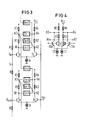
- FIG. 3 shows a circuit arrangement according to the invention in the event that each differential amplifier circuit Ta, Tb, ... has a first A1, a second A2, a third A3 and a fourth A4 output, the potential at the third output A3 of each differential amplifier always from Potential at the first output A1 differs, the potential at the fourth output A4 of each differential amplifier always being different from the potential at the second output A2 and the voltage between the first and second outputs A1, A2 and the voltage between the third and fourth outputs A3 , A4 - always have the same sign in every operating case.
- the first with the second output A1, A2 and the third with the fourth output A3, A4 are each provided for providing a symmetrical output signal of this differential amplifier.
- such a differential amplifier shown in FIG. 3 it consists of a first transistor Ta and a second transistor Tb, whose emitter connections are connected to a current source Ie, which is connected to reference potential.
- the collector terminal of the first transistor Ta forms a first output A1 of the circuit and is connected to the supply potential V CC via the series circuit of two resistors R1 and R3.
- the connection node between the resistor R1 and the resistor R3 forms the third output A3.
- the collector of the second transistor Tb forms the second output A2 and is connected to the supply potential V CC via the series connection of two resistors R2 and R4.
- the connection node of resistor R2 and resistor R4 forms the fourth output A4 of the differential amplifier circuit.
- the base connections of the transistors Ta and Tb form the two input terminals of this circuit.
- each differential amplifier circuit Ta, Tb, ... is assigned a decision stage ..., En-4, En, ..., the two inputs of which each provide a symmetrical output signal from this differential amplifier circuit Ta, Tb, ...
- outputs A3, A4 are connected. It would also be possible to use outputs A1 and A2 for this.
- the first of these outputs, here the third A3, alternatively the first output A1 is connected to the first input of a decision stage ..., En-2, En + 2, ..., the second input of which is connected to the output corresponding to the second of these outputs , here with the fourth output A4, alternatively with the second output A2 which is connected to the differential amplifier circuit which is driven by the smallest differential voltage.
- FIG. 4 shows a further possible differential amplifier stage for use in a circuit arrangement according to FIG. 3.
- the first circuit input of this differential amplifier stage is formed by the base connections of a transistor T1a and a transistor T2a.
- the second circuit input of this differential amplifier stage is formed by the base connections of two transistors T1b and T2b.
- the emitter connection of the transistor T1a is connected to the reference potential together with the emitter connection of the transistor T1b via a constant current source I2.
- the emitter connection of the transistor T2a is connected to the reference potential together with the emitter connection of the transistor T2b via a further current source I1.
- the collector terminal of the transistor T2a forms the first output A1 of the differential amplifier stage and is connected to the supply potential V CC via the series connection of two resistors R1 and R3.
- the connection node between the resistors R1 and R3 forms the third output of the differential amplifier stage and is connected to the collector terminal of the transistor T1a.
- the collector terminal of transistor T2b forms the second output A2 of the differential amplifier stage and is connected to the supply potential V CC via the series connection of two resistors R2 and R4.
- the connection node of the resistors R2 and R4 forms the fourth output A4 of the differential amplifier stage and is connected to the collector terminal of the transistor T1b.
- the equation changes to: Another advantage of circuits with two resistors in the collector circuit of the differential amplifier stages is that the amplifier can have any non-linear behavior due to the low resolution. The temperature dependency can be eliminated by an appropriate resistance ratio. In addition, the circuit is completely independent of the selected current Ie
Landscapes
- Engineering & Computer Science (AREA)
- Theoretical Computer Science (AREA)
- Analogue/Digital Conversion (AREA)
- Amplifiers (AREA)
Applications Claiming Priority (2)
| Application Number | Priority Date | Filing Date | Title |
|---|---|---|---|
| DE4004748 | 1990-02-15 | ||
| DE4004748 | 1990-02-15 |
Publications (3)
| Publication Number | Publication Date |
|---|---|
| EP0446639A2 true EP0446639A2 (fr) | 1991-09-18 |
| EP0446639A3 EP0446639A3 (en) | 1993-06-16 |
| EP0446639B1 EP0446639B1 (fr) | 1996-11-13 |
Family
ID=6400247
Family Applications (1)
| Application Number | Title | Priority Date | Filing Date |
|---|---|---|---|
| EP91102121A Expired - Lifetime EP0446639B1 (fr) | 1990-02-15 | 1991-02-14 | Convertisseur analogique numérique parallèle |
Country Status (3)
| Country | Link |
|---|---|
| EP (1) | EP0446639B1 (fr) |
| AT (1) | ATE145306T1 (fr) |
| DE (1) | DE59108338D1 (fr) |
Cited By (1)
| Publication number | Priority date | Publication date | Assignee | Title |
|---|---|---|---|---|
| RU2157048C2 (ru) * | 1995-01-30 | 2000-09-27 | Самсунг Электроникс Ко., Лтд. | Аналого-цифровой преобразователь |
Family Cites Families (1)
| Publication number | Priority date | Publication date | Assignee | Title |
|---|---|---|---|---|
| US4928103A (en) * | 1989-09-18 | 1990-05-22 | Analog Devices, Inc. | Parallel analog-to-digital converter using 2.sup.(n-1) comparators |
-
1991
- 1991-02-14 AT AT91102121T patent/ATE145306T1/de not_active IP Right Cessation
- 1991-02-14 DE DE59108338T patent/DE59108338D1/de not_active Expired - Fee Related
- 1991-02-14 EP EP91102121A patent/EP0446639B1/fr not_active Expired - Lifetime
Cited By (1)
| Publication number | Priority date | Publication date | Assignee | Title |
|---|---|---|---|---|
| RU2157048C2 (ru) * | 1995-01-30 | 2000-09-27 | Самсунг Электроникс Ко., Лтд. | Аналого-цифровой преобразователь |
Also Published As
| Publication number | Publication date |
|---|---|
| EP0446639B1 (fr) | 1996-11-13 |
| ATE145306T1 (de) | 1996-11-15 |
| DE59108338D1 (de) | 1996-12-19 |
| EP0446639A3 (en) | 1993-06-16 |
Similar Documents
| Publication | Publication Date | Title |
|---|---|---|
| DE60036776T2 (de) | Verstärkerschaltung | |
| DE19958049B4 (de) | Transkonduktor und Strommodus D/A-Wandler | |
| DE68926184T2 (de) | DA-Wandler | |
| DE102009058793B4 (de) | Digital-Analog-Konverter mit Schaltkreisarchitekturen, um Schalterverluste zu beseitigen | |
| EP0236525A1 (fr) | Ligne à retard intégrée pour signaux numériques utilisant des transistors à effet de champ | |
| DE2059933B2 (de) | Digital-Analog-Umsetzer | |
| DE69416661T2 (de) | Digital Analogwandler | |
| DE69609272T2 (de) | Verstärkerstufe mit schaltbarer verstärkung und reduzierten verzerrungen | |
| DE3339498A1 (de) | Schnelle logische schaltung | |
| EP0939494B1 (fr) | Montage de convertisseurs numériques-analogiques du type à courant | |
| EP0217223B1 (fr) | Convertisseur numérique-analogique à compensation de température | |
| EP0080174A2 (fr) | Convertisseur digital-analogique intégrable | |
| EP0515432A1 (fr) | Convertisseur analogique/numerique differentiel | |
| DE3528550C2 (fr) | ||
| DE3306310C2 (fr) | ||
| DE69404808T2 (de) | Treiberschaltungen | |
| DE2925008A1 (de) | Integrierte strom-treiberschaltung | |
| DE69306603T2 (de) | Stromteiler sowie integrierte Schaltung mit mehreren Stromteilern | |
| DE69615638T2 (de) | Spannungsverstärker mit grossen dynamischen Bereich und A/D-Konverter damit | |
| EP0446639B1 (fr) | Convertisseur analogique numérique parallèle | |
| DE2803099C3 (de) | Digital-Analog-Umsetzer in integrierter Schaltungstechnik | |
| DE3788611T2 (de) | Kodeumsetzer mit komplementären Ausgangsspannungen. | |
| DE69414538T2 (de) | Digital/Analogwandlerschaltung | |
| EP0610770B1 (fr) | Montage de multiplexage à commutation de courant | |
| EP0133618A1 (fr) | Circuit oscillateur haute fréquence à quartz sous forme de circuit intégré monolithique |
Legal Events
| Date | Code | Title | Description |
|---|---|---|---|
| PUAI | Public reference made under article 153(3) epc to a published international application that has entered the european phase |
Free format text: ORIGINAL CODE: 0009012 |
|
| AK | Designated contracting states |
Kind code of ref document: A2 Designated state(s): AT DE FR GB IT NL |
|
| PUAL | Search report despatched |
Free format text: ORIGINAL CODE: 0009013 |
|
| AK | Designated contracting states |
Kind code of ref document: A3 Designated state(s): AT DE FR GB IT NL |
|
| 17P | Request for examination filed |
Effective date: 19930804 |
|
| 17Q | First examination report despatched |
Effective date: 19950515 |
|
| GRAG | Despatch of communication of intention to grant |
Free format text: ORIGINAL CODE: EPIDOS AGRA |
|
| GRAH | Despatch of communication of intention to grant a patent |
Free format text: ORIGINAL CODE: EPIDOS IGRA |
|
| GRAH | Despatch of communication of intention to grant a patent |
Free format text: ORIGINAL CODE: EPIDOS IGRA |
|
| GRAA | (expected) grant |
Free format text: ORIGINAL CODE: 0009210 |
|
| AK | Designated contracting states |
Kind code of ref document: B1 Designated state(s): AT DE FR GB IT NL |
|
| REF | Corresponds to: |
Ref document number: 145306 Country of ref document: AT Date of ref document: 19961115 Kind code of ref document: T |
|
| REF | Corresponds to: |
Ref document number: 59108338 Country of ref document: DE Date of ref document: 19961219 |
|
| ET | Fr: translation filed | ||
| ITF | It: translation for a ep patent filed | ||
| GBT | Gb: translation of ep patent filed (gb section 77(6)(a)/1977) |
Effective date: 19970122 |
|
| PLBE | No opposition filed within time limit |
Free format text: ORIGINAL CODE: 0009261 |
|
| STAA | Information on the status of an ep patent application or granted ep patent |
Free format text: STATUS: NO OPPOSITION FILED WITHIN TIME LIMIT |
|
| 26N | No opposition filed | ||
| REG | Reference to a national code |
Ref country code: GB Ref legal event code: IF02 |
|
| PGFP | Annual fee paid to national office [announced via postgrant information from national office to epo] |
Ref country code: AT Payment date: 20020123 Year of fee payment: 12 |
|
| PGFP | Annual fee paid to national office [announced via postgrant information from national office to epo] |
Ref country code: NL Payment date: 20020218 Year of fee payment: 12 |
|
| PG25 | Lapsed in a contracting state [announced via postgrant information from national office to epo] |
Ref country code: AT Free format text: LAPSE BECAUSE OF NON-PAYMENT OF DUE FEES Effective date: 20030214 |
|
| PG25 | Lapsed in a contracting state [announced via postgrant information from national office to epo] |
Ref country code: NL Free format text: LAPSE BECAUSE OF NON-PAYMENT OF DUE FEES Effective date: 20030901 |
|
| NLV4 | Nl: lapsed or anulled due to non-payment of the annual fee |
Effective date: 20030901 |
|
| PG25 | Lapsed in a contracting state [announced via postgrant information from national office to epo] |
Ref country code: IT Free format text: LAPSE BECAUSE OF NON-PAYMENT OF DUE FEES;WARNING: LAPSES OF ITALIAN PATENTS WITH EFFECTIVE DATE BEFORE 2007 MAY HAVE OCCURRED AT ANY TIME BEFORE 2007. THE CORRECT EFFECTIVE DATE MAY BE DIFFERENT FROM THE ONE RECORDED. Effective date: 20050214 |
|
| PGFP | Annual fee paid to national office [announced via postgrant information from national office to epo] |
Ref country code: FR Payment date: 20060216 Year of fee payment: 16 |
|
| PGFP | Annual fee paid to national office [announced via postgrant information from national office to epo] |
Ref country code: GB Payment date: 20060221 Year of fee payment: 16 |
|
| PGFP | Annual fee paid to national office [announced via postgrant information from national office to epo] |
Ref country code: DE Payment date: 20060418 Year of fee payment: 16 |
|
| GBPC | Gb: european patent ceased through non-payment of renewal fee |
Effective date: 20070214 |
|
| REG | Reference to a national code |
Ref country code: FR Ref legal event code: ST Effective date: 20071030 |
|
| PG25 | Lapsed in a contracting state [announced via postgrant information from national office to epo] |
Ref country code: DE Free format text: LAPSE BECAUSE OF NON-PAYMENT OF DUE FEES Effective date: 20070901 |
|
| PG25 | Lapsed in a contracting state [announced via postgrant information from national office to epo] |
Ref country code: GB Free format text: LAPSE BECAUSE OF NON-PAYMENT OF DUE FEES Effective date: 20070214 Ref country code: FR Free format text: LAPSE BECAUSE OF NON-PAYMENT OF DUE FEES Effective date: 20070228 |