EP0446647A2 - Caméra couleur digitale avec réglage automatique de la mise au point, de l'exposition et de l'équilibre des blancs - Google Patents
Caméra couleur digitale avec réglage automatique de la mise au point, de l'exposition et de l'équilibre des blancs Download PDFInfo
- Publication number
- EP0446647A2 EP0446647A2 EP91102206A EP91102206A EP0446647A2 EP 0446647 A2 EP0446647 A2 EP 0446647A2 EP 91102206 A EP91102206 A EP 91102206A EP 91102206 A EP91102206 A EP 91102206A EP 0446647 A2 EP0446647 A2 EP 0446647A2
- Authority
- EP
- European Patent Office
- Prior art keywords
- exposure
- auto
- detector
- signal
- focus
- Prior art date
- Legal status (The legal status is an assumption and is not a legal conclusion. Google has not performed a legal analysis and makes no representation as to the accuracy of the status listed.)
- Granted
Links
Images



Classifications
-
- H—ELECTRICITY
- H04—ELECTRIC COMMUNICATION TECHNIQUE
- H04N—PICTORIAL COMMUNICATION, e.g. TELEVISION
- H04N23/00—Cameras or camera modules comprising electronic image sensors; Control thereof
- H04N23/70—Circuitry for compensating brightness variation in the scene
- H04N23/75—Circuitry for compensating brightness variation in the scene by influencing optical camera components
-
- H—ELECTRICITY
- H04—ELECTRIC COMMUNICATION TECHNIQUE
- H04N—PICTORIAL COMMUNICATION, e.g. TELEVISION
- H04N23/00—Cameras or camera modules comprising electronic image sensors; Control thereof
- H04N23/60—Control of cameras or camera modules
- H04N23/67—Focus control based on electronic image sensor signals
- H04N23/673—Focus control based on electronic image sensor signals based on contrast or high frequency components of image signals, e.g. hill climbing method
-
- G—PHYSICS
- G03—PHOTOGRAPHY; CINEMATOGRAPHY; ANALOGOUS TECHNIQUES USING WAVES OTHER THAN OPTICAL WAVES; ELECTROGRAPHY; HOLOGRAPHY
- G03B—APPARATUS OR ARRANGEMENTS FOR TAKING PHOTOGRAPHS OR FOR PROJECTING OR VIEWING THEM; APPARATUS OR ARRANGEMENTS EMPLOYING ANALOGOUS TECHNIQUES USING WAVES OTHER THAN OPTICAL WAVES; ACCESSORIES THEREFOR
- G03B13/00—Viewfinders; Focusing aids for cameras; Means for focusing for cameras; Autofocus systems for cameras
- G03B13/32—Means for focusing
- G03B13/34—Power focusing
- G03B13/36—Autofocus systems
-
- G—PHYSICS
- G03—PHOTOGRAPHY; CINEMATOGRAPHY; ANALOGOUS TECHNIQUES USING WAVES OTHER THAN OPTICAL WAVES; ELECTROGRAPHY; HOLOGRAPHY
- G03B—APPARATUS OR ARRANGEMENTS FOR TAKING PHOTOGRAPHS OR FOR PROJECTING OR VIEWING THEM; APPARATUS OR ARRANGEMENTS EMPLOYING ANALOGOUS TECHNIQUES USING WAVES OTHER THAN OPTICAL WAVES; ACCESSORIES THEREFOR
- G03B3/00—Focusing arrangements of general interest for cameras, projectors or printers
- G03B3/10—Power-operated focusing
-
- H—ELECTRICITY
- H04—ELECTRIC COMMUNICATION TECHNIQUE
- H04N—PICTORIAL COMMUNICATION, e.g. TELEVISION
- H04N23/00—Cameras or camera modules comprising electronic image sensors; Control thereof
- H04N23/60—Control of cameras or camera modules
- H04N23/67—Focus control based on electronic image sensor signals
-
- H—ELECTRICITY
- H04—ELECTRIC COMMUNICATION TECHNIQUE
- H04N—PICTORIAL COMMUNICATION, e.g. TELEVISION
- H04N23/00—Cameras or camera modules comprising electronic image sensors; Control thereof
- H04N23/70—Circuitry for compensating brightness variation in the scene
- H04N23/71—Circuitry for evaluating the brightness variation
-
- H—ELECTRICITY
- H04—ELECTRIC COMMUNICATION TECHNIQUE
- H04N—PICTORIAL COMMUNICATION, e.g. TELEVISION
- H04N23/00—Cameras or camera modules comprising electronic image sensors; Control thereof
- H04N23/70—Circuitry for compensating brightness variation in the scene
- H04N23/72—Combination of two or more compensation controls
-
- H—ELECTRICITY
- H04—ELECTRIC COMMUNICATION TECHNIQUE
- H04N—PICTORIAL COMMUNICATION, e.g. TELEVISION
- H04N23/00—Cameras or camera modules comprising electronic image sensors; Control thereof
- H04N23/70—Circuitry for compensating brightness variation in the scene
- H04N23/73—Circuitry for compensating brightness variation in the scene by influencing the exposure time
-
- H—ELECTRICITY
- H04—ELECTRIC COMMUNICATION TECHNIQUE
- H04N—PICTORIAL COMMUNICATION, e.g. TELEVISION
- H04N23/00—Cameras or camera modules comprising electronic image sensors; Control thereof
- H04N23/80—Camera processing pipelines; Components thereof
- H04N23/84—Camera processing pipelines; Components thereof for processing colour signals
- H04N23/88—Camera processing pipelines; Components thereof for processing colour signals for colour balance, e.g. white-balance circuits or colour temperature control
Definitions
- This invention relates generally to a color video camera providing a digital video signal and having auto-focus, auto-exposure and auto-white balance functions, and further is directed to an exposure control system particularly suited for incorporation in such camera and which compensates for abnormal lighting conditions.
- the auto-exposure control system embodied in a conventional video camera controls the opening and closing of an iris and the gain of an auto gain control (AGC) circuit with the object of maintaining the luminance signal level in an exposure detection area of the CCD imaging device at a predetermined value.
- AGC auto gain control
- the conventional auto-exposure control system tends to open the iris and increase the gain of the AGC circuit with the result that objects in the foreground of the picture are saturated.
- Another object is to provide an auto-exposure control system for a video camera which is capable of accurately detecting the distribution of luminance signal levels for determination therefrom of the lighting condition so as to permit accurate control of the exposure, particularly in respect to objects in the foreground of the scene in the field of view of the camera.
- a video camera having a lens assembly for directing incident light onto a light reception surface of a pickup so as to form thereon an image corresponding to a scene in the field of view of the lens assembly so that the image pickup will provide a luminance signal corresponding to such light image, and exposure means for controlling the amount of the light incident on the surface; there are further provided: means for defining a plurality of exposure detection areas corresponding to respective portions of the light reception surface, first detector means for detecting levels of the luminance signal corresponding to the respective exposure detection areas, second detector means for detecting distributions of the levels of the luminance signal corresponding to the exposure detection areas, respectively, as an indication of the lighting condition to which the scene is subjected, control means for controlling the exposure means in response to the first detector means, and means for controlling positions and dimensions of the exposure detection areas relative to each other in response to the second detector means.
- outputs of the first detector means which represent levels of the luminance signal corresponding to the respective exposure detection areas are weighted relative to each other.
- the first detector means includes a peak detector and an integration detector for each of the exposure detection areas
- means are further provided for relatively weighting outputs of the peak detector and the integration detector for each of the exposure detection areas.
- the luminance signal is applied to the integration detector for each of the exposure detection areas through a non-linear transfer means having a characteristic which relatively reduces the effects of high amplitudes of the luminance signal on the outputs of the respective integration detectors.
- means are preferably provided for changing the characteristic of the non-linear transfer means in response to the distributions of the levels of the luminance signal corresponding to the respective exposure detection areas as determined by the second detector means.
- the plurality of exposure detection areas include first and second exposure detection areas which respectively correspond to central and peripheral portions of the light reception surface of the image pickup, or third and fourth exposure detection areas which respectively correspond to portions of such light reception surface extending thereacross one above the other, and the means for controlling positions and dimensions of the exposure detection areas selects the first and second areas when the second detector means detects distributions of the levels of the luminance signal indicating back-lighting or excessive front-lighting of the scene, whereas the third and fourth areas are selected when the second detector means detects distributions of the levels of the luminance signal which indicate normal front-lighting of the scene.
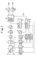
- a video camera with which the present invention may be used is there shown to be similar to that described in the aforementioned application Serial No. 07/393,804.
- Such video camera generally includes a lens system 1 which preferably includes zoom lens elements and an adjustable lens group for focusing the lens system between near and far (infinity) focus conditions.
- the expression "just-focused" means that the lens system is properly focused on an object being imaged.
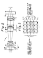
- Lens system 1 is illustrated in FIG. 2 to be comprised of lens groups F1, F2, F3 and F4, wherein lens group F2 constitutes a zoom lens arrangement and lens group F4 constitutes a focus lens system.
- a PN filter 17 is disposed between lens groups F2 and F3, and an adjustable aperture 18, such as an adjustable iris, is illustrated adjacent the PN filter for achieving exposure control.
- An infrared inhibitor 19 serves to remove infrared radiation from the optical image which is focused by the lens system 1 onto an imaging device 2 (Fig. 1)
- Lens group F4 is driven by a focus motor 3 (FIG. 1).
- Iris 18 is driven by an iris motor 4 to increase or decrease the size of the aperture and, thus, the exposure of lens system 1.
- the focus and iris motors 3 and 4 are controlled by a system controller 12 through driver circuits 13 and 14, respectively.
- the system controller 12 receives signals from an iris position detector 5 and a zoom position detector 6 which respectively indicate the positions of the iris 18 and the zoom lens group F2, respectively. The manner in which the system controller 12 operates to adjust the iris 18 and the zoom lens group F4 will be later described.
- the imaging device 2 which is preferably, comprised of a CCD array of the type shown in FIG. 3, is adapted to generate a video signal corresponding to an optical image projected thereon by the lens system 1 as the individual elements which comprise the CCD array are scanned.
- the CCD array is comprised of rows and columns of pixel elements arranged in a complementary-colored checkerboard pattern. This pattern is comprised of successive rows or lines L1, L2, L1, L3, L1, L2, etc., wherein each line L1 is formed of alternating cyan and yellow pixel elements Cy, Ye, Cy, Ye, etc., each line L2 is comprised of alternating green and magenta pixel elements G, M, G, M, etc.
- each line L3 is comprised of alternating magenta and green elements M, G, M, G, etc.
- each row of CCD image pickup device 2 is comprised of 510 pixel elements; and in another embodiment, each row is comprised of 760 pixel elements.
- the pixel elements in a row are scanned successively on a row-by-row basis.
- a scanning clock frequency (8/3)f sc 9.55 MHz.
- each line is comprised of 760 pixel elements
- each scanned pixel element produces a pixel signal level of a magnitude determined by the brightness of the respective point in the image projected on imaging device 2.
- Successive pixel levels in the signal output of the device 2 are sampled by a sample-and-hold circuit 7 and each sample is converted to digital form by an A/D converter 9 after passing through an automatic gain control (AGC) circuit 8.
- the AGC circuit 8 preferably is an analog circuit supplied with a gain setting voltage from system controller 12.
- the system controller 12 includes a microprocessor and produces a digital gain controlling signal which is converted to analog form by a D/A converter 15.
- the complementary colored checkerboard pattern comprising CCD pickup device 2 is scanned or read so that each scan output is comprised of the sum of the pixel level of two vertically adjacent pixel elements, that is, two adjacent rows are read simultaneously. For example, a pixel element in row L1 and a vertically aligned pixel element in row L2 are scanned together, followed by the next pixel element in row L1 and a vertically adjacent or aligned pixel element in row L2. Similarly, when adjacent rows L1 and L3 are scanned together, one pixel element in row L1 is scanned concurrently with a vertically aligned pixel element in row L3. These vertically adjacent pixels are summed and the result thereof is sampled by the sample-and-hold circuit 7.
- A/D converter 9 preferably produces a 10-bit digital signal representing each sample produced by the sample-and-hold circuit 7.
- the digitized samples are supplied from A/D converter 9 to digital video processor 10 and also to an optical detector 11.
- the optical detector 11 generally includes an auto-focus (AF) detection circuit, an auto-exposure (AE) detection circuit and an auto- white balance (AWB) detection circuit, which will be described in greater detail in conjunction with FIG. 4.
- the AF, AE and AWB-detection circuits produce auto-focus, auto-exposure and auto-white balance detection signals, respectively.
- These detection signals are supplied from optical detector 11 to system controller 12 whereat they are used to control driver circuit 13 for the focus motor 3 so as to adjust the focus condition of lens system 1, to control driver circuit 14 for the iris motor 4 and thereby vary the exposure aperture of iris 18 so as to control the exposure condition of the video camera, and to control the digital video processor 10 in accordance with the detected white balance of the image picked up by the video camera.
- System controller 12 also produces the gain setting signal for the AGC circuit 8 in response to the detected exposure level sensed by the optical detector 11.
- Optical detector 11 and system controller 12 are interconnected by way of a serial interface, whereby the AF detection signal, AE detection signal and AWB detection signal produced by optical detector 11 are supplied as AF, AE and AWB control signals by way of a serial output port from the optical detector 11 to the system controller 12; and whereby control signals produced by system controller 12 are applied to the optical detector 11 by way of a serial input port.
- a serial interface reduces the complexity, bulk and weight of the interconnections between the optical detector 11 and the system controller 12.
- the signals communicated between the optical detector and the system controller exhibit a periodicity corresponding to the vertical period intervals of the video signal.
- Digital video signal processor 10 produces luminance and chrominance signals corresponding to the digitized samples supplied thereto by A/D converter 9.
- the manner in which the digital video processor 10 operates forms no part of the present invention per se and, therefore, is not further described herein. Suffice it to say that the digitized luminance and chrominance signals produced by the digital video processor are converted to analog form by D/A converters 15a and 15b, respectively. As a result, analog luminance and chrominance signals are supplied to output terminals 16a and 16b, respectively, from which they may be recorded, displayed or processed further.
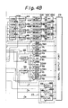
- FIG. 4 there is illustrated a more detailed block diagram of the optical detector 11 which is shown to comprise an auto-focus detector 21, an auto- exposure detector 22 and an auto-white balance detector 23, delineated within broken lines.
- an auto-focus detector 21 an auto-focus detector 21
- an auto-expo detector 22 an auto-expo detector 22
- an auto-white balance detector 23 delineated within broken lines.
- Digital circuits may be used to implement the auto-focus detector 21 in the embodiment of this invention illustrated in FIG. 4.
- the auto-focus detector may be implemented by suitable programming of a microprocessor, as will become apparent from the following description.
- the detector 21 is generally comprised of digital filters which are further described below and are adapted to filter intermediate and higher frequency components from a video signal, selector circuits adapted to select different filtering characteristics from the digital filters as lens group F4 is adjusted to its just-focused position, coring circuits adapted to reject noise signals from the filtered intermediate and higher frequency components, gate circuits adapted to limit the filtered higher frequency components to discrete auto-focus areas of the imaged picture, peak detectors adapted to detect the peaks of the intermediate and higher frequency components derived by the digital filters, and integrators adapted to integrate the detected peaks.
- an input terminal 31 receives a digitized composite video signal, as may be produced by the A/D converter 9 of FIG. 1.
- a luminance separator 32 and a chrominance separator 33 are coupled to input terminal 31 to separate a luminance component Y and chrominance component C R and C B from the digitized composite video signal.
- an auto-focus signal which represents the focus condition of lens system 1 is derived from the separated luminance component Y.
- Such auto-focus signal is produced from the luminance component Y in a discrete area of the video picture being imaged. This discrete area is established by an auto-focus area setting circuit 24 which establishes the focus detection area in which intermediate and higher frequency components of the luminance signal are examined.
- the focus detection area is established by system controller 12 which supplies a suitable control signal to auto-focus area setting circuit 24 by way of a serial input port 28.
- system controller 12 which supplies a suitable control signal to auto-focus area setting circuit 24 by way of a serial input port 28.
- the auto-focus area setting circuit determines when particular pixels included in the focus setting area are scanned.
- an auto-focus area enabling signal is produced. This enabling signal is used as a gating signal, as will be hereinafter described.
- system controller 12 controls auto-focus area setting circuit 24 to establish two or more focus detection areas.
- one focus detection area is a relatively small discrete area AE1 included within a larger discrete area AE2, as shown in FIG. 11A.
- the two discrete focus detection areas may be as illustrated in FIG. 11B, wherein the two areas AE'1 and AE'2 extend laterally across the image and are of substantially equal dimensions, with one area being disposed vertically above the other. It will be appreciated that other focus detection areas may be used and that, if desired, three, four or more focus detection areas may be provided.
- Auto-focus area setting circuit 24 has an output thereof supplied to a selector 30 to which outputs from an auto-exposure area setting circuit 25, an automatic white balance area setting circuit 26 and a display area setting circuit 27 also are supplied.
- the selector 30 is controlled by system controller 12 through the serial input part 28 to couple one of the outputs supplied thereto to an output terminal 47.
- a camera viewfinder (not shown) may display a corresponding area outline. The user of the camera thus may observe the focus detection area which is used by the auto-focus detector 21 to produce the focus detection signal.
- the exposure detection area produced by circuit 25, the white balance detection area produced by circuit 26 or the display area produced by circuit 27 may be observed.
- the video camera may be provided with suitable manual controls (not shown) for causing the system controller 12 to select a desired one of these detection areas for display.
- the checkerboard pattern is scanned so that successive vertical pairs of pixel elements are read.
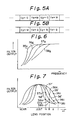
- This successive scanning of pixel pairs produces the signal shown in FIG. 5A when rows L1 and L2 are scanned, and produces the signal shown in FIG. 5B when rows L1 and L3 are scanned.
- FIG. 5A when pixel element Cy in row L1 is scanned concurrently with pixel element G in row L2, the resultant digitized pixel corresponds to a sum signal (Cy + G).
- FIG. 5A represents the summed pixels which are produced as successive pixel pairs in rows L1 and L2 are scanned.
- FIG. 5B represents the successive summed signals produced when pixel pairs in rows L1 and L3 are scanned in succession.
- Chrominance separator 33 operates to subtract successive summed signals produced by the row-by-row scanning of the checkerboard array shown in FIG. 3.
- the digital sample (Cy + G) is subtracted from the digital sample (Ye + M).
- chrominance separator 33 separates the chrominance components C R and C B from the digitized video signal supplied to input terminal 31 from A/D converter 9.
- Luminance separator 32 operates by summing two successive digitized samples produced by the A/D converter. For example, when the samples shown in FIG. 5A are produced, the luminance separator 32 operates to sum these samples as follows: Likewise, the luminance separator 32 operates to sum every two samples of the signal represented by FIG. 5B, as follows:
- separator circuits 32 and 33 convert the sampling frequency at which the digitized luminance and chrominance components are produced. For example, if the checkerboard pattern of FIG. 3 is comprised of 510 pixel elements in each row, the sampling frequency is converted from (8/3)f sc to a re-clocked rate of 2f sc . Alternatively, if the checkerboard pattern is comprised of 760 pixel elements in a row, the sampling frequency is converted from 4f sc to 2f sc .
- the thus separated, digitized luminance signal is supplied from luminance separator 32 to the auto-focus detector 21 and also to the auto-exposure detector 22 and the auto-white balance detector 23.
- the separated chrominance components produced by chrominance separator 33 are supplied to the automatic white balance detector 23.
- the digitized luminance signal Y is supplied to digital filters which serve to separate intermediate and higher frequency components from the luminance signal.
- digital filters which serve to separate intermediate and higher frequency components from the luminance signal.
- intermediate and higher frequency components for example, frequencies which exceed 1 MHz and, preferably, those which exceed 500 KHz.
- the focus condition of the lens may be determined by detecting the amplitude of these intermediate and higher frequency components.
- the expression "higher frequency components" is used hereafter to refer to both the intermediate and higher frequencies.
- the digital filters receiving the digitized luminance signal Y are comprised of a delay circuit 34, conventional filter processors or computers 35, 36 and 37 and a high pass filter circuit 38.
- Delay circuit 34 may be a conventional digital delay line, such as may be formed by cascaded CCD's.
- Each filter processor or computer 35, 36 or 37 is coupled to respective outputs, or taps, of delay circuit 34, and each filter processor or computer is comprised of a summation circuit supplied with individually weighted outputs that are tapped from the delay circuit 34.
- FIG. 6 also graphically represents at 38 a an example of the filtering characteristic of the high pass filter 38. It is seen that the cut-off frequencies of filters 35, 36, 37 and 38 increase successively, as shown in FIG. 6.
- the amplitude, or level, of the higher frequency components included in luminance signal Y is at a maximum when lens group F4 is at its just-focused position, and this amplitude, or level, decreases as the lens moves from that position to increase the extent to which it is unfocused. Accordingly, a relationship may be established between the position of lens group F4 and the amplitude or level of the filtered signals derived from filter processors 35, 36 and 37 and high pass filter 38. This relationship is graphically illustrated in FIG. 7, and it is seen therefrom that the spectral characteristics 35', 36', 37' and 38' of filter processors 35, 36 and 37 and high-pass filter 38, respectively, tend to become “sharper", or more narrowly defined, from filter processor 35 to high pass filter 38. These different filter characteristics are used by auto-focus detector 21 to produce a focus detection signal which may be used to drive lens group F4 accurately and quickly to its just-focused position.
- Selector circuits 39A, 39B, 39C and 39D which may be comprised of suitable digital switches, are controlled by a selection signal produced by system controller 12 and supplied to the selector circuits 39A-39D through serial input port 28.
- each selector circuit includes three inputs a , b and c , any one of which may be selected to be connected to the output thereof.
- Inputs a , b and c of selector circuits 39A and 39B are coupled to the outputs of filter processors 35, 36 and 37, respectively.
- Inputs a , b and c of selector circuits 39C and 39D are coupled to the outputs of filter processors 36 and 37 and of high pass filter 38, respectively.
- a particular filter characteristic may be selected to pass the higher frequency components of the digitized luminance signal Y.
- Coring circuits 40A, 40B, 40C and 40D are coupled to selector circuits 39A, 39B, 39C and 39D, respectively.
- each of the coring circuits 40A-40D is comprised of a threshold detector adapted to detect when the amplitude or level of the higher frequency component supplied thereto from the respective one of the selector circuits 39A-39D exceeds a minimum threshold level. That minimum threshold level is determined for the coring circuits 40A-40D by a suitable control signal supplied thereto from the system controller 12 through the serial input port 28. In the preferred embodiment, this minimum threshold level is approximately equal to the expected noise signal level included in luminance signal Y when the video camera images a scene with relatively little contrast changes therein.
- coring circuits 40A-40D will best be appreciated by referring to the waveform diagrams of FIGS. 8A and 8B.
- the noise signal N which passes through the digital filters 35 may be erroneously detected as a higher frequency component of the luminance signal.
- erroneous detection of the noise signal N may produce a focus detection signal which will be used by system controller 12 to perform an erroneous focus operation.
- a threshold above the expected noise signal level N such as those signal levels which exceed threshold V1 shown in FIG. 8A, erroneous detection of the noise signal level is substantially avoided.
- Coring circuits 40A-40D are supplied with threshold level v1 and thereby detect only the signal levels of the higher frequency components which exceed the level V1. Consequently, noise signals are rejected and substantially only true signal levels of the higher frequency components pass through the coring circuits, as shown in FIG. 8B.
- each of the coring circuits 40A-40D is implemented by a subtractor which subtracts the threshold level V1 from the signal supplied from the respective one of the digital filters. If the threshold level V1 exceeds the signal level from which it is subtracted, the respective coring circuit produces a substantially zero output. Thus, only those higher frequency components which exceed the threshold level pass through the coring circuits 40A-40D.
- threshold level V1 is changed automatically as a function of the intensity of the total light level picked up by imaging device 2.
- this threshold level V1 may be changed manually, as desired.
- coring circuits 40A, 40B, 40C and 40D are selectively supplied through gate circuits 41A, 41B, 41C and 41D and switch circuits 42A, 42B, 42C and 42D to peak detectors 43A, 43B, 43C and 43D, respectively.
- the gate circuits 41A-41D are supplied with gate enabling signals produced by auto-focus area setting circuit 24 to pass only those higher frequency components produced from the pixel elements of the checkerboard pattern that are disposed within the auto-focus area established by setting circuit 24.
- gate circuits 41A and 41B are enabled, or opened, to pass the higher frequency components produced when scanning within larger focus detection area AE2 shown in FIG.
- gate circuits 41C and 41D are enabled to pass the higher frequency components produced from the pixel elements disposed within the smaller focus detection area AE1.
- gate circuits 41A and 41B are used when the lens is relatively far from its just-focused position
- gate circuits 41C and 41D are used when the lens is proximate to its just-focused position.
- Gate circuits 41A-41D are further controlled to respond to a gate inhibit signal generated by auto-focus area setting circuit 24 when the level of the luminance signal Y produced by imaging device 2 is too high.
- a gate inhibit signal generated by auto-focus area setting circuit 24 when the level of the luminance signal Y produced by imaging device 2 is too high.
- auto-focus area setting circuit 24 supplies a gate inhibit signal to gate circuits 41A-41D in the event that the luminance signal Y exceeds a maximum threshold.
- a luminance or brightness detector 46 is coupled to the luminance separator 32 to sense when the magnitude of the luminance signal exceeds a predetermined maximum threshold V2. Hence, the gate circuits 41A-41D are disabled or inhibited for the time period that the luminance signal exceeds this maximum threshold V2.
- FIG. 9A represents the luminance component produced by imaging device 2 and, although analog signal levels are depicted, it will be appreciated that, in actuality, the signal levels are represented in digital form.
- FIG. 9A illustrates an example in which the level of the luminance signal exceeds the maximum threshold V2 during the time T, as will occur when the imaging device images a scene having a very high brightness level, such as a scene that contains an object of high reflectivity, a bright light source, or the like.
- FIG. 9B represents the higher frequency components of the luminance signal of Fig. 9 that pass through one of the digital filters 35, 36, 37 and 38. It will be appreciated that the amplitude of the higher frequency components produced when the luminance signal Y exceeds maximum threshold V2 is quite high and may provide false indications of the focus condition of the lens.
- luminance detector 46 generates an inhibit or masking signal of a duration equal to the time T during which the luminance signal Y exceeds threshold V2.
- This masking signal is supplied to auto-focus area setting circuit 24 which responds thereto to generate a gate inhibit signal by which gate circuits 41A-41D are closed, or inhibited, during this interval; whereby the false higher amplitude components caused by the excessive brightness level in the luminance signal do not pass through the gate circuits.
- This selective operation of the gate circuits is illustrated in FIG. 9D, wherein the gate circuits are inhibited during interval T, that is, the interval during which the luminance signal Y exceeds the maximum threshold V2. Consequently, only the higher frequency components having non-excessive signal levels that are received from the coring circuits 40A-40D are passed by the gate circuits 41A-41D.
- luminance detector 46 may function to sense when the luminance signal Y exceeds maximum threshold V2 and then subtract this luminance signal level from the luminance signal itself, thereby cancelling the excess brightness, whereupon, this "corrected" luminance signal may be supplied to the digital filters for obtaining the higher frequency components.
- Peak detector circuits 43A, 43B, 43C and 43D are coupled to gate circuits 41A, 41B, 41C and 41D by switching circuits 42A, 42B, 42C and 42D, respectively.
- the switching circuits 42A-42D are selectively controlled by system controller 12 which applies suitable switch control signals thereto through serial input port 28.
- Each peak detector circuit although formed as a digital circuit, operates to detect the peak level (that is, the maximum level) in the signal supplied through the switching circuit connected thereto.
- each switching circuit such as, switching circuit 42A, couples the output of the respective gate circuit 41A to peak detector circuit 43A for the duration of a video line interval, whereafter the switching circuit 42A is opened and the peak detector circuit 43A is reset. In this mode of operation, the peak level of the higher frequency components included in the luminance signal Y during each video line interval is detected.
- each switching circuit for example, switching circuit 42A may be closed for an entire vertical field interval.
- the respective peak detector circuit 43A detects the peak (or maximum) level in the higher frequency components included in the luminance signal that is produced during a video field.
- switching circuit 42A is opened and peak detector circuit 43A is reset in preparation to detect the peak level included in the next field interval.
- Each switching circuit such as switching circuit 42A, also is operable to bypass peak detector circuit 43A so as to pass all peaks included in the higher frequency components provided at the output of the respective coring circuit 40A and gate circuit 41A (rather than passing only the maximum peak level included in the higher frequency component).
- Integrator circuits 45A, 45B, 45C and 45D are coupled to peak detector circuits 43A, 43B, 43C and 43D by switching circuits 44A, 44B, 44C and 44D, respectively.
- the switching circuits 44A-44D are controlled by system controller 12 which supplies a control signal thereto through serial input port 28.
- Each of the switching circuits 44A-44D selectively exhibits a first state in which the output of the respective one of the peak detector circuits 43A-43D is coupled to a respective one of the integrator circuits 45A-45D, and a second state in which the respective one of the integrator circuits 45A-45D is bypassed.
- Each of the integrator circuits 45A-45D is adapted to sum the peaks supplied by the respective one of the peak detector circuits 43A-43D connected thereto.
- the peak (or maximum) level sensed by, for example, peak detector circuit 43A in each line of a field interval is summed by integrator circuit 45A to produce a focus detection signal whose magnitude is dependent upon (and, thus, is indicative of) the focus condition of the lens.
- integrator circuit 45A is supplied with the peak, or maximum, level sensed by peak detector circuit 43A in a vertical field interval. The integrator circuit 45A then sums the detected peaks that are sensed in a predetermined number of field intervals, such as the peaks that are detected in four successive field intervals. This too provides a focus detection signal whose magnitude is dependent upon the level of the higher frequency components included in the luminance signal which, in turn, is a function of the focus condition of the lens.
- integrator circuit 45A In the mode of operation of switching circuit 42A for bypassing peak detector circuit 43A, there are supplied to integrator circuit 45A those higher frequency components which exceed threshold V1 established by coring circuit 40A. In that case, integrator circuit 45A sums a number of peak levels included in a field interval, provided those peak levels exceed the threshold V1.
- FIG. 10 is a part schematic, part block diagram of these circuits shown interconnected by switching circuits 42A and 44A which are illustrated as two-position switches.
- switching circuit 42A couples the output of gate 41A to peak detector circuit 43A, and in its second position shown in dotted lines the switching circuit 42A bypasses the peak detector circuit 43A.
- switching circuit 44A is changeable between a first position shown in full lines for coupling the output of peak detector circuit 43A to integrator circuit 45A, and a second position shown in dotted lines to bypass the integrator circuit 45A.
- Switching circuits 42A and 44A are operable by switch control signals supplied thereto through the serial input port 28 from the system controller 12 so as to establish the following modes:
- switching circuits 42A and 44A and their association with the peak detector circuit 43A and integrator circuit 45A have been shown in Fig. 10 and described specifically above, it will be understood that the switching circuits 42B, 42C and 42D and 44B, 44C and 44D are similarly associated with the peak detector circuits 43B, 43C and 43D and integrator circuits 45B, 45C and 45D, respectively.
- the signals provided at the outputs of integrator circuits 45A-45D comprise focus detection signals having magnitudes to which the focus condition of lens group F4 is related.
- Such focus detection signals are supplied by way of serial output port 29 to the system controller 12, which, on the basis thereof, produces a focus control signal supplied by way of driver 13 to focus motor 3 in FIG. 1.
- System controller 12 initially controls selector circuits 39A and 39B so as to select the filtering characteristics exhibited by filter processor or computer 35, and thereby derive the higher frequency components in the luminance signal.
- the selected higher frequency components are applied to gates 41A and 41B through coring circuits 40A and 40B which provide noise rejection in the manner discussed above and shown in FIGS. 8A and 8B.
- the coring circuits 40A and 40B detect signal levels of the higher frequency components which exceed the threshold V1 and supply the detected signals to gates 41A and 41B, respectively.
- auto-focus area setting circuit 24 is controlled by system controller 12 to generate a gate enable signal corresponding to the auto-focus area AE2, shown in FIG. 11A. Accordingly, the detected signal produced by coring circuit 40A is gated to peak detector circuit 43A when the pixel elements of imaging device 2 which are included within auto-focus area AE2 are being scanned. Let it be assumed that peak detector circuit 43A detects the peak (or maximum) level of the detected signal during each video line interval. The detected peaks in those line intervals which are disposed within auto-focus area AE2 are summed in integrator circuit 45A to produce a focus detection signal.
- Coring circuit 40B, gate 41B, peak detector circuit 43B and integrator circuit 45B operate in the same way as just described. Hence, integrator circuit 45B produces a focus detection signal similar to that produced by integrator circuit 45A. Both of these focus detection signals are supplied serially to system controller 12. At this time, the signals that may be produced by integrator circuits 45C and 45D are ignored and, preferably, are not supplied to or utilized by the system controller.
- the focus detection signal produced by one of a pair of integrator circuits is used as a measure of the focus condition of the lens.
- the other focus detection signal for example, the focus detection signal produced by integrator circuit 45B, is used by the system controller 12 to determine when a filter processor having sharper filtering characteristics should be selected. For example, as the lens group F4 is driven toward its just-focused position, the magnitude of the focus detection signal derived by integrator circuit 45B from filter processor 35 changes at a rate which diminishes as the lens approaches its just-focused position. This diminished rate of change is attributed to the decrease in slope of the spectral characteristic 35' of filter processor 35, as illustrated in FIG. 7.
- Coring circuits 40A and 40B now detect the signal levels of the higher frequency components supplied thereto from filter processor 36, and produce detected signals when these signal levels exceed threshold V1.
- Gates 41A and 41B continue to gate the detected signals during the interval corresponding to auto-focus area AE2, and peak detector circuits 43A and 43B detect the peak level in each video line.
- Integrator circuits 45A and 45B sum the peak signal in each line over a field interval to produce the focus detection signals.
- the focus detection signal provided by integrator circuit 45A is used as a measure of the focus condition of the lens
- the focus detection signal provided by integrator circuit 45B is used by the system controller to determine when the filter characteristics should be changed over to a narrower characteristic. Once again, a determination to change over to a narrower filter characteristic is made when the rate of change of the focus detection signal decreases.
- the focus detection signal derived from filter processor 36 increases at a slower rate, as represented by the slope of curve 36' at 36iii.
- the system controller 12 responds thereto by selecting filter processor 37, having the spectral characteristic curve 37' illustrated in FIG. 7, to derive the higher frequency components from the luminance signal Y. More specifically, selector circuits 39A and 39B now are changed over to couple the output of filter processor 37 to the respective coring, gate, peak detector and integrator circuits. These circuits operate in the manner described above to produce the focus detection signals.
- selector circuits 39A and 39B, coring circuits 40A and 40B, gate circuits 41A and 41B, peak detector circuits 43A and 43B and integrator circuits 45A and 45B are used to produce focus detection signals during scanning of the pixel elements within auto-focus area AE2.
- Selector circuits 39C and 39D, coring circuits 40C and 40D, gate circuits 41C and 41D, peak detector circuits 43C and 43D and integrator circuits 45C and 45D are used to produce the focus detection signals during scanning of the pixel elements within auto-focus area AE1.
- auto-focus area setting circuit 24 supplies gate enable signals to at least gate circuits 41A and 41B to define auto-focus area AE2 for a predetermined time.
- the auto-focus area setting circuit supplies gate enable signals to at least gate circuits 41C and 41D to define auto-focus area AE1 (FIG. 11A).
- the outputs of integrator circuits 45A and 45B may be ignored and, if desired, need not even be supplied to system controller 12 through serial output port 29. Alternatively, if these focus detection signals are supplied to the system controller 12, they are not used thereby.
- Selector circuits 39C and 39D are each connected to filter processors 36 and 37 and also to high pass filter 38 and, under the control of system controller 12, they select the spectral characteristics of any one of these filtering circuits in the same manner as selector circuits 39A and 39B select the spectral characteristic of filter processor 35, 36 or 37. For example, let it be assumed that the predetermined time interval, in which the auto-focus area AE2 is defined or being scanned, expires shortly after the focusing lens group F4 reaches position iii on FIG. 7, at which point filter processor 37 was selected by selector circuits 39A and 39B to derive the higher frequency components of the luminance signal.
- System controller 12 now selects selectors 39C and 39D, together with the circuits connected in cascade therewith, to produce the focus detection signals.
- Selectors 39C and 39D are controlled to select filter processor 37 for deriving the higher frequency components.
- Coring circuits 40C and 40D detect signal levels of these higher frequency components which exceed the threshold V1, and gate circuits 41C and 41D gate the detected signals produced by the coring circuits to peak detector circuits 43C and 43D during scanning of pixel elements within auto-focus area AE1.
- Peak detector circuits 43C and 43D detect the peak (or maximum) level in the gated, detected signal during each video line interval, and integrator circuits 45C and 45D sum the detected peaks in the line intervals disposed within auto-focus area AE1.
- integrator circuits 45C and 45D produce focus detection signals in the same manner as discussed above in conjunction with integrator circuits 45A and 45B.
- system controller 12 changes over selector circuits 39C and 39D when the lens arrives at, for example, position iv (shown in FIG. 7). More specifically, the system controller 12 senses that the rate of change of the focus detection signal produced by integrator circuit 45D has decreased and, in response thereto, changes over selector circuits 39C and 39D to select the narrowest spectral characteristic 38' which, in this embodiment, is exhibited by high pass filter 38.
- system controller 12 may sense when the focus detection signal produced by integrator circuit 45C reaches its peak level (rather than reaching a predetermined level), whereupon the focus drive motor 3 is stopped.
- gate circuits 41A-41D are disabled during those periods that such excessive brightness levels are present. More specifically, luminance detector 46 controls auto-focus area setting circuit 24 to produce a gate inhibit signal when excessive brightness levels are sensed, as discussed above in conjunction with FIGS. 9A-9D.
- integrator circuits 45A-45D function to integrate the detected peaks produced by peak detector circuits 43A-43D, except during those intervals when the luminance signal exceeds threshold V2.
- the higher frequency components derived from selector circuits 39A and 39B are used to produce the focus detection signals for a predetermined time, for example, during scanning of pixel elements in the auto-focus area AE2, whereafter the higher frequency components derived by selector circuits 39C and 39D are used to produce the focus detection signals during scanning of pixel elements within auto-focus area AE1.
- selector circuits 39A and 39B may be selected to derive the higher frequency components within auto-focus area AE2 until the rate of change of the focus detection signal produced by integrator circuit 45B is too slow (even after filter processors with narrower spectral characteristics have been selected by selector circuits 39A and 39B).
- selector circuits 39C and 39D are selected for deriving the higher frequency components from which the focus detection signals while scanning pixel elements within auto-focus area AE1 are produced.
- Other techniques may be used to change over from one auto-focus area to another and, accordingly, to change over from one set of selector circuits to another.
- selector circuits 39A and 39B are controlled to select the same filtering characteristics provided by the digital filter and, similarly, selector circuits 39C and 39D also are controlled to select the same filtering characteristics.
- selector circuit 39A may be controlled to select a filter characteristic having broader (or wider) spectral characteristics than the filter characteristic selected by selector circuit 39B.
- selector circuit 39C may be controlled to select a frequency characteristic having broader spectral characteristics than the filter characteristic selected by selector circuit 39D. For example, when the focusing lens is at position i (shown in FIG.
- selector circuit 39A may select the filtering characteristics exhibited by filter processor 35 and represented by the curve 35', whereas selector circuit 39B selects the filtering characteristic exhibited by filter processor 36 and represented by the curve 36'.
- the focus detection signal produced by integrator circuit 45A is derived from filter processor 35 and the focus detection signal produced by integrator circuit 45B is derived from filter processor 36.
- control signals are supplied from the system controller 12 through input port 28 to selector circuits 39A and 39B so that selector circuit 39A now selects the filtering characteristics exhibited by filter processor 36 and selector circuit 39B now selects the filtering characteristics exhibited by filter processor 37.
- selector circuit 39A is changed over to select the filtering characteristics exhibited by filter processor 37.
- selector circuit 39C may be controlled to select the filtering characteristics exhibited by filter processor 36 while selector circuit 39B is controlled to select the filtering characteristics exhibited by filter processor 37.
- selector circuit 39C may be changed over to select the filtering characteristics exhibited by filter processor 37 and selector circuit 39D is changed over to select the filtering characteristics exhibited by high pass filter 38. Further changeovers occur in the selection of the filtering characteristics as the focusing lens approaches its just-focused position, as described above.
- the selector circuits 39A-39D may be controlled so that each selects a respective predetermined filtering characteristic.
- selector circuit 39A may select the filtering characteristic exhibited by filter processor 35
- selector circuit 39B may select the filtering characteristic exhibited by filter processor 36
- selector circuit 39C may select the filtering characteristic exhibited by filter processor 37
- selector circuit 39D may select the filtering characteristic exhibited by high pass filter 38.
- the auto-focus area AE2 is used and gates 41A and 41B are enabled at intervals corresponding to this auto-focus area.
- the focus detection signal from integrator circuit 45A is used by system controller 12 to determine the focus condition of the lens.
- the system controller 12 also senses the rate of change of this focus detection signal and, when that rate decreases, selector circuit 39B is actuated to select the higher frequency components derived from the luminance signal by filter processor 36.
- the focus detection signal produced by integrator circuit 45B is used as an indication of the focus condition of the lens.
- System controller 12 controls selector circuits 39C and 39D in a manner similar to that just described when the focus detection signal is derived from scanning of pixel elements in the auto-focus area AE1.
- a pair of focus detection signals is used as a measure of the focus condition of the lens.
- the focus detection signals produced by integrator circuits 45A and 45B are used in combination to sense the focus condition during scanning of pixel elements within auto-focus area AE2, and the focus detection signals produced by integrator circuits 45C and 45D are used as a measure of the focus condition during scanning of pixel elements within the auto-focus area AE1.
- selector circuit 39A is controlled to select the filtering characteristics exhibited by filter processor 35 while selector circuit 39B is controlled to select the filtering characteristics exhibited by filter processor 36. If an impulse or other interference is present on the focus detection signal produced by integrator circuit 45A, that interference could be erroneously interpreted by the system controller 12 as indicating that the focusing lens is much closer to its just-focused position than it is in fact. Responding to such false interpretation, the system controller may change over selector circuit 39A prematurely to select the filtering characteristics exhibited by filter processor 36 or even filter processor 37.
- the system controller 12 may compare the focus detection signals produced by integrator circuits 45A and 45B to conclude that the higher magnitude of one is not matched by the other and, thus, is artificial. Hence, the system controller 12 may discriminate artifacts, noise or interference superimposed onto a focus detection signal, and thereby avoid false indications of the lens focus condition.
- the lens may be focused quickly and accurately.
- Optimum filtering characteristics are selected as the lens approaches its just-focused position.
- coring circuits 40A-40D prevent erroneous focusing operations that may be attributed to noise signals which pass through the filter processors when a low contrast scene is being imaged.
- focusing errors which otherwise may be due to the imaging of very bright areas are avoided by the brightness detector 46 cooperating with the auto focus area setting circuit 24 for causing the gate circuits 41A-41D to reject the higher frequency components having high amplitudes caused by such bright areas, whereby such higher frequency components having high amplitudes do not influence the focus detection signals produced by integrators 45A-45D.
- Auto-exposure control is effected by suitably opening and closing the iris 18 and by varying the gain of the AGC circuit 8 (Fig. 1) so that the level of the luminance signal from an exposure detection area of the CCD imaging device 2 may be maintained at a predetermined value.
- the overall luminance signal level is substantially elevated and, if the auto-exposure control is effected with reference to such overall luminance signal level, the aperture size of the iris 18 is decreased and a relatively low gain is established for the AGC circuit.
- the output of the video camera would cause objects in the foreground of the corresponding displayed image to appear dark and inconspicuous.
- excessive front-lighting when the scene is subjected to excessive lighting from in front (hereinafter referred to as excessive front-lighting), the brightness level of the background is low relative to the brightness of objects in the foreground and the overall luminance signal level is decreased so that, in response thereto, the iris is opened and the gain of the AGC circuit is increased with the result that the brightly illuminated objects in the foreground of the displayed image would be saturated.
- the above problems encountered in effecting exposure control are avoided by dividing the image of a scene in the field of view of the video camera into a plurality of exposure detection areas whose positions and relative dimensions are controlled in accordance with lighting conditions, such as, normal front-lighting, back-lighting or excessive front lighting, so that at all times exposure control can be effected with reference to a luminance signal level detected for an exposure detection area which contains foreground objects for maintaining a predetermined luminance signal level in respect to such foreground objects.
- lighting conditions such as, normal front-lighting, back-lighting or excessive front lighting
- the detected luminance signal level will be undesirably low.
- the average luminance signal level is approximately 30 percent of the peak level.
- an analog detector circuit has been conventionally provided for detection of the luminance signal level from the CCD imaging device.
- the base of a transistor 101 is connected to an input terminal 100 which receives the luminance signal.
- the collector of the transistor 101 is connected to a power source terminal 109.
- a resistor 102 is connected between the emitter of transistor 101 and the ground.
- the emitter of the transistor 101 is also connected to one end of a resistor 103 which, at its other end, is connected to the base of a transistor 104 and, through a capacitor 105, to ground.
- the collector of transistor 104 is also connected to the power source terminal 109.
- a resistor 107 is connected between the emitter of the transistor 104 and ground, and an output terminal 108 extends from the emitter of the transistor 104.
- a luminance signal from the CCD imaging device is supplied through input terminal 100 to the base of the transistor 101 for detection by the latter, and a detection output from the transistor 101 is extracted at the output terminal 108 through the buffer composed of transistor 104.
- either a characteristic near peak detection or a characteristic near average detection can be established, as desired, by suitably selecting the relationship between the charging time constant and the discharging time constant of the capacitor 105. More specifically, by decreasing the value of the resistor 103, which determines the charging time constant for the capacitor 105, and increasing the value of the resistor 102, which determines the discharging time constant, the characteristic of the detector circuit can be made to approach peak detection. On the other hand, by increasing the value of the resistor 103 and decreasing the value of the resistor 102, the characteristic can be made to approach average detection. Thus, for the described analog detector circuit, the detection characteristic can be readily established.
- the luminance signal from the CCD imaging device is digitized as in the A/D converter 9, and detection of the digital luminance signal level is performed by accumulating luminance signal data within a predetermined area and dividing it by a predetermined coefficient.
- the result of the foregoing is a perfect average detection output which, as earlier noted, is not desirable for auto-exposure control.
- a digital luminance signal level detector circuit is provided with peak detector circuits for detecting peak values of the digital signal and average value detector circuits for detecting average values of the digital signal, and outputs of the peak detector circuits and outputs of the average value detector circuits are suitably weighted and added for desirably indicating a detected luminance signal level that can be advantageously used for auto-exposure control.
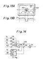
- the luminance component Y from luminance separator 32 is supplied to a so-called "knee" circuit 51 and to one input of a comparator 52.
- a comparison level signal for example, of the level V3 (Fig. 13B), is supplied to another input of the comparator 52 through the serial input port 28 from the system controller 12.
- An output of the filter processor 37 is supplied to peak detector circuits 54A and 54B through gate circuits 53A and 53B, respectively.
- the output of the filter processor 37 which is supplied to gate circuits 53A and 53B is a luminance signal from which a high frequency range noise component has been removed by a low-pass filter.
- the noise component is removed from the luminance component supplied through gate circuits 53A and 53B to peak detector circuits 54A and 54B for accurate detection of the peaks therein.
- both a high-pass filter output, for example, to be applied to the selector circuits 39A-39D, and a low-pass filter output, for example, to be applied to the gate circuits 53A and 53B, can be readily extracted from the filter processor 37.
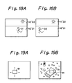
- the gate circuits 53A and 53B are supplied with gate enabling signals supplied from the auto-exposure detection area setting circuit 25 under the control of the system controller 12 for selectively opening and closing the gate circuits 53A and 53B and thereby defining a plurality of exposure detection areas, for example, as at AE21 and AE22 on Figs. 17A and 17B, or as at AE'21 and AE'22 on Figs. 18A and 18B.
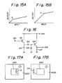
- the knee circuit 51 has a non-linear characteristic, that is, a characteristic comprised of two relatively straight portions with different slopes joined at the knee k1.
- the output of the knee circuit 51 is supplied through gate circuits 55A and 55B to integrator circuits 56A and 56B, respectively.
- the gate circuits 55A and 55B are also supplied with a gate enabling signal from the auto-exposure detection area setting circuit 25 for defining the exposure detection areas AE21 and AE22 or AE'21 and AE'22. It will be apparent that the integrator circuits 56A and 56B detect averages of the luminance signal levels in the digital luminance component Y supplied to the integrator circuits 56A and 56B when the respective gate circuits 55A and 55B are open or enabled.
- the averaged output may be increased by a high brightness occurring at even a relatively small area within the respective exposure detection area, with the result that the auto-exposure control causes the entire picture output by the video camera to have an undesirably dark appearance.
- the gain of the high brightness portion is decreased so that the averaged output is not unduly influenced thereby.
- a characteristic setting signal is supplied from the system controller 12 through the serial input port 28 to the knee circuit 51 for varying the turning point or knee k1 of the characteristic curve thereof, for example, between the positions shown on Figs. 15A and 15B, respectively.
- the comparator 52 detects those samples of the digital luminance component Y from the luminance separator 32 which have levels above the comparison level V3 supplied to the comparator 52 from the system controller 12 through the serial input port 28.
- the resulting comparison output of the comparator 52 is supplied through gate circuits 57A and 57B to distribution detectors 58A and 58B.
- the distribution detectors 58A and 58B count the numbers of samples of the digital luminance signal having levels above the predetermined brightness level V3 during intervals when the gate circuits 57A and 57B are respectively enabled or open.
- the gate circuits 57A and 57B are provided with the gate enabling signals from the auto-exposure detection area setting circuit 25 for defining the exposure detection areas AE21 and AE22 or AE'21 and AE'22.
- the distribution of the luminance signal levels over the scene in the field of view of the video camera can be determined from the outputs of the distribution detectors 58A and 58B.
- the distribution detectors 58A and 58B For example, when a picture or scene in the field of view of the video camera is back-lighted, as illustrated in Fig. 13A, high level luminance signal portions are distributed mostly over the background or peripheral portions of the picture, while relatively low level luminance signal portions, for example, corresponding to a back-lighted object in the foreground of the picture, are distributed mostly in the central portion thereof, as shown in Fig. 13B.
- Such distribution of the high-level luminance signal portions can be determined from the count value constituting the output H1 of the distribution detector 58A and indicating the number of samples having a luminance level above the predetermined level V3, for example, in the exposure detection area AE21, and from the count value constituting the output H2 of the distribution detector 58B and which indicates the number of samples having luminance signal levels above the predetermined level V3, for example, in the exposure detection area AE2.
- Such count values or outputs H1 and H2 from the distribution detectors 58A and 58B are supplied to the system controller 12 through the serial output port 29.
- Outputs P1 and P2 representing luminance signal peak values for the selected exposure detection areas, such as the areas AE21 and AE22, are obtained from the peak detectors 54A and 54B, respectively, and are supplied through the serial output port 29 to the system controller 12.
- outputs IN1 and IN2 representing the integrated values or averages of the luminance signal levels in the selected exposure detection areas, such as the areas AE21 and AE22, respectively are obtained from the integrator circuits 56A and 56B, respectively, and are output through the port 29 to the system controller 12.
- auto-exposure control is effected with reference only to an average of the detected luminance signal levels, for example, as obtained at the outputs IN1, and IN2 of integrator circuits 56A and 56B, the resulting exposure control is defective as the average detected level is undesirably low. Since desirable auto-exposure control is performed with reference to a detected luminance signal level which is nearer to the detected peak luminance signal level than to the average of the detected luminance signal levels, in a preferred embodiment of this invention, auto-exposure control is effected with reference to a detected luminance signal level which is obtained by appropriately mixing average and peak values as derived from the integrator circuits 56A and 56B and from the peak detectors 54A and 54B, respectively.
- the peak values P1 and P2 output by the peak detector circuits 54A and 54B and the average or integrated values IN1 and IN2 output by the integrator circuits 56A and 56B are applied to multipliers 71A, 71B, 72A and 72B, respectively, to be multiplied therein by suitable coefficients.
- the resulting modified or multiplied outputs of the multipliers 71A and 72A are added to each other in an adder 73A, and the outputs of the multipliers 71B and 72B are similarly added to each other in an adder 73B.
- the outputs of the adders 73A and 73B can be provided with detection characteristics that are near to peak detection of the luminance signal levels in the respective exposure detection areas AE21 and AE22, or AE'21 and AE'22.
- the detection levels can be varied. Since these computations are readily carried out by software, the detection levels can be easily changed.
- opening and closing of the iris 18 and changing of the gain of the AGC circuit 8 are suitably controlled.
- the outputs of the adders 73A and 73B are supplied to multipliers 74A and 74B, respectively, and the outputs of the multipliers 74A and 74B are added to each other in an adder 75, with the added output of the latter being applied to the system controller 12 as the exposure detection signal for determining the opening and closing of the iris 18 and the gain of the AGC circuit 8.
- the multipliers 74A and 74B are provided for suitably weighting the detection value of the luminance signal level in one of the exposure detection areas, for example, the central area AE21, and the detection value of the luminance signal level in the other exposure detection area, for example, the peripheral area AE22.
- the weighting of the detection values in the multipliers 74A and 74B, respectively, is desirably dependent on the lighting conditions, for example, on whether the scene in the field of view of the video camera is being subjected to normal forward-lighting, back-lighting or excessive forward-lighting, as determined from the outputs H1 and H2 of the distribution detectors 58A and 58B, respectively.
- the background of the picture is extremely bright relative to objects in the foreground so that luminance signal levels above the predetermined value V3 are mostly distributed in the peripheral exposure detection area AE22 or the upper exposure detection area AE'22.
- the output H2 from the distribution detector 58B is large relative to the output H1 from the distribution detector 58A.
- luminance signal levels above the predetermined value V3 are mostly distributed in the exposure detection area AE21 or AE'21 where the brightly illuminated objects are located, with the result that the output H1 of the distribution detector 58A is then large relative to the output H2 of the distribution detector 58B.
- the outputs H1 and H2 of the distribution detectors 58A and 58B are supplied to a brightness distribution state determining device 76 which, on the basis of a comparison of the outputs H1 and H2 relative to each other, determines whether the scene in the field of view of the video camera is being subjected to normal forward-lighting, back-lighting or excessive forward-lighting and, in response to such determination, provides corresponding outputs to the multipliers 74A and 74B for controlling or varying the coefficients employed therein.
- the coefficient of the multiplier means 74A for weighting the detection luminance signal level of the portion of the picture containing the principal objects is set to a large value
- the coefficient of the multiplier 74B for weighting the detection luminance signal level of the background portion is set to a relatively small value
- the coefficient of multiplier 74A for weighting the brightness of the object portion is set to a relatively small value and the coefficient of the multiplier 74B for weighting the brightness of the background portion is set to a relatively large value.
- the brightness distribution state determining device 76 is effective, in response to the outputs H1 and H2 from the distribution detectors 58A and 58B, to determine the positions and dimensions of the exposure detection areas, that is, to determine whether the exposure detection areas AE21 and AE22 (Figs. 17A and 17B) or the exposure detection areas AE'21 and AE'22 (Figs. 18A and 18B), are to be employed.
- the distribution state determining device 76 provides an output at 76a to the system controller 12 by which the latter selects the arrangement of the exposure detection areas shown in Figs. 18A and 18B, that is, the arrangement in which the image projected on the CCD imaging device 8 is divided into an exposure detection area AE'21 extending laterally across the lower portion of the entire image so as to contain the principal foreground objects, and an exposure detection area AE'22 disposed vertically above the portion AE'21 and also extending across the entire width of the image for containing the background.
- the exposure detection areas AE'21 and AE'22 are selected in response to the normal forward-lighting of the scene, no variation occurs in the brightness as a principal object moves laterally, for example, between the positions O1 and O2 on Figs. 18A and 18B, or in response to panning of the video camera, by reason of the fact that the principal objects remain within the exposure detection area AE'21.
- the distribution state determining device 76 When the scene in the field of view of the video camera is subjected to back-lighting or excessive forward-lighting, the resulting relatively large difference between the outputs H1 and H2 causes the distribution state determining device 76 to provide its output 76a with a level indicating to the system controller 12 that back-lighting or excessive front-lighting has occurred, whereupon the system controller 12 selects the exposure detection areas AE21 and AE22 shown on Figs. 17A and 17B.
- the exposure detection area AE21 which would contain a principal object is located at the center, whereas the exposure detection area AE22 constitutes the peripheral portion and would contain the background.
- the exposure detection area AE21 which would contain a principal object is located at the center
- the exposure detection area AE22 constitutes the peripheral portion and would contain the background.
- the exposure detection area AE21 surrounded by the exposure detection AE22 is of a substantially smaller size than the latter, whereas the exposure detection area AE'21 is of a size that is at least as large as, or even slightly larger than the exposure detection area AE'22. Due to the relatively smaller size of the centrally located exposure detection area AE21, the exposure control effected with the exposure detection areas AE21 and AE22 of Figs. 17A and 17B approximates the desired center-emphasized photometry.
- the output of the brightness distribution state determining device 76 may also be used by the system controller 12 for controlling the turning point or knee k1 of the knee circuit 51. More particularly, when the device 76 determines from the outputs H1 and H2 that the scene in the field of view of the video camera is back-lighted, the turning point k1 is shifted downwardly, for example, to the position shown on Fig. 15A. By reason of such downward shifting of the characteristic curve of the knee circuit 51, the luminance detection signal corresponding to the high brightness of the background due to the back-lighting will be subjected to a reduced gain in the knee circuit 51 so that the resulting exposure control will ensure that objects in the foreground do not appear dark in the back-lighted condition.
- the distribution state detecting device 76 senses from the outputs H1 and H2 that the scene in the field of view of the video camera is subjected to excessive forward-lighting
- the turning point k1 of the knee circuit 51 is raised, for example, to the position shown on Fig. 15B.
- the gain of the knee circuit 51 is increased in respect to the luminance detection signal corresponding to the objects of high brightness appearing in the foreground of the excessively forward-lighted scene.
- the opening of the iris 18 and the gain of the AGC circuit 8 are reduced for ensuring that the principal objects in the foreground of the picture do not saturate when subjected to excessive forward-lighting.
- the gain of the entire control system is set by the brightness distribution state determining device 76, that is, by changing the position of the knee k1 of the knee device 51 as described above, and, as a result thereof, undesirable darkness of a principal object in the foreground of a back-lighted scene, and saturation of principal objects in the foreground of an excessively forward-lighted scene, are avoided.
- White balance control is generally carried out by controlling the levels of red (R), green (G) and blue (B) color signals so as to maintain a predetermined ratio thereof when viewing a white object or area.
- R red
- G green
- B blue
- the fully automatic white balance control performs such control with reference to the integrated value of the entire picture which, for the purposes of the control, is assumed to be white.
- the one-push auto white balance control employs a white balance detection area WB1 (Fig. 19A) which can be varied both in position and dimensions.
- the white balance detection area WB1 can be located on a white part W1 of an object in the scene in the field of view of the video camera, as on Fig. 19B whereupon, in response to actuation or pushing of an auto white balance setting button (not shown), white balance control is carried out on the basis of a signal derived during scanning of the white balance detection area WB1.
- the white balance control can be effected with reference to a white portion of any object, such as, clothes or the like, appearing in the scene in the field of view of the camera. Therefore, it is not necessary to perform white balance adjustment with reference to a white cap or the like inconveniently placed over the lens.
- White balance control with reference to a white portion of an object in the field of view of the video camera ensures more precise white balance adjustment than that achieved when white balance is effected with reference to the integrated value of the entire picture which is assumed to be white.
- a plurality of white balance detection areas may be set or defined, and then the one of those white balance detection areas which approximates a so-called black body radiation curve is selected for actual use in achieving white balance control.
- the luminance signal Y from the Y separator circuit 32 is supplied through a gate circuit 61A to an integrator circuit 62A.
- the chrominance signals C R and C B from the C separator circuit 33 are supplied through gate circuits 61B and 61C to integrator circuits 62B and 62C, respectively.
- Outputs of the integrator circuits 62A, 62B and 62C are supplied, as automatic white balance detection signals, to the system controller 12 through the serial output port 29.
- the gate circuits 61A, 61B and 61C are supplied with gate enabling signals from the automatic white balance detection area setting circuit 26 for defining each white balance detection area.
- the white balance detection area is set by the circuit 26 to be substantially coextensive with the image projected on the CCD imaging device 8.
- the location and dimensions of the white balance detection area WB1 are variably determined and set by the circuit 26 so as to correspond with a white part of the image projected on the CCD imaging device 8.
- the system controller 12 performs the following calculations on the integrated values IN(Y), IN(C R ) and IN(C B ) of the luminance signal Y and the chrominance signals C R and C B , derived from the integrator circuits 62A, 62B and 62C, respectively.
- an integrated value IN(G) of the green (G) color signal is obtained as follows:
- the integrated values of the levels of the three-component color signals R, G and B obtained, as above, in the system controller 12 are communicated through a connection 12 a to the processor 10, and employed in the latter, as in a conventional white balance control circuit, for determining the gains of the respective three-component color signals R, G and B that may be derived from the luminance and chrominance signals at the output terminals 16A and 16B (Fig. 1) so as to maintain a predetermined ratio of the levels of the three-component color signals R, G and B.
- a video camera having digital auto-focus, auto-exposure and auto-white balance controls all under the control of a common system controller with common input and output serial ports which are connected with auto-focus, auto-exposure and auto-white balance sections of a common optical detector circuit.
- the distribution of luminance signal levels is detected from the outputs H1 and H2 of the distribution detectors 58A and 58B, and the nature of the lighting, that is, back-lighting, excessive front-lighting or normal front-lighting, is accurately determined from the outputs H1 and H2 representing the detected distribution of luminance signal levels.
- the positions and dimensions of the exposure detection areas AE21 and AE22 or AE'21 and AE'22 are determined in accordance with the distribution of the luminance signal levels represented by the outputs H1 and H2; the coefficients of the multipliers 74A and 74B are determined in response to the detected distributions of the luminance signal levels represented by the outputs H1 and H2 of the detectors 58A and 58B, respectively, and thereby determine the relative weights given to the sum of the detection signals P1 and IN1 and the sum of the detection signals P2 and IN2 corresponding to the selected exposure detection areas AE21 and AE22 or AE'21 and AE'22, respectively; and the turning point or knee k1 of the knee circuit 51 is determined in accordance with the distribution of the luminance signal levels as represented by
Landscapes
- Engineering & Computer Science (AREA)
- Multimedia (AREA)
- Signal Processing (AREA)
- Physics & Mathematics (AREA)
- General Physics & Mathematics (AREA)
- Automatic Focus Adjustment (AREA)
- Color Television Image Signal Generators (AREA)
- Exposure Control For Cameras (AREA)
Applications Claiming Priority (2)
| Application Number | Priority Date | Filing Date | Title |
|---|---|---|---|
| JP34793/90 | 1990-02-15 | ||
| JP2034793A JP2822256B2 (ja) | 1990-02-15 | 1990-02-15 | ビデオカメラの露光補正装置 |
Publications (3)
| Publication Number | Publication Date |
|---|---|
| EP0446647A2 true EP0446647A2 (fr) | 1991-09-18 |
| EP0446647A3 EP0446647A3 (en) | 1993-01-13 |
| EP0446647B1 EP0446647B1 (fr) | 1997-11-05 |
Family
ID=12424144
Family Applications (1)
| Application Number | Title | Priority Date | Filing Date |
|---|---|---|---|
| EP91102206A Expired - Lifetime EP0446647B1 (fr) | 1990-02-15 | 1991-02-15 | Caméra couleur digitale avec réglage automatique de la mise au point, de l'exposition et de l'équilibre des blancs |
Country Status (5)
| Country | Link |
|---|---|
| US (1) | US5093716A (fr) |
| EP (1) | EP0446647B1 (fr) |
| JP (1) | JP2822256B2 (fr) |
| KR (1) | KR100233480B1 (fr) |
| DE (1) | DE69128101T2 (fr) |
Cited By (11)
| Publication number | Priority date | Publication date | Assignee | Title |
|---|---|---|---|---|
| EP0501723A3 (en) * | 1991-02-27 | 1993-05-19 | Canon Kabushiki Kaisha | Image sensing apparatus provided with a plurality of automatic adjustments using common signal paths |
| EP0546749A3 (en) * | 1991-12-12 | 1993-08-11 | Sony Corporation | Automatic signal control for a solid-state image sensor having multiple output registers |
| EP0572163A3 (fr) * | 1992-05-29 | 1994-01-05 | Sony Corporation | Dispositif de focalisation automatique |
| EP0570968A3 (fr) * | 1992-05-21 | 1994-03-16 | Matsushita Electric Industrial Co Ltd | |
| GB2277656A (en) * | 1993-03-31 | 1994-11-02 | Hitachi Electronics | Control of Television Camera Sensitivity |
| EP0586047A3 (fr) * | 1992-08-27 | 1994-11-17 | Sony Electronics Inc | Focalisation automatique pour caméras. |
| EP0649252A3 (fr) * | 1993-10-15 | 1995-07-19 | Canon Kk | Caméra vidéo utilisant une communication série entre les circuits de commande et de traitement. |
| US8035728B2 (en) | 2008-06-27 | 2011-10-11 | Aptina Imaging Corporation | Method and apparatus providing rule-based auto exposure technique preserving scene dynamic range |
| DE102007027401B4 (de) * | 2006-06-12 | 2012-03-08 | Samsung Electro - Mechanics Co., Ltd. | Vorrichtung zur automatischen Steuerung der Belichtung eines Bildsensors |
| EP2538558A3 (fr) * | 2011-06-21 | 2015-06-03 | Nippon Telegraph And Telephone Corporation | Circuit de commande de gain automatique |
| CN111866483A (zh) * | 2020-07-06 | 2020-10-30 | Oppo广东移动通信有限公司 | 颜色还原方法及装置、计算机可读介质和电子设备 |
Families Citing this family (52)
| Publication number | Priority date | Publication date | Assignee | Title |
|---|---|---|---|---|
| JP3018492B2 (ja) * | 1990-11-28 | 2000-03-13 | ソニー株式会社 | 固体撮像素子の露光調整装置 |
| JP2756197B2 (ja) * | 1991-04-17 | 1998-05-25 | 株式会社三協精機製作所 | 自動合焦装置 |
| JP3163660B2 (ja) * | 1991-07-31 | 2001-05-08 | ソニー株式会社 | カラービデオカメラのホワイトバランス調整装置 |
| US5703638A (en) * | 1991-09-25 | 1997-12-30 | Canon Kabushiki Kaisha | Image pickup apparatus for moving image photographing or for still image photographing |
| JPH05219510A (ja) * | 1992-01-31 | 1993-08-27 | Sony Corp | ビデオ信号処理装置 |
| US5345264A (en) * | 1992-02-27 | 1994-09-06 | Sanyo Electric Co., Ltd. | Video signal processing circuit for a video camera using a luminance signal |
| JP3521920B2 (ja) * | 1992-03-05 | 2004-04-26 | ソニー株式会社 | ビデオカメラ装置 |
| JP3339876B2 (ja) * | 1992-04-28 | 2002-10-28 | 株式会社日立製作所 | 撮像装置 |
| JP3131025B2 (ja) * | 1992-06-08 | 2001-01-31 | キヤノン株式会社 | ビデオカメラ及びその制御方法 |
| JP3106006B2 (ja) * | 1992-06-24 | 2000-11-06 | キヤノン株式会社 | 電子スチルカメラ |
| JP3216022B2 (ja) * | 1992-09-14 | 2001-10-09 | キヤノン株式会社 | 撮像装置 |
| EP0605240B1 (fr) | 1992-12-28 | 2002-05-02 | Canon Kabushiki Kaisha | Circuit intégré monopuce pour dispositif de commande de focalisation |
| KR100396203B1 (ko) * | 1993-06-17 | 2003-12-31 | 소니 가부시끼 가이샤 | 노광장치및방법,그노광장치를가지는비디오카메라 |
| JP3696895B2 (ja) * | 1993-06-21 | 2005-09-21 | キヤノン株式会社 | ビデオカメラ及び映像信号処理方法 |
| US5576838A (en) * | 1994-03-08 | 1996-11-19 | Renievision, Inc. | Personal video capture system |
| EP0679021B1 (fr) * | 1994-04-19 | 2010-12-15 | Eastman Kodak Company | Caméra à contrôle automatique d'exposition avec capteur CCD à indice d'exposition variable |
| US5764291A (en) * | 1994-09-30 | 1998-06-09 | Apple Computer, Inc. | Apparatus and method for orientation-dependent camera exposure and focus setting optimization |
| US6222587B1 (en) * | 1995-06-14 | 2001-04-24 | Sony Corporation | Focus control method and video camera |
| JP3697745B2 (ja) * | 1995-06-30 | 2005-09-21 | ソニー株式会社 | オートフォーカス制御装置及び方法 |
| US5745175A (en) * | 1995-10-02 | 1998-04-28 | Flashpoint Technologies, Inc. | Method and system for providing automatic focus control for a still digital camera |
| US6885994B1 (en) | 1995-12-26 | 2005-04-26 | Catalina Marketing International, Inc. | System and method for providing shopping aids and incentives to customers through a computer network |
| JPH09284784A (ja) * | 1996-04-12 | 1997-10-31 | Sony Corp | カラー撮像装置 |
| JP3107760B2 (ja) * | 1996-12-25 | 2000-11-13 | 松下電器産業株式会社 | 露光量制御装置 |
| US6137533A (en) * | 1997-05-14 | 2000-10-24 | Cirrus Logic, Inc. | System and method for enhancing dynamic range in images |
| US5973734A (en) | 1997-07-09 | 1999-10-26 | Flashpoint Technology, Inc. | Method and apparatus for correcting aspect ratio in a camera graphical user interface |
| US6317141B1 (en) | 1998-12-31 | 2001-11-13 | Flashpoint Technology, Inc. | Method and apparatus for editing heterogeneous media objects in a digital imaging device |
| JP3897481B2 (ja) * | 1999-06-04 | 2007-03-22 | キヤノン株式会社 | カメラ及びその制御方法 |
| JP3302003B2 (ja) * | 2000-03-08 | 2002-07-15 | 三洋電機株式会社 | オートフォーカス機能を有する撮像装置 |
| JP3615462B2 (ja) * | 2000-05-12 | 2005-02-02 | 三洋電機株式会社 | 自動露光調節カメラ |
| US6785414B1 (en) | 2000-09-28 | 2004-08-31 | Media Cybernetics, Inc. | System and method for establishing an aggregate degree of brightness for each primary color to create a composite color digital image |
| JP2002323649A (ja) * | 2001-04-26 | 2002-11-08 | Hitachi Ltd | 撮像装置 |
| US6529235B1 (en) * | 2002-03-21 | 2003-03-04 | Sunplus Technology Co., Ltd. | Auto white balance apparatus and method in a digital camera with a strobe |
| JP3937924B2 (ja) * | 2002-05-23 | 2007-06-27 | キヤノン株式会社 | 撮像装置及びその制御方法 |
| US7369712B2 (en) * | 2003-09-30 | 2008-05-06 | Fotonation Vision Limited | Automated statistical self-calibrating detection and removal of blemishes in digital images based on multiple occurrences of dust in images |
| US7340109B2 (en) * | 2003-09-30 | 2008-03-04 | Fotonation Vision Limited | Automated statistical self-calibrating detection and removal of blemishes in digital images dependent upon changes in extracted parameter values |
| US7308156B2 (en) * | 2003-09-30 | 2007-12-11 | Fotonation Vision Limited | Automated statistical self-calibrating detection and removal of blemishes in digital images based on a dust map developed from actual image data |
| US7424170B2 (en) | 2003-09-30 | 2008-09-09 | Fotonation Vision Limited | Automated statistical self-calibrating detection and removal of blemishes in digital images based on determining probabilities based on image analysis of single images |
| US7310450B2 (en) | 2003-09-30 | 2007-12-18 | Fotonation Vision Limited | Method of detecting and correcting dust in digital images based on aura and shadow region analysis |
| US7676110B2 (en) * | 2003-09-30 | 2010-03-09 | Fotonation Vision Limited | Determination of need to service a camera based on detection of blemishes in digital images |
| US7295233B2 (en) * | 2003-09-30 | 2007-11-13 | Fotonation Vision Limited | Detection and removal of blemishes in digital images utilizing original images of defocused scenes |
| US8369650B2 (en) | 2003-09-30 | 2013-02-05 | DigitalOptics Corporation Europe Limited | Image defect map creation using batches of digital images |
| US7590305B2 (en) | 2003-09-30 | 2009-09-15 | Fotonation Vision Limited | Digital camera with built-in lens calibration table |
| WO2007095556A2 (fr) | 2006-02-14 | 2007-08-23 | Fotonation Vision Limited | Dispositif d'acquisition d'image numérique comportant une fonction intégrée de détection et de cartographie de poussières |
| US20080052026A1 (en) * | 2006-08-23 | 2008-02-28 | Qurio Holdings, Inc. | Configuring a content capture device for one or more service providers |
| US9224145B1 (en) | 2006-08-30 | 2015-12-29 | Qurio Holdings, Inc. | Venue based digital rights using capture device with digital watermarking capability |
| US20080251575A1 (en) * | 2007-04-13 | 2008-10-16 | Yourday, Inc. | System for capturing and managing personalized video images over an ip-based control and data local area network |
| WO2009041918A1 (fr) * | 2007-09-26 | 2009-04-02 | Agency For Science, Technology And Research | Procédé et système pour générer une image entièrement bien focalisée d'une grande scène tridimensionnelle |
| US20100259639A1 (en) * | 2009-04-13 | 2010-10-14 | Qualcomm Incorporated | Automatic backlight detection |
| US8743235B2 (en) | 2009-11-04 | 2014-06-03 | Board Of Regents, The University Of Texas System | Adaptive automatic exposure apparatus and method for digital images |
| US8215557B1 (en) * | 2010-11-18 | 2012-07-10 | Innovation Associates, Inc. | Low profile color-based counting system |
| JP6146293B2 (ja) * | 2013-12-25 | 2017-06-14 | ソニー株式会社 | 制御装置、制御方法および制御システム |
| RU2667790C1 (ru) | 2017-09-01 | 2018-09-24 | Самсунг Электроникс Ко., Лтд. | Способ автоматической регулировки экспозиции для инфракрасной камеры и использующее этот способ вычислительное устройство пользователя |
Family Cites Families (11)
| Publication number | Priority date | Publication date | Assignee | Title |
|---|---|---|---|---|
| US4814861A (en) * | 1985-07-10 | 1989-03-21 | Canon Kabushiki Kaisha | Signal processing apparatus with independent gain control for chrominance and color signals |
| JP2568515B2 (ja) * | 1986-09-01 | 1997-01-08 | 松下電器産業株式会社 | 撮像装置 |
| US4843476A (en) * | 1986-11-25 | 1989-06-27 | Matsushita Electric Industrial Co., Ltd. | System for controlling the amount of light reaching an image pick-up apparatus based on a brightness/darkness ratio weighing |
| JPH07114474B2 (ja) * | 1987-01-05 | 1995-12-06 | 株式会社東芝 | 電子スチルカメラ |
| JPS6489884A (en) * | 1987-09-30 | 1989-04-05 | Sony Corp | White balance correction circuit |
| AU607033B2 (en) * | 1988-01-12 | 1991-02-21 | Sanyo Electric Co., Ltd. | Auto iris/gamma correction apparatus for making automatic exposure adjustment and/or automatic gamma correction in response to video signal and image sensing apparatus comprising such auto iris/gamma correction apparatus |
| JP2898987B2 (ja) * | 1988-03-18 | 1999-06-02 | キヤノン株式会社 | 露光制御装置 |
| US4969045A (en) * | 1988-05-20 | 1990-11-06 | Sanyo Electric Co., Ltd. | Image sensing apparatus having automatic iris function of automatically adjusting exposure in response to video signal |
| US4998162A (en) * | 1988-08-22 | 1991-03-05 | Sony Corporation | Video camera |
| US4887121A (en) * | 1988-12-12 | 1989-12-12 | Eastman Kodak Company | Method and apparatus for exposure control based on color balance information |
| JPH031772A (ja) * | 1989-05-30 | 1991-01-08 | Sony Corp | 撮像装置 |
-
1990
- 1990-02-15 JP JP2034793A patent/JP2822256B2/ja not_active Expired - Lifetime
-
1991
- 1991-02-01 US US07/653,364 patent/US5093716A/en not_active Expired - Lifetime
- 1991-02-13 KR KR1019910002481A patent/KR100233480B1/ko not_active Expired - Lifetime
- 1991-02-15 EP EP91102206A patent/EP0446647B1/fr not_active Expired - Lifetime
- 1991-02-15 DE DE69128101T patent/DE69128101T2/de not_active Expired - Lifetime
Cited By (19)
| Publication number | Priority date | Publication date | Assignee | Title |
|---|---|---|---|---|
| EP1043889A1 (fr) * | 1991-02-27 | 2000-10-11 | Canon Kabushiki Kaisha | Appareil de détection d'images muni de plusieurs réglages automatiques utilisant des trajets de signaux communs |
| US6353488B1 (en) | 1991-02-27 | 2002-03-05 | Canon Kabushiki Kaisha | Image sensing apparatus having common circuitry for processing digital adjustment signals |
| EP0501723A3 (en) * | 1991-02-27 | 1993-05-19 | Canon Kabushiki Kaisha | Image sensing apparatus provided with a plurality of automatic adjustments using common signal paths |
| US5585844A (en) * | 1991-02-27 | 1996-12-17 | Canon Kabushiki Kaisha | Image sensing apparatus having common circuitry for processing digital adjustment signals |
| EP0546749A3 (en) * | 1991-12-12 | 1993-08-11 | Sony Corporation | Automatic signal control for a solid-state image sensor having multiple output registers |
| US5671015A (en) * | 1991-12-12 | 1997-09-23 | Sony Corporation | Signal processing apparatus |
| US5703644A (en) * | 1992-05-21 | 1997-12-30 | Matsushita Electric Industrial Co., Ltd. | Automatic exposure control apparatus |
| EP0570968A3 (fr) * | 1992-05-21 | 1994-03-16 | Matsushita Electric Industrial Co Ltd | |
| US5982430A (en) * | 1992-05-29 | 1999-11-09 | Sony Corporation | Auto focus apparatus |
| EP0572163A3 (fr) * | 1992-05-29 | 1994-01-05 | Sony Corporation | Dispositif de focalisation automatique |
| US5539462A (en) * | 1992-08-27 | 1996-07-23 | Sony Corporation | Camera auto focus system with detector circuits for generating evaluation functions |
| EP0586047A3 (fr) * | 1992-08-27 | 1994-11-17 | Sony Electronics Inc | Focalisation automatique pour caméras. |
| GB2277656A (en) * | 1993-03-31 | 1994-11-02 | Hitachi Electronics | Control of Television Camera Sensitivity |
| EP0649252A3 (fr) * | 1993-10-15 | 1995-07-19 | Canon Kk | Caméra vidéo utilisant une communication série entre les circuits de commande et de traitement. |
| US6469736B1 (en) | 1993-10-15 | 2002-10-22 | Canon Kabushiki Kaisha | Video camera with integrated signal processing |
| DE102007027401B4 (de) * | 2006-06-12 | 2012-03-08 | Samsung Electro - Mechanics Co., Ltd. | Vorrichtung zur automatischen Steuerung der Belichtung eines Bildsensors |
| US8035728B2 (en) | 2008-06-27 | 2011-10-11 | Aptina Imaging Corporation | Method and apparatus providing rule-based auto exposure technique preserving scene dynamic range |
| EP2538558A3 (fr) * | 2011-06-21 | 2015-06-03 | Nippon Telegraph And Telephone Corporation | Circuit de commande de gain automatique |
| CN111866483A (zh) * | 2020-07-06 | 2020-10-30 | Oppo广东移动通信有限公司 | 颜色还原方法及装置、计算机可读介质和电子设备 |
Also Published As
| Publication number | Publication date |
|---|---|
| JP2822256B2 (ja) | 1998-11-11 |
| KR910016190A (ko) | 1991-09-30 |
| JPH03238980A (ja) | 1991-10-24 |
| EP0446647A3 (en) | 1993-01-13 |
| DE69128101D1 (de) | 1997-12-11 |
| KR100233480B1 (ko) | 1999-12-01 |
| US5093716A (en) | 1992-03-03 |
| DE69128101T2 (de) | 1998-03-05 |
| EP0446647B1 (fr) | 1997-11-05 |
Similar Documents
| Publication | Publication Date | Title |
|---|---|---|
| US5093716A (en) | Digital color video camera with auto-focus, auto-exposure and auto-white balance, and an auto exposure system therefor which compensates for abnormal lighting | |
| US5235428A (en) | Auto-focus system for video camera | |
| US5182636A (en) | Color video camera with auto-white balance control | |
| JP4149528B2 (ja) | 自動焦点検出装置 | |
| US4998162A (en) | Video camera | |
| KR100220764B1 (ko) | 촬상 장치 | |
| US5640635A (en) | System and method for automatic engagement of a close-up lens in a fixed-focus camera | |
| US5144450A (en) | Auto focus frequency conversion filter for ccd imagers having different numbers of pixels | |
| EP0721280B1 (fr) | Système de mise au point automatique pour caméra vidéo | |
| KR100220011B1 (ko) | 출력 화면과 연동된 포커스 평가치를 검출하는 카메라 장치 | |
| KR0126453B1 (ko) | 자동 노출 제어장치 | |
| JP3517423B2 (ja) | 自動焦点調節装置 | |
| US5835143A (en) | Automatic focusing system for a still video camera | |
| JPH08107560A (ja) | 画像入力装置 | |
| KR19980080516A (ko) | 자동-아이리스 제어에 사용되는 선명도 정보를 용이하게 추출가능한 비디오 카메라 장치 | |
| JP2979567B2 (ja) | ビデオカメラの露光補正装置 | |
| JPH03243072A (ja) | オートフォーカス回路 | |
| JP2860996B2 (ja) | 撮像装置 | |
| KR100287199B1 (ko) | 자동초점조절장치 및 그 방법 | |
| JPH05103250A (ja) | 撮像装置 | |
| KR100275678B1 (ko) | 다중노출영상을 이용한 포커싱방법 및 그 장치 | |
| JPH0263292A (ja) | 撮像装置 | |
| JP3063097B2 (ja) | 撮像装置 | |
| JPH03238981A (ja) | ディジタル信号レベル検出回路 | |
| JPH03232392A (ja) | 白バランス調整装置 |
Legal Events
| Date | Code | Title | Description |
|---|---|---|---|
| PUAI | Public reference made under article 153(3) epc to a published international application that has entered the european phase |
Free format text: ORIGINAL CODE: 0009012 |
|
| AK | Designated contracting states |
Kind code of ref document: A2 Designated state(s): DE FR GB |
|
| PUAL | Search report despatched |
Free format text: ORIGINAL CODE: 0009013 |
|
| AK | Designated contracting states |
Kind code of ref document: A3 Designated state(s): DE FR GB |
|
| 17P | Request for examination filed |
Effective date: 19930713 |
|
| 17Q | First examination report despatched |
Effective date: 19950526 |
|
| GRAG | Despatch of communication of intention to grant |
Free format text: ORIGINAL CODE: EPIDOS AGRA |
|
| GRAH | Despatch of communication of intention to grant a patent |
Free format text: ORIGINAL CODE: EPIDOS IGRA |
|
| GRAH | Despatch of communication of intention to grant a patent |
Free format text: ORIGINAL CODE: EPIDOS IGRA |
|
| GRAA | (expected) grant |
Free format text: ORIGINAL CODE: 0009210 |
|
| AK | Designated contracting states |
Kind code of ref document: B1 Designated state(s): DE FR GB |
|
| REF | Corresponds to: |
Ref document number: 69128101 Country of ref document: DE Date of ref document: 19971211 |
|
| ET | Fr: translation filed | ||
| PLBE | No opposition filed within time limit |
Free format text: ORIGINAL CODE: 0009261 |
|
| STAA | Information on the status of an ep patent application or granted ep patent |
Free format text: STATUS: NO OPPOSITION FILED WITHIN TIME LIMIT |
|
| 26N | No opposition filed | ||
| REG | Reference to a national code |
Ref country code: GB Ref legal event code: IF02 |
|
| PGFP | Annual fee paid to national office [announced via postgrant information from national office to epo] |
Ref country code: FR Payment date: 20100226 Year of fee payment: 20 |
|
| PGFP | Annual fee paid to national office [announced via postgrant information from national office to epo] |
Ref country code: DE Payment date: 20100219 Year of fee payment: 20 Ref country code: GB Payment date: 20100218 Year of fee payment: 20 |
|
| REG | Reference to a national code |
Ref country code: DE Ref legal event code: R071 Ref document number: 69128101 Country of ref document: DE |
|
| REG | Reference to a national code |
Ref country code: GB Ref legal event code: PE20 Expiry date: 20110214 |
|
| PG25 | Lapsed in a contracting state [announced via postgrant information from national office to epo] |
Ref country code: GB Free format text: LAPSE BECAUSE OF EXPIRATION OF PROTECTION Effective date: 20110214 |
|
| PG25 | Lapsed in a contracting state [announced via postgrant information from national office to epo] |
Ref country code: DE Free format text: LAPSE BECAUSE OF EXPIRATION OF PROTECTION Effective date: 20110215 |