EP0446814A2 - Nonreducing dielectric ceramic composition - Google Patents
Nonreducing dielectric ceramic composition Download PDFInfo
- Publication number
- EP0446814A2 EP0446814A2 EP91103610A EP91103610A EP0446814A2 EP 0446814 A2 EP0446814 A2 EP 0446814A2 EP 91103610 A EP91103610 A EP 91103610A EP 91103610 A EP91103610 A EP 91103610A EP 0446814 A2 EP0446814 A2 EP 0446814A2
- Authority
- EP
- European Patent Office
- Prior art keywords
- dielectric
- sample
- ceramic composition
- dielectric ceramic
- ceramics
- Prior art date
- Legal status (The legal status is an assumption and is not a legal conclusion. Google has not performed a legal analysis and makes no representation as to the accuracy of the status listed.)
- Granted
Links
Classifications
-
- H—ELECTRICITY
- H01—ELECTRIC ELEMENTS
- H01G—CAPACITORS; CAPACITORS, RECTIFIERS, DETECTORS, SWITCHING DEVICES, LIGHT-SENSITIVE OR TEMPERATURE-SENSITIVE DEVICES OF THE ELECTROLYTIC TYPE
- H01G4/00—Fixed capacitors; Processes of their manufacture
- H01G4/002—Details
- H01G4/018—Dielectrics
- H01G4/06—Solid dielectrics
- H01G4/08—Inorganic dielectrics
- H01G4/12—Ceramic dielectrics
- H01G4/1209—Ceramic dielectrics characterised by the ceramic dielectric material
- H01G4/1236—Ceramic dielectrics characterised by the ceramic dielectric material based on zirconium oxides or zirconates
- H01G4/1245—Ceramic dielectrics characterised by the ceramic dielectric material based on zirconium oxides or zirconates containing also titanates
-
- C—CHEMISTRY; METALLURGY
- C04—CEMENTS; CONCRETE; ARTIFICIAL STONE; CERAMICS; REFRACTORIES
- C04B—LIME, MAGNESIA; SLAG; CEMENTS; COMPOSITIONS THEREOF, e.g. MORTARS, CONCRETE OR LIKE BUILDING MATERIALS; ARTIFICIAL STONE; CERAMICS; REFRACTORIES; TREATMENT OF NATURAL STONE
- C04B35/00—Shaped ceramic products characterised by their composition; Ceramics compositions; Processing powders of inorganic compounds preparatory to the manufacturing of ceramic products
- C04B35/01—Shaped ceramic products characterised by their composition; Ceramics compositions; Processing powders of inorganic compounds preparatory to the manufacturing of ceramic products based on oxide ceramics
- C04B35/48—Shaped ceramic products characterised by their composition; Ceramics compositions; Processing powders of inorganic compounds preparatory to the manufacturing of ceramic products based on oxide ceramics based on zirconium or hafnium oxides, zirconates, zircon or hafnates
- C04B35/49—Shaped ceramic products characterised by their composition; Ceramics compositions; Processing powders of inorganic compounds preparatory to the manufacturing of ceramic products based on oxide ceramics based on zirconium or hafnium oxides, zirconates, zircon or hafnates containing also titanium oxides or titanates
Definitions
- an electrostatic capacity (c) and a dielectric loss (tan ⁇ ) were measured at the condition of 1KHz and 1 V rms using an automatic bridge.
- the insulation resistance (R) was taken a value measured by a high insulation resistance tester after applying the DC voltage of 500V for two minutes.
- the insulation resistance was measured at 25 o C and 85 o C and logarithms (log ⁇ ) of respective resistivities were calculated.
- the crystal grain diameter of the sample was evaluated by observing the sample surface with an electron microscope. The measured results are shown in Table 2.
Landscapes
- Engineering & Computer Science (AREA)
- Chemical & Material Sciences (AREA)
- Ceramic Engineering (AREA)
- Power Engineering (AREA)
- Manufacturing & Machinery (AREA)
- Microelectronics & Electronic Packaging (AREA)
- Inorganic Chemistry (AREA)
- Composite Materials (AREA)
- Materials Engineering (AREA)
- Structural Engineering (AREA)
- Organic Chemistry (AREA)
- Compositions Of Oxide Ceramics (AREA)
- Inorganic Insulating Materials (AREA)
- Ceramic Capacitors (AREA)
Abstract
Description
- The present invention relates to a nonreducing dielectric ceramic composition, and particularly, to a nonreducing dielectric ceramic composition used, for example, in a monolithic ceramic capicitor and the like.
- For manufacturing monolithic ceramic capacitors, first, a dielectric material sheet coated with an electrode material which serves as an internal electrode thereon is prepared. As the dielectric material, a material having BaTiO₃ as the main component is used. Dielectric ceramics having the internal electrode is obtained by pressing the the stacked dielectric materials coated with the electrode material into a monolithic multi-layer body, which is fired in a natural atmosphere at 1250 to 1350oC. Then, on edge faces of the dielectric ceramics an external electrode conducting with the internal electrode is baked to obtain the monolithic ceramic capacitor.
- Accordingly, as the material of the internal electrode, the following conditions must be satisfied.
- (a) Since the dielectric ceramics and the internal electrode are baked simultaneously, the melting point must be higher than firing temperature of the dielectric material.
- (b) must not oxidize even in an oxidizing atmosphere, and not react with the dielectric material.
- As the electrode material which satisfies such conditions, nobel metals such as platinum, gold, palladium or their are used in the past.
- However, while these electrode materials have superior characteristics, they were very expensive. Therefore, the cost of electrode material involved in the monolithic ceramic capacitor reaches 30 to 70% of the whole cost of the capacitor, has become the biggest factor in raising the manufacturing cost.
- Though, besides the nobel metals, there are base metals such as Ni, Fe, Co, W and Mo which have a high melting point, these base metals are liable to oxidize in a oxidizing atmosphere and do not function as the electrode. Accordingly, in order to use these base metals as the internal electrode of the monolithic ceramic capacitor, they must be fired in the neutral or reducing atmosphere together with the dielectric material. In the conventional dielectric ceramic material, however, when fired in the reducing atmosphere, they are reduced remarkably and become semiconductive.
- In order to conquer such defects, as shown, for example, in Japanese Patent Publication No. 42588/82 and the U.S. Patent No. 4,115, 493, a dielectric material whose ratio of Ba site/Ti site is above the stoichiometric ratio in a barium titanate solid solution was devised. By using such dielectric material, the dielectric ceramics which does not become semiconductive even when fired in the reducing atmosphere was obtained to enable manufacturing of the monolithic ceramic capacitor, using the base metal such as nickel and the like as the internal electrode.
- With development of electronics in recent years, miniaturization of electronic components has progressed rapidly, results in a trend to miniaturize also the monolithic ceramic capacitor.
- As a method of miniaturizing the monolithic ceramic capacitor, generally, a dielectric layer is formed into a thin film, when the thickness of the thin film is below 10 m, the number of crystal grains is reduced in one layer of ceramic sheet, so that the reliability of the monolithic ceramic capacitor is deteriorated.
- It is, therefore, a primary object of the present invention to provide a nonreducing dielectric ceramic composition which does not become semiconductive even when fired in a reducing atmosphere, and enables miniaturization of a monolithic ceramic capacitor when used.
- The present invention is directed to the nonreducing dielectric ceramic composition whose main component is consisting of respective oxides of Ba, Ca, Mg, Sr, Ce, Ti and Zr, represented by the following general formula, (Ba1-ℓ -m-n-oSrℓCamMgnCeo)q(Ti1-pZrp)O₃, where ℓ, m, n, o, p and q satisfying 0.05 ≦ ℓ ≦ 0.30, 0.005 ≦ m ≦ 0.22, 0.0005 ≦ n ≦ 0.05, 0.0005 ≦ o ≦ 0.02, 0 < p ≦ 0.20, 1.002 ≦ q ≦ 1.03, and for the main component of 100 mole %, at least one of respective oxides is added by 0.02 to 2.0 mole %, when the respective oxides of Mn, Fe, Cr and Co are represented as MnO₂, Fe₂O₃, Cr₂O₃ and CoO.
- According to the present invention, the nonreducing dielectric ceramic composition which does not reduce and become semiconductive even when fired in a nonreducing atmosphere can be obtained. Accordingly, when this nonreducing dielectric ceramic composition is used for manufacturing a monolithic ceramic capacitor, base metals may be used as an electrode material thus cost of the monolithic ceramic capacitor can be reduced.
- In ceramics using the nonreducing dielectric ceramic composition, as compared with the case using a conventional dielectric composition, its crystal grains can be minimized. Thus, when manufacturing the monolithic ceramic capacitor, even when a dielectric layer is formed into a thin film, the quantity of crystal grains in the layer does not reduce as the conventional monolithic ceramic capacitor. Therefore, the monolithic ceramic capacitor which is high reliablity and possible to be miniaturized can be obtained.
- The above and other objects, features, aspects and advantages of the present invention will become more apparent from the following detailed description of the embodiments.
- First, as raw materials, BaCo₃, SrCO₃, MgCO₃, CeO₂, TiO₂, ZrO₂, MnO₂, Fe₂O₃, CrO₂, CoO having the purity above 99.8% were prepared. These raw materials were weighed to obtain a final sample represented by a composition formula, (Ba1-ℓ-m-n-oSrℓCamMgnCeo)q(ti1-pZrp)O₃, where proportions of ℓ, m, n, o, p, and q were as shown in Table 1. The weighed raw material was subjected to wet mixing in a ball-mill, dried after pulverized and calcined for two hours in air at 1100oC to obtain a calcined product. To the calcined powder, a mixed aqueous solution consisting of an organic binder, a dispersant and a defoaming agent of 15% by weight was added and mixed in a ball-mill with water of 50% by weight, then pulverized to prepare a slurry.
- The slurry was introduced into a doctor blade to form a green sheet. The green sheets were laminated and pressed into stacked body. Thus obtained stacked body was punched to obtain a disc having 10mm diameter and 1mm thickness. The resulting disc was heated to 500oC in air to burn the organic binder, then fired for two hours at 1250 to 1350oC in a reducing atmospheric oven filled with H₂-N₂-air gases of 3 x 10⁻⁸ to 3 x 10⁻¹⁰ atm oxygen partial pressure to obtain a sintered body. The resulting sintered body was coated with In-Ga alloy on its both of main surfaces to prepare a sample for measuring characteristics.
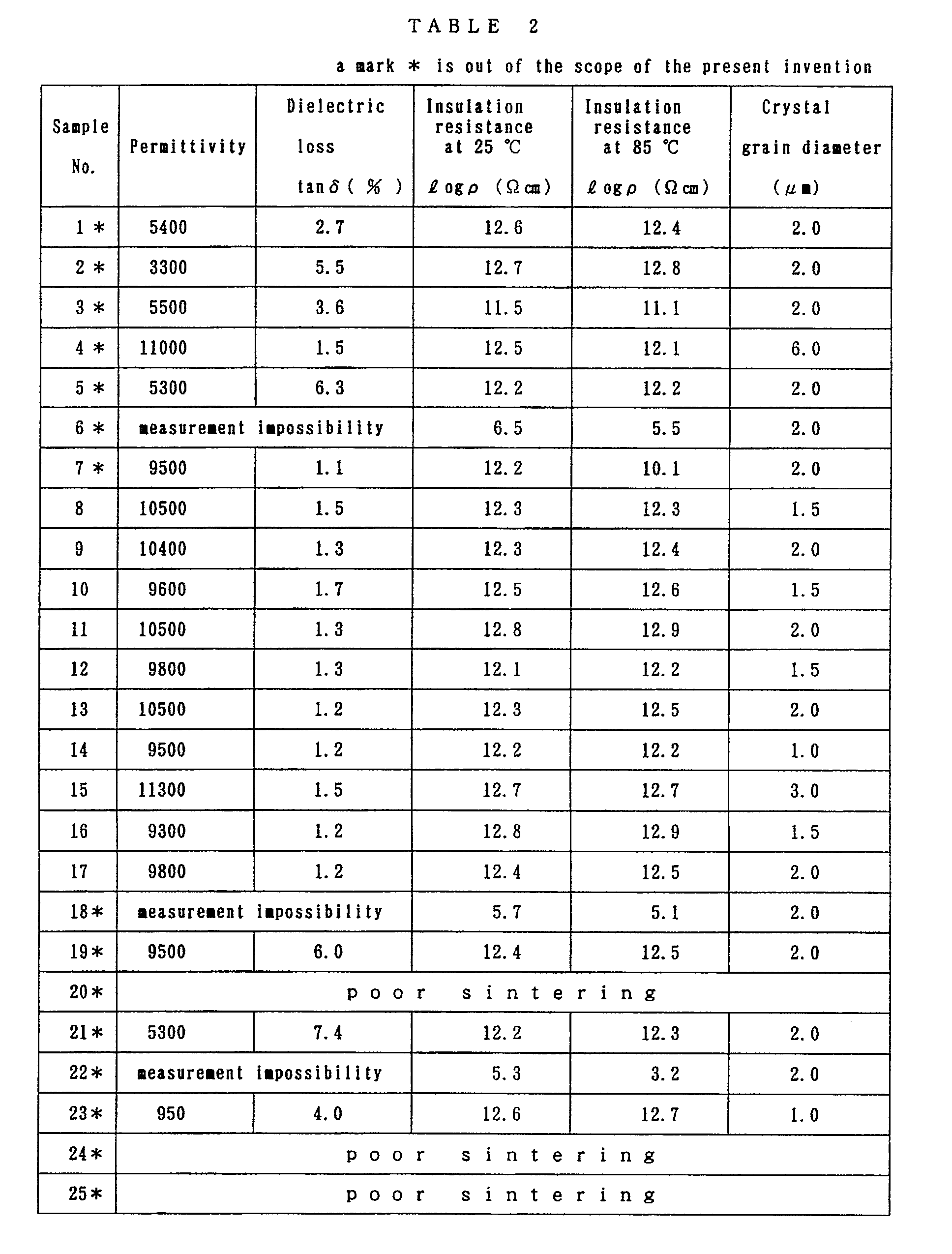
- For the resulting sample, an electrostatic capacity (c) and a dielectric loss (tan δ ) were measured at the condition of 1KHz and 1 Vrms using an automatic bridge. The insulation resistance (R) was taken a value measured by a high insulation resistance tester after applying the DC voltage of 500V for two minutes. The insulation resistance was measured at 25oC and 85oC and logarithms (log ρ ) of respective resistivities were calculated. Meanwhile, the crystal grain diameter of the sample was evaluated by observing the sample surface with an electron microscope. The measured results are shown in Table 2.
- Next, restricted reasons of respective compositions will be explained.
- In (Ba1-ℓ-m-n-oSrℓCamMgnCeo)q(Ti1-pZrp)O₃, in case the strontium quantity ℓ is 0.05 or less as the Sample No. 1, sintering of the ceramics is poor and the permittivity becomes smaller below 6000. When the strontium quantity ℓ exceeds 0.30 as the Sample No. 25, the sintering becomes extremely poor, which is not desirable.
- Furthermore, in case the calcium quantity m is less than 0.005 as the Sample No. 2, sintering of the ceramics is poor and the permittivity becomes below 6000 and the dielectric loss exceeds 5.0%. Meanwhile, when the calcium quantity m exceeds 0.22 as the Sample No. 24, the sintering becomes extremely poor, which is not desirable.
- Also, when the magnesium quantity n is less than 0.0005 as the Sample No. 3, sintering of the ceramics is poor and the permittivity becomes smaller below 6000. On the other hand, in case the magnesium quantity n exceeds 0.05 as the Sample No. 23, the permittivity becomes smaller below 1000.
- In case the cerium quantity o is less than 0.0005 as the Sample No. 4, it is not desirable because the crystal grain diameter of the ceramics exeeds 3 µm, and a dielectric layer is impossible to be formed into a thin film. On the other hand, the cerium quantity o exceeds 0.02 as the Sample 22, the ceramics fired in the reducing atmosphere is reduced and becomes semiconductive, thus the insulation resistance is lowered drastically, which is not desirable.
- In case the zirconium quantity p is 0 as the Sample 5, the dielectric loss becomes larger above 5.0%. On the other hand, when the zirconium quantity p exceeds 0.20 as the Sample 21, the sintering is poor, the permittivity becomes below 6000 and the dielectric loss becomes above 5.0%, which is not desirable.
- When a molar ratio q of (Ba1-ℓ-m-n-oSrℓCamMgnCeo) is less than 1.002 as the Sample 6, the ceramics fired in the reducing atmosphere is reduced and the insulation resistance is lowered. Meanwhile, when the molar ratio q exceeds 1.03 as the Sample No. 20, the sintering is poor, which is not desirable.
- In case the quantity of MnO₂, Fe₂O₃, Cr₂O₃ and CoO as additives is less than 0.02 mole % as the Sample 7, the insulation resistance at 85°C or more becomes smaller and reliability on the long use at high temperature is deteriorated the reliability. Meanwhile, when the quantity of additives exceeds 2.0 mole % as the Samples 18 and 19, the dielectric loss becomes 5.0% or more, which is not desirable.
- On the contrary, when the nonreducing dielectric ceramic composition of the present invention is used, the ceramics is not reduced even when fired in the reducing atmosphere, thus the dielectric ceramics with limited deterioration of insulation resistance can be obtained. Accordingly, base metals such as nickel and the like can be used as the material of the internal electrode and the cost of the monolithic ceramic capacitor can be reduced.
- Furthermore, the crystal grain diameter is small below 3 µm and a large number of crystal grains present between the dielectric layers even when the dielectric layer is formed into a thin film, so that the dielectric ceramics having a high reliability can be manufactured. In addition, since the dielectric ceramics can be formed into a thin film, the monolithic ceramic capacitor can be miniaturized.
- While the present invention has been particularly described, it is to be understood that such description is used as an example rather than limitation, and the spirit and scope of the present invention is determined solely by the terms of the appended calims.

Claims (1)
- A nonreducing dielectric ceramic composition comprising, a main component consisting of respective oxides of Ba, Ca, Mg, Sr, Ce, Ti and Zr, represented by the following formula,
(Ba1-ℓ-m-n-oSrℓCamMgnCeo)q(Ti1-pZrp)O₃
where, ℓ, m, n, o, p and q satisfying,
0.05 ≦ ℓ ≦ 0.30
0.005 ≦ m ≦ 0.22
0.0005 ≦ n ≦ 0.05
0.0005 ≦ o ≦ 0.02
0 < p ≦ 0.02
1.002 ≦ q ≦ 1.03, and
for said main component of 100 mole %, at least one of respective oxides is added by 0.02 to 2.0 mole %, when the respective oxides of Mn, Fe, Cr, Co are represented as MnO₂, Fe₂O₃, Cr₂O₃ and CoO.
Applications Claiming Priority (2)
| Application Number | Priority Date | Filing Date | Title |
|---|---|---|---|
| JP2063664A JPH0734326B2 (en) | 1990-03-13 | 1990-03-13 | Non-reducing dielectric ceramic composition |
| JP63664/90 | 1990-03-13 |
Publications (3)
| Publication Number | Publication Date |
|---|---|
| EP0446814A2 true EP0446814A2 (en) | 1991-09-18 |
| EP0446814A3 EP0446814A3 (en) | 1993-03-10 |
| EP0446814B1 EP0446814B1 (en) | 1995-10-18 |
Family
ID=13235839
Family Applications (1)
| Application Number | Title | Priority Date | Filing Date |
|---|---|---|---|
| EP19910103610 Expired - Lifetime EP0446814B1 (en) | 1990-03-13 | 1991-03-08 | Nonreducing dielectric ceramic composition |
Country Status (3)
| Country | Link |
|---|---|
| EP (1) | EP0446814B1 (en) |
| JP (1) | JPH0734326B2 (en) |
| DE (1) | DE69113838T2 (en) |
Cited By (4)
| Publication number | Priority date | Publication date | Assignee | Title |
|---|---|---|---|---|
| EP0630032A1 (en) * | 1993-06-15 | 1994-12-21 | Murata Manufacturing Co., Ltd. | Non-reducible dielectric ceramic composition |
| KR100415558B1 (en) * | 2000-03-31 | 2004-01-24 | 삼성전기주식회사 | Dielectric ceramic composition, ceramic capacitor using the composition and process of producing same |
| EP1496030A4 (en) * | 2002-04-16 | 2008-08-06 | Murata Manufacturing Co | Nonreducing dielectric ceramic, its production method, and multilayer ceramic capacitor |
| CN107056290A (en) * | 2016-11-04 | 2017-08-18 | 西安交通大学 | A kind of method of regulation and control ferroelectric ceramics Curie temperature |
Family Cites Families (3)
| Publication number | Priority date | Publication date | Assignee | Title |
|---|---|---|---|---|
| JPS60131707A (en) * | 1983-12-19 | 1985-07-13 | 株式会社村田製作所 | Nonreduced temperature compensating dielectric porcelain composition |
| JPS6119005A (en) * | 1984-07-05 | 1986-01-27 | 株式会社村田製作所 | Nonreduced dielectric porcelain composition |
| JPH0821266B2 (en) * | 1987-03-11 | 1996-03-04 | 株式会社村田製作所 | Dielectric paste |
-
1990
- 1990-03-13 JP JP2063664A patent/JPH0734326B2/en not_active Expired - Lifetime
-
1991
- 1991-03-08 DE DE1991613838 patent/DE69113838T2/en not_active Expired - Lifetime
- 1991-03-08 EP EP19910103610 patent/EP0446814B1/en not_active Expired - Lifetime
Cited By (7)
| Publication number | Priority date | Publication date | Assignee | Title |
|---|---|---|---|---|
| EP0630032A1 (en) * | 1993-06-15 | 1994-12-21 | Murata Manufacturing Co., Ltd. | Non-reducible dielectric ceramic composition |
| US5510305A (en) * | 1993-06-15 | 1996-04-23 | Murata Manufacturing Co., Ltd. | Non-reducible dielectric ceramic composition |
| KR100415558B1 (en) * | 2000-03-31 | 2004-01-24 | 삼성전기주식회사 | Dielectric ceramic composition, ceramic capacitor using the composition and process of producing same |
| EP1496030A4 (en) * | 2002-04-16 | 2008-08-06 | Murata Manufacturing Co | Nonreducing dielectric ceramic, its production method, and multilayer ceramic capacitor |
| US7498285B2 (en) | 2002-04-16 | 2009-03-03 | Murata Manufacturing Co., Ltd. | Nonreducing dielectric ceramic, and manufacturing method and monolithic ceramic capacitor of the same |
| CN107056290A (en) * | 2016-11-04 | 2017-08-18 | 西安交通大学 | A kind of method of regulation and control ferroelectric ceramics Curie temperature |
| CN107056290B (en) * | 2016-11-04 | 2021-01-19 | 西安交通大学 | Method for regulating Curie temperature of ferroelectric ceramic |
Also Published As
| Publication number | Publication date |
|---|---|
| JPH0734326B2 (en) | 1995-04-12 |
| DE69113838T2 (en) | 1996-06-20 |
| EP0446814B1 (en) | 1995-10-18 |
| JPH03263708A (en) | 1991-11-25 |
| DE69113838D1 (en) | 1995-11-23 |
| EP0446814A3 (en) | 1993-03-10 |
Similar Documents
| Publication | Publication Date | Title |
|---|---|---|
| US5668694A (en) | Multilayer ceramic chip capacitor | |
| CN100559523C (en) | Dielectric ceramic, method of manufacturing same, and monolithic ceramic capacitor | |
| EP0977218B1 (en) | Dielectric ceramic composition and electronic device | |
| EP0785561B1 (en) | Dielectric ceramic composition and its use in a monolithic ceramic capacitor | |
| KR100414331B1 (en) | Nonreducing dielectric ceramic and monolithic ceramic capacitor using the same | |
| JP3503568B2 (en) | Non-reducing dielectric ceramic and multilayer ceramic capacitor using the same | |
| JP2001006966A (en) | Ceramic capacitor and method of manufacturing the same | |
| KR980009197A (en) | Multilayer Ceramic Capacitors | |
| US7396791B2 (en) | Electronic device, dielectric ceramic composition and the production method | |
| CN113321501A (en) | Dielectric composition and laminated electronic component | |
| US5130281A (en) | Dielectric ceramic compositions and manufacturing method of dielectric ceramics | |
| EP0103338B1 (en) | Low-fire ceramic dielectric compositions | |
| JP3319273B2 (en) | Non-reducing dielectric porcelain composition | |
| JPH0831232A (en) | Non-reducing dielectric ceramic composition | |
| US5202814A (en) | Nonreducing dielectric ceramic composition | |
| EP0180132A2 (en) | High dielectric constant type ceramic composition | |
| EP0446814B1 (en) | Nonreducing dielectric ceramic composition | |
| JP2004217509A (en) | Nonreducible dielectric ceramic and multilayer ceramic capacitor | |
| JPH10139538A (en) | Dielectric porcelain composition | |
| JP2006342025A (en) | Dielectric ceramic composition and electronic component | |
| JP3450919B2 (en) | Dielectric ceramic composition for temperature compensation | |
| JP3401145B2 (en) | Dielectric porcelain composition | |
| JP3438334B2 (en) | Non-reducing dielectric porcelain composition | |
| JP3245313B2 (en) | Dielectric porcelain composition | |
| JPH04368709A (en) | Nonreducing dielectric porcelain composition material |
Legal Events
| Date | Code | Title | Description |
|---|---|---|---|
| PUAI | Public reference made under article 153(3) epc to a published international application that has entered the european phase |
Free format text: ORIGINAL CODE: 0009012 |
|
| AK | Designated contracting states |
Kind code of ref document: A2 Designated state(s): DE FR GB |
|
| PUAL | Search report despatched |
Free format text: ORIGINAL CODE: 0009013 |
|
| AK | Designated contracting states |
Kind code of ref document: A3 Designated state(s): DE FR GB |
|
| 17P | Request for examination filed |
Effective date: 19930527 |
|
| 17Q | First examination report despatched |
Effective date: 19940527 |
|
| GRAA | (expected) grant |
Free format text: ORIGINAL CODE: 0009210 |
|
| AK | Designated contracting states |
Kind code of ref document: B1 Designated state(s): DE FR GB |
|
| REF | Corresponds to: |
Ref document number: 69113838 Country of ref document: DE Date of ref document: 19951123 |
|
| ET | Fr: translation filed | ||
| PLBE | No opposition filed within time limit |
Free format text: ORIGINAL CODE: 0009261 |
|
| STAA | Information on the status of an ep patent application or granted ep patent |
Free format text: STATUS: NO OPPOSITION FILED WITHIN TIME LIMIT |
|
| 26N | No opposition filed | ||
| REG | Reference to a national code |
Ref country code: GB Ref legal event code: IF02 |
|
| PGFP | Annual fee paid to national office [announced via postgrant information from national office to epo] |
Ref country code: FR Payment date: 20100324 Year of fee payment: 20 |
|
| PGFP | Annual fee paid to national office [announced via postgrant information from national office to epo] |
Ref country code: GB Payment date: 20100303 Year of fee payment: 20 |
|
| PGFP | Annual fee paid to national office [announced via postgrant information from national office to epo] |
Ref country code: DE Payment date: 20100318 Year of fee payment: 20 |
|
| REG | Reference to a national code |
Ref country code: DE Ref legal event code: R071 Ref document number: 69113838 Country of ref document: DE |
|
| REG | Reference to a national code |
Ref country code: GB Ref legal event code: PE20 Expiry date: 20110307 |
|
| PG25 | Lapsed in a contracting state [announced via postgrant information from national office to epo] |
Ref country code: GB Free format text: LAPSE BECAUSE OF EXPIRATION OF PROTECTION Effective date: 20110307 |
|
| PG25 | Lapsed in a contracting state [announced via postgrant information from national office to epo] |
Ref country code: DE Free format text: LAPSE BECAUSE OF EXPIRATION OF PROTECTION Effective date: 20110308 |