EP0446827A1 - Terminal installation for asynchronous network - Google Patents
Terminal installation for asynchronous network Download PDFInfo
- Publication number
- EP0446827A1 EP0446827A1 EP91103673A EP91103673A EP0446827A1 EP 0446827 A1 EP0446827 A1 EP 0446827A1 EP 91103673 A EP91103673 A EP 91103673A EP 91103673 A EP91103673 A EP 91103673A EP 0446827 A1 EP0446827 A1 EP 0446827A1
- Authority
- EP
- European Patent Office
- Prior art keywords
- interface
- adapter
- circuit
- access
- optical
- Prior art date
- Legal status (The legal status is an assumption and is not a legal conclusion. Google has not performed a legal analysis and makes no representation as to the accuracy of the status listed.)
- Granted
Links
- 238000009434 installation Methods 0.000 title claims abstract description 26
- 230000003287 optical effect Effects 0.000 claims abstract description 48
- 239000011159 matrix material Substances 0.000 claims abstract description 22
- 230000002457 bidirectional effect Effects 0.000 claims abstract description 8
- 230000005540 biological transmission Effects 0.000 claims description 35
- 238000000605 extraction Methods 0.000 claims description 22
- 238000003780 insertion Methods 0.000 claims description 12
- 230000037431 insertion Effects 0.000 claims description 12
- 101100234975 Homo sapiens LCE1A gene Proteins 0.000 claims description 6
- 101100234977 Homo sapiens LCE1B gene Proteins 0.000 claims description 6
- 102100030820 Late cornified envelope protein 1A Human genes 0.000 claims description 6
- 102100030821 Late cornified envelope protein 1B Human genes 0.000 claims description 6
- 101100476608 Saccharomyces cerevisiae (strain ATCC 204508 / S288c) SAC3 gene Proteins 0.000 claims description 6
- 230000011664 signaling Effects 0.000 abstract description 15
- 238000000034 method Methods 0.000 abstract description 4
- 230000006978 adaptation Effects 0.000 description 10
- 230000006870 function Effects 0.000 description 10
- 230000033764 rhythmic process Effects 0.000 description 9
- 238000012546 transfer Methods 0.000 description 8
- 230000001360 synchronised effect Effects 0.000 description 6
- 101000896414 Homo sapiens Nuclear nucleic acid-binding protein C1D Proteins 0.000 description 5
- 101001043564 Homo sapiens Prolow-density lipoprotein receptor-related protein 1 Proteins 0.000 description 5
- 102100021923 Prolow-density lipoprotein receptor-related protein 1 Human genes 0.000 description 5
- 238000012986 modification Methods 0.000 description 5
- 230000004048 modification Effects 0.000 description 5
- 101001043562 Homo sapiens Low-density lipoprotein receptor-related protein 2 Proteins 0.000 description 4
- 102100021922 Low-density lipoprotein receptor-related protein 2 Human genes 0.000 description 4
- 238000010586 diagram Methods 0.000 description 4
- 102100026559 Filamin-B Human genes 0.000 description 3
- 101000913551 Homo sapiens Filamin-B Proteins 0.000 description 3
- 238000004891 communication Methods 0.000 description 3
- 238000012544 monitoring process Methods 0.000 description 3
- 238000001514 detection method Methods 0.000 description 2
- 238000005516 engineering process Methods 0.000 description 2
- 230000004907 flux Effects 0.000 description 2
- 230000000737 periodic effect Effects 0.000 description 2
- 238000011084 recovery Methods 0.000 description 2
- 241001415961 Gaviidae Species 0.000 description 1
- 240000008042 Zea mays Species 0.000 description 1
- 230000003466 anti-cipated effect Effects 0.000 description 1
- 238000005259 measurement Methods 0.000 description 1
- 239000003607 modifier Substances 0.000 description 1
- 239000013307 optical fiber Substances 0.000 description 1
- 238000012545 processing Methods 0.000 description 1
- 230000001172 regenerating effect Effects 0.000 description 1
- 230000008929 regeneration Effects 0.000 description 1
- 238000011069 regeneration method Methods 0.000 description 1
- 230000000717 retained effect Effects 0.000 description 1
- 230000009131 signaling function Effects 0.000 description 1
- 230000017105 transposition Effects 0.000 description 1
- 238000012795 verification Methods 0.000 description 1
Images
Classifications
-
- H—ELECTRICITY
- H04—ELECTRIC COMMUNICATION TECHNIQUE
- H04Q—SELECTING
- H04Q11/00—Selecting arrangements for multiplex systems
- H04Q11/04—Selecting arrangements for multiplex systems for time-division multiplexing
- H04Q11/0428—Integrated services digital network, i.e. systems for transmission of different types of digitised signals, e.g. speech, data, telecentral, television signals
- H04Q11/0478—Provisions for broadband connections
-
- H—ELECTRICITY
- H04—ELECTRIC COMMUNICATION TECHNIQUE
- H04L—TRANSMISSION OF DIGITAL INFORMATION, e.g. TELEGRAPHIC COMMUNICATION
- H04L12/00—Data switching networks
- H04L12/54—Store-and-forward switching systems
- H04L12/56—Packet switching systems
- H04L12/5601—Transfer mode dependent, e.g. ATM
- H04L2012/5614—User Network Interface
-
- Y—GENERAL TAGGING OF NEW TECHNOLOGICAL DEVELOPMENTS; GENERAL TAGGING OF CROSS-SECTIONAL TECHNOLOGIES SPANNING OVER SEVERAL SECTIONS OF THE IPC; TECHNICAL SUBJECTS COVERED BY FORMER USPC CROSS-REFERENCE ART COLLECTIONS [XRACs] AND DIGESTS
- Y10—TECHNICAL SUBJECTS COVERED BY FORMER USPC
- Y10S—TECHNICAL SUBJECTS COVERED BY FORMER USPC CROSS-REFERENCE ART COLLECTIONS [XRACs] AND DIGESTS
- Y10S370/00—Multiplex communications
- Y10S370/901—Wide area network
- Y10S370/902—Packet switching
- Y10S370/903—Osi compliant network
- Y10S370/907—Synchronous optical network, SONET
Definitions
- the invention relates to a subscriber terminal installation.
- a subscriber terminal installation generally makes it possible to interconnect terminals of a user, and to connect these terminals to a public network.
- the subscriber terminal installations have so far been most often constructed on the basis of a synchronous transfer mode in which the information to be exchanged occupies a fixed speed channel, 64 kbit / s for example.
- the synchronous transfer mode is used in digital networks incorporating narrowband services, ISDN-BE.
- the asynchronous transfer mode, MTA is anticipated for the implementation of networks with integrated broadband services, BISDN, allowing, in addition to the continuity of ISDN-BE services, the advent of new services requiring bit rates at values higher and multiple.
- This asynchronous transfer mode has the particularity of being able to route any bit rate, provided that it remains below the maximum bit rate of the conduit used for transmission.
- the information is transported in the form of cells of fixed length. These cells include a fixed length header and an information field also of fixed length. The information belonging to a particular communication is identified by a virtual circuit number contained in the header of the cell.
- This mode of information multiplexing allows the routing of arbitrary bit rates without any other transmission frame structure than that of the cell.
- the header has a length of 4 bytes and that the information field has a length of 32 bytes, that is to say a total of 36 bytes in length for a cell; of course the header and the information field can have different lengths from those indicated above.
- the object of the invention is to provide a subscriber installation, based on the asynchronous transfer mode, allowing on the one hand the continuity of the services offered by connected synchronous terminals to an existing installation, and on the other hand, an opening towards new services at speeds still not fully identified.
- Another object of the invention is to provide a subscriber terminal installation which can evolve in order to adapt to the needs of the user.
- the present invention relates to the digital TNA subscriber termination and the means of connecting said termination to the digital termination of the TNR network and to the terminals.
- One of the essential characteristics of such a subscriber terminal installation is that the actual speed at the Sb and Tb interfaces is possible at multiple speeds without modification of the other functionalities, according to the real needs of the installation.
- FIG. 3 represents the diagram of a digital broadband subscriber termination TNA.LB of FIG. 2.
- the TNA.LB termination comprises a switching matrix MC, two access groups G1 and G2, and an AL supply.
- Each access group comprises four access modules MA each connected by a control link LC to a processor PR which plays the role of local controller; the power supply AL is connected to the switching matrix MC and to the access groups.
- the ports P1 to P8 of the termination are each connected to an access module.
- the switching matrix MC of a type known per se, is, in this example, of the type with 8 inputs and 8 outputs; each access module MA is therefore connected to an input and to an output of the switching matrix MC.
- the processor PR performs the signaling processing and supervision functions of the four access modules MA of the access group.
- the ports P1 to P7 are each connected to an optical interface, Sb, the port P8 being connected to the optical interface Tb, as shown in FIG. 2.
- FIG. 4 represents the diagram of an access module MA of the access groups G1 and G2 in Figure 3.
- the online throughput of the optical interfaces can be arbitrary, but to take account of implementation problems, only a few throughput values are retained, for example: 600 Mbit / s for the Tb interface and the Sb interfaces with the fastest terminals (high definition images for example), 150 Mbit / s, this speed covering a wide range of services at intermediate speeds, and 10 Mbit / s, this speed being directly accessible to all technologies and can be used for band services narrow.
- the MA access modules therefore all have the same structure and differ only in the frequency of a local clock signal, this frequency being 600 MHz, 150 MHz, or 10 MHz.
- the Pi port is connected to an optical duplexer 1, itself connected to an optical transmitter 2 and to an optical receiver 3.
- the optical transmitter comprises a laser at 1550 nm
- the optical receiver comprises a PIN diode.
- a clock module 4 ensures the generation of a local clock signal HL, at the data rate for the transmission direction (600, 150, or 10 Mbit / s), and the recovery of rhythm from the data for the reception direction, the clock module being connected a serial reception link LRS1 at the output of the optical receiver 3.
- a regenerator 5, for regenerating in level and in time the data received, is connected to the optical receiver by the serial reception link LRS1 and clock module 4 which delivers a recovered clock signal HR to it.
- a parallel-series circuit 6, scrambler is connected to the optical transmitter 2 by a series transmission link LES, and to the regenerator 5 by a series reception link LRS2; it also receives from the clock module the local clock signal HL and the recovered clock signal HR.
- a cell extraction insertion circuit 7, for the insertion and extraction of signaling cells, is connected to the parallel-serial scrambler circuit 6 by a parallel transmit link LEP2 and a parallel receive link LRP1, for delivering data to the parallel-series circuit 6 (transmission direction) and to receive it (reception direction); it is also connected by a bidirectional control link LC to the processor PR of the group to which the access module belongs and to the clock module 4 from which it receives the local clock signal HL.
- An interface circuit 8 is connected to the extractor insertion circuit 7 by a parallel transmission link LEP1 and by a parallel reception link LRP2; it is also connected to the switching matrix MC by a transmission line LE and a reception line LR.
- the interface circuit 8 carries out the transposition between the transmission line LE and the parallel transmission link LEP1, and between the parallel reception link LRP2 and the reception line LR.
- the LE transmission and LR reception links are either of the parallel type, with four 150 Mbit / s data wires, one wire for a 150 MHz clock signal and one wire for a 150 MHz signal.
- cell start ie with a single wire for a serial bit rate at 600 Mbit / s with signal regeneration and rhythm recovery.
- the parallel transmit LEP1 and LEP2, and parallel receive LRP1 and LRP2 links are each with eleven wires: eight data wires, FD1 ... 8 (one for each bit of a byte), one F9 wire for one clock signal byte HO at link speed, one wire F10 for one signal full cell PC, at level 0 for the entire duration of a full cell, and a wire F11 for a signal beginning cell SDC, at level 0 at the beginning of a cell, that is to say at the first byte d 'a full cell.
- the optical receiver 3 comprises, in addition to the PIN diode, a preamplifier and an amplifier with automatic gain control, as is well known to those skilled in the art; the regenerator 5 can also be part of the optical receiver.
- FIG. 5 represents the clock module 4 of FIG. 4; this module includes an oscillator 10 and a rhythm recuperator 11.
- the oscillator delivers the local clock signal HL, the frequency of which is 600, or 150, or 10 MHz.
- the rhythm recuperator 11 is connected at the input, by the serial reception link LRS1, to the optical receiver 3, and delivers the recovered clock signal HR.
- FIG. 6 represents the scrambler parallel-series circuit 6 of FIG. 4, which comprises a transmission channel and a reception channel.
- the transmission channel is constituted by a cell parity calculation circuit 15, connected at input to the parallel transmission link LEP2, a serialization circuit 16 connected by a link 17 at output of circuit 15 and receiving the signal local clock HL and a send byte clock signal HOE by the link LEP2, and a scrambling circuit 18 the input of which is connected at the output of the circuit 16 by a serial link 19, and the output is linked to the serial transmission link LES, said circuit 18 also being connected to wire F11 of the link LEP2, from which it receives the start signal of the SDC cell.
- the reception channel is constituted by a synchronization device 30, for the search and verification of synchronization, connected at the input to the LRS2 serial reception link, a descrambling circuit 31 connected by a link 31a at the output of the synchronization device 30 , a paralleling circuit 32 connected by a link 31b at the output of the descrambling circuit 31, and a parity checking circuit 33 connected at the output of the paralleling circuit 32 by a parallel link 29 and having its output connected to the eight data wires F1 ... 8 from the parallel reception link LRP1.
- the synchronization 30 is connected to the full cell wires F10 and cell start F11, of the parallel reception link LRP1 to which it delivers the full cell PC and cell start SPC signals, respectively.
- the descrambling circuit 31 is also connected to the cell start wire F11.
- the paralleling circuit 32 receives the recovered clock signal HR and a recovered byte clock signal HOR delivered by a divider by eight 34 from the signal HR; the output of the divider is also connected to wire F9 of the LRP1 link.
- the synchronization device 30 is of any known type and in particular of the type described in published European application 0301934, entitled: Time switching system for packets of different lengths.
- the scrambling or descrambling is carried out by a device represented in FIG. 7, and constituted by a positioning circuit 50, a pseudo-random sequence generator 51, and an adder 52.
- the generator is synchronized at the start of each cell; for this, the positioning circuit 50 receives the cell start signal SDC, and delivers a positioning signal to the generator which takes the state 1111111, at the start of each cell; the generator has its output looped back to its input, and connected to an input of the adder 52, another input of which is connected to a link 53 by which it receives information; the output of the adder is connected to a link 54.
- the links 53 and 54 are respectively the serial link 19 and the transmission link in series LES; when the device is used as a descrambler circuit 31, FIG. 6, the links 53 and 54 are respectively the links 31a and 31b.
- the descrambling of the information is also carried out by adding to the scrambled information a pseudo-random sequence delivered by the generator 51 of the circuit 31 and synchronized by the start signal of the SDC cell. This addition is carried out under the same conditions as those of scrambling.
- the parity check circuit 33 checks the parity of the logical number of 1 of the entire contents of the cell (header and information field). The parity having been forced on transmission, the detection of an imparity allows the detection of a transmission error. The result of this parity calculation is transmitted to the cell insertion-extraction circuit 7 for accounting.
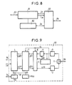
- FIG. 8 represents the general diagram of an AT.LB or AT.BE terminal adapter of FIG. 2, constituted by a multiplex adapter 60, a service adapter 61, and a control circuit 62 for controlling the service adapter 61.
- the multiplex adapter 60 is connected on the one hand to the interface Sb which is an asynchronous optical interface carrying an asynchronous multiplex, and on the other hand to the service adapter 61 by a downlink interface Id and a uplink interface Im; the adapter 60 is also connected to the control circuit 62 by a control interface Ic.
- the service adapter is also connected via an interface 63 to a broadband terminal TE.LB or to a narrowband termination TNA.BE, depending on whether the terminal adapter is broadband, AT.LB, or narrowband AT.BE.
- the interfaces Id and Im allow the exchange of information organized in cells, and the interface Ic allows the exchange of command or signaling messages.
- the downward interface Id routes a downstream flow of data organized in cells in the direction of multiplex adapter 60 to service adapter 61; it consists of eight data wires organized in bytes, a byte clock wire, and a cell synchronization wire.
- the uplink interface Im routes a data flow organized in cells in the direction of service adapter 61 to the multiplex adapter 60; like the downlink interface Id, it is made up of eight data wires organized in bytes, a byte clock wire, and a cell synchronization wire.
- the control interface Ic routes the control and signaling information exchanged, in both directions, between the control circuit 62 and the multiplex adapter 60; it consists of a single physical medium allowing the bus connection of several user terminations.
- FIG. 9 represents the multiplex adapter 60 of FIG. 9.
- This multiplex adapter constitutes the common part of the terminal adapters AT.LB and AT.BE, and provides functions independent of the services: adaptations to the interfaces Sb, Id and Im, and insertion-extraction of signaling.
- the multiplex adapter has a structure largely inspired by that of the access module, represented in FIG.
- the multiplex adapter comprises a PRA processor connected by a link 58 to the interface I and to the cell insertion-extraction circuit 7, and a control interface circuit 59 connected to the interface Ic and to the link. 58.
- the PRA processor and the interface circuit 59 constitute a control part of the adapter, for the signaling functions.
- the service adapter 61 in FIG. 8 performs the specific function of a service; there is therefore a specific adapter per service.
- a service adapter In the transmission direction (upward direction) a service adapter performs the functions of celling information and terminating signaling.
- an adapter performs the functions of retrieving the information transported in cells, retrieving the service rhythm, and signaling termination.
Landscapes
- Engineering & Computer Science (AREA)
- Computer Networks & Wireless Communication (AREA)
- Data Exchanges In Wide-Area Networks (AREA)
- Optical Communication System (AREA)
- Communication Control (AREA)
- Exchange Systems With Centralized Control (AREA)
- Use Of Switch Circuits For Exchanges And Methods Of Control Of Multiplex Exchanges (AREA)
Abstract
Installation terminale d'abonnée pour réseau asynchrone, ayant une terminaison numérique d'abonné (TNA) comprenant une matrice de commutation (MC) et des modules d'accès (MA) reliés chacun d'une part à la matrice de commutation et d'autre part à une interface optique asynchrone ; l'un des modules d'accès est relié à une terminaison numérique de réseau (TNR) les autres modules d'accès étant reliés chacun soit à un terminal soit à un adaptateur de terminal. Un processeur (PR) relié aux modules traite la signalisation reçue ou à émettre par les modules d'accès. Un adaptateur de terminal comprend un adaptateur de multiplex, un adaptateur de service, spécifique d'un service, et un circuit de commande : l'adaptateur de multiplex est relié par une interface optique asynchrone bidirectionnelle à un module d'accès et par une interface montante et une interface descendante à l'adaptateur de service, lesdites interfaces montantes et descendantes étant des interfaces asynchrones acheminant des cellules.
Description
L'invention concerne une installation terminale d'abonné. Une installation terminale d'abonné permet, d'une manière générale d'interconnecter entre eux des terminaux d'un usager, et de relier ces terminaux à un réseau public.The invention relates to a subscriber terminal installation. A subscriber terminal installation generally makes it possible to interconnect terminals of a user, and to connect these terminals to a public network.
Les installations terminales d'abonnés ont été, jusqu'à présent, le plus souvent construites sur la base d'un mode de transfert synchrone dans lequel l'information à échanger occupe un canal de débit fixe, 64 kbit/s par exemple. Le mode de transfert synchrone est utilisé dans les réseaux numériques à intégration de services à bande étroite, RNIS-BE.The subscriber terminal installations have so far been most often constructed on the basis of a synchronous transfer mode in which the information to be exchanged occupies a fixed speed channel, 64 kbit / s for example. The synchronous transfer mode is used in digital networks incorporating narrowband services, ISDN-BE.
Le mode de transfert asynchrone, MTA, est pressenti pour la mise en oeuvre des réseaux à intégration de services large bande, BISDN, permettant, outre le continuité des services du RNIS-BE, l'avènement de nouveaux services nécessitant des débits à des valeurs plus élevées et multiples. Ce mode de transfert asynchrone présente la particularité de pouvoir acheminer n'importe quel débit, pourvu qu'il reste inférieur au débit maximal du conduit utilisé pour la transmission.The asynchronous transfer mode, MTA, is anticipated for the implementation of networks with integrated broadband services, BISDN, allowing, in addition to the continuity of ISDN-BE services, the advent of new services requiring bit rates at values higher and multiple. This asynchronous transfer mode has the particularity of being able to route any bit rate, provided that it remains below the maximum bit rate of the conduit used for transmission.
Dans le mode de transfert asynchrone l'information est transportée sous la forme de cellules de longueur fixe. Ces cellules comprennent un en-tête de longueur fixe et un champ d'information également de longueur fixe. L'information appartenant à une communication particulière est identifiée grâce à un numéro de circuit virtuel contenu dans l'en-tête de la cellule. Ce mode de multiplexage de l'information permet l'acheminement de débits quelconques sans autre structure de trame de transmission que celle de la cellule. Dans tout ce qui suit on a supposé, uniquement à titre d'exemple, que l'en-tête avait une longueur de 4 octets et que le champ d'information avait une longueur de 32 octets, soit au total 36 octets de longueur pour une cellule; bien entendu l'en-tête et le champ d'information peuvent avoir des longueurs différentes de celles indiquées ci-dessus.In the asynchronous transfer mode the information is transported in the form of cells of fixed length. These cells include a fixed length header and an information field also of fixed length. The information belonging to a particular communication is identified by a virtual circuit number contained in the header of the cell. This mode of information multiplexing allows the routing of arbitrary bit rates without any other transmission frame structure than that of the cell. In what follows, it has been assumed, by way of example only, that the header has a length of 4 bytes and that the information field has a length of 32 bytes, that is to say a total of 36 bytes in length for a cell; of course the header and the information field can have different lengths from those indicated above.
Le but de l'invention est de réaliser une installation d'abonné, basée sur le mode de transfert asynchrone, permettant d'une part la continuité des services offerts par des terminaux synchrones raccordés à une installation existante, et d'autre part une ouverture vers de nouveaux services à des débits encore incomplètement identifiés.The object of the invention is to provide a subscriber installation, based on the asynchronous transfer mode, allowing on the one hand the continuity of the services offered by connected synchronous terminals to an existing installation, and on the other hand, an opening towards new services at speeds still not fully identified.
Un autre but de l'invention est de réaliser une installation terminale d'abonné qui puisse évoluer afin de s'adapter aux besoins de l'usager.Another object of the invention is to provide a subscriber terminal installation which can evolve in order to adapt to the needs of the user.
L'invention a pour objet une installation terminale d'abonné pour réseau asynchrone dans lequel les informations sont organisées en cellules, comportant :
- une terminaison numérique de réseau reliée au réseau asynchrone;
- une terminaison numérique d'abonné reliée par une interface optique asynchrone bidirectionnelle à la terminaison de réseau;
- des terminaux reliés directement à ladite terminaison numérique d'abonné;
- et des terminaux reliés chacun à ladite terminaison numérique d'abonné par un adaptateur de terminal;
caractérisé par le fait que la terminaison numérique d'abonné comprend :
- une matrice de commutation;
- une pluralité de modules d'accès ayant la même structure mais fonctionnant éventuellement à des fréquences d'horloge différentes; tous les modules d'accès étant reliés à la matrice de commutation; l'un des modules d'accès étant relié en outre à la terminaison numérique de réseau par l'interface optique asynchrone bidirectionnelle, les autres modules d'accès étant reliés en outre chacun à un terminal ou à un adaptateur de terminal, par une interface optique asynchrone bidirectionnelle;
- au moins un processeur relié aux modules d'accès.
- a digital network termination connected to the asynchronous network;
- a digital subscriber termination connected by a bidirectional asynchronous optical interface to the network termination;
- terminals connected directly to said digital subscriber termination;
- and terminals each connected to said digital subscriber termination by a terminal adapter;
characterized in that the digital subscriber termination includes:
- a switching matrix;
- a plurality of access modules having the same structure but possibly operating at different clock frequencies; all the access modules being connected to the switching matrix; one of the access modules being further connected to the digital network termination by the bidirectional asynchronous optical interface, the other access modules being each further connected to a terminal or to a terminal adapter, by an interface bidirectional asynchronous optics;
- at least one processor connected to the access modules.
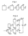
La configuration des installations d'abonné et des interfaces entre les sous ensembles des installations, telle que recommandée par le CCITT, est représentée figure 1 ; dans cette figure :
- T
- est un terminal,
- AT
- est un adaptateur de terminal,
- TNA
- est une terminaison numérique d'abonné,
- TNR
- est une terminaison numérique de réseau (terminal de réseau),
- R, S, T, U,
- sont des interfaces.
- T
- is a terminal,
- AT
- is a terminal adapter,
- TNA
- is a digital subscriber termination,
- TNR
- is a digital network termination (network terminal),
- R, S, T, U,
- are interfaces.
La présente invention concerne la terminaison numérique d'abonné TNA et les moyens de raccorder ladite terminaison à la terminaison numérique de réseau TNR et aux terminaux.The present invention relates to the digital TNA subscriber termination and the means of connecting said termination to the digital termination of the TNR network and to the terminals.
L'invention va être décrite à l'aide d'exemples non limitatifs de réalisation, illustrés par les figures annexées dans lesquelles :
- la figure 2 représente l'architecture générale d'une installation terminale d'abonné mettant en oeuvre une terminaison numérique d'abonné large bande et les moyens de raccordement de l'invention,
- la figure 3 est un schéma général de la terminaison numérique d'abonné large bande de la figure 2,
- la figure 4 représente un module d'accès de la terminaison numérique d'abonné large bande de la figure 2,
- la figure 5 représente un module horloge d'un module d'accès,
- la figure 6 représente un circuit parallèle-série embrouilleur d'un module d'accès,
- la figure 7 est un circuit utilisé en embrouilleur et en désembrouilleur dans le circuit parallèle-série embrouilleur,
- la figure 8 représente un adaptateur de terminal d'une installation terminale d'abonné, et
- la figure 9 représente un adaptateur de multiplex d'un adaptateur de terminal.
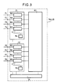
- FIG. 2 represents the general architecture of a subscriber terminal installation implementing digital broadband subscriber termination and the connection means of the invention,
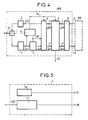
- FIG. 3 is a general diagram of the digital broadband subscriber termination of FIG. 2,
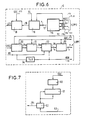
- FIG. 4 represents an access module for the digital broadband subscriber termination of FIG. 2,
- FIG. 5 represents a clock module of an access module,
- FIG. 6 represents a parallel-series scrambling circuit of an access module,
- FIG. 7 is a circuit used in scrambler and in descrambler in the parallel-series scrambler circuit,
- FIG. 8 represents a terminal adapter of a subscriber terminal installation, and
- Figure 9 shows a multiplex adapter of a terminal adapter.
La figure 2 représente l'architecture générale d'une installation terminale d'abonné comportant une terminaison numérique d'abonné large bande TNA.LB, et ses moyens de raccordement, de l'invention. Ces moyens de raccordement sont les interfaces optiques asynchrones Tb, Sb et les adaptateurs de terminaux AT.LB et AT.BE.
- L'interface optique Tb achemine un débit qui peut atteindre 600 Mbit/s ; comme dans la figure 1, cette interface Tb relie un port, P8, de la terminaison TNA.LB à la terminaison numérique de réseau TNR.
- La terminaison numérique d'abonné large bande TNA.LB assure une fonction de commutation afin d'offrir des communications locales entre les terminaux raccordés aux ports P1 à P7 de ladite terminaison par l'intermédiaire d'interfaces Sb ; ces interfaces sont au nombre de sept dans l'exemple considéré ; bien entendu le nombre d'interfaces Sb peut être différent.
- Les interfaces optiques Sb acheminent des débits qui peuvent atteindre 600 Mbit/s.
- Les terminaux large bande, TE, en mode transfert asynchrone (un seul est représenté) sont raccordés directement par une interface Sb, à un port de la terminaison TNA.LB.
- Les terminaux large bande TE.LB, à interface R non compatible avec le mode de transfert asynchrone (un seul terminal TE.LB est représenté), sont raccordés chacun par l'intermédiaire d'un adaptateur large bande AT.LB et une interface Sb, à un port de la terminaison TNA.LB.
- Les terminaux bande étroite sont supposés raccordés par une interface SO à une terminaison bande étroite TNA.BE, préalablement existante, et présentant une interface TO, (ou T2) ; cette terminaison bande étroite TNA.BE est raccordée, par l'intermédiaire d'un adaptateur bande étroite AT.BE et d'une interface optique Sb, à un port de la terminaison TNA.LB.
- The optical interface Tb carries a speed which can reach 600 Mbit / s; as in figure 1, this Tb interface connects a port, P8, from the TNA.LB termination to the digital TNR network termination.
- The digital broadband subscriber termination TNA.LB provides a switching function in order to offer local communications between the terminals connected to the ports P1 to P7 of said termination via interfaces Sb; there are seven of these interfaces in the example considered; of course the number of interfaces Sb can be different.
- The optical interfaces Sb carry speeds which can reach 600 Mbit / s.
- Broadband terminals, TE, in asynchronous transfer mode (only one is shown) are connected directly by an interface Sb, to a port of the TNA.LB termination.
- TE.LB broadband terminals, with R interface not compatible with asynchronous transfer mode (only one TE.LB terminal is shown), are each connected via an AT.LB broadband adapter and an Sb interface , to a port of the TNA.LB termination.
- The narrowband terminals are assumed to be connected by an interface SO to a narrowband termination TNA.BE, previously existing, and having an interface TO, (or T2); this TNA.BE narrowband termination is connected, via an AT.BE narrowband adapter and an Sb optical interface, to a port of the TNA.LB termination.
L'une des caractéristiques essentielles d'une telle installation terminale d'abonné est que le débit réel aux interfaces Sb et Tb est possible à de multiples débits sans modification des autres fonctionnalités, suivant les besoins réels de l'installation.One of the essential characteristics of such a subscriber terminal installation is that the actual speed at the Sb and Tb interfaces is possible at multiple speeds without modification of the other functionalities, according to the real needs of the installation.
La figure 3 représente le schéma d'une terminaison numérique d'abonné large bande TNA.LB de la figure 2.FIG. 3 represents the diagram of a digital broadband subscriber termination TNA.LB of FIG. 2.
La terminaison TNA.LB comprend une matrice de commutation MC, deux groupes d'accès G1 et G2, et une alimentation AL. Chaque groupe d'accès comporte quatre modules d'accès MA reliés chacun par une liaison de contrôle LC à un processeur PR qui joue le rôle de contrôleur local ; l'alimentation AL est reliée à la matrice de commutation MC et aux groupes d'accès. Les ports P1 à P8 de la terminaison sont reliés chacun à un module d'accès. La matrice de commutation MC, de type connu en soi, est, dans cet exemple, du type à 8 entrées et 8 sorties ; chaque module d'accès MA est donc relié à une entrée et à une sortie de la matrice de commutation MC.The TNA.LB termination comprises a switching matrix MC, two access groups G1 and G2, and an AL supply. Each access group comprises four access modules MA each connected by a control link LC to a processor PR which plays the role of local controller; the power supply AL is connected to the switching matrix MC and to the access groups. The ports P1 to P8 of the termination are each connected to an access module. The switching matrix MC, of a type known per se, is, in this example, of the type with 8 inputs and 8 outputs; each access module MA is therefore connected to an input and to an output of the switching matrix MC.
Dans chaque groupe d'accès, le processeur PR assure les fonctions de traitement de signalisation et supervision des quatre modules d'accès MA du groupe d'accès.In each access group, the processor PR performs the signaling processing and supervision functions of the four access modules MA of the access group.
Les ports P1 à P7 sont reliés chacun à une interface optique, Sb, le port P8 étant relié à l'interface optique Tb, comme représenté figure 2.The ports P1 to P7 are each connected to an optical interface, Sb, the port P8 being connected to the optical interface Tb, as shown in FIG. 2.
La figure 4 représente le schéma d'un module d'accès MA des groupes d'accès G1 et G2 de la figure 3.FIG. 4 represents the diagram of an access module MA of the access groups G1 and G2 in Figure 3.
Le port Pi du module d'accès est relié à une interface optique, Sb ou Tb. Les interfaces optiques Sb ou Tb ont comme support une fibre optique monomode, pour les deux sens de transmission, les longueurs d'ondes utilisées étant 1300 nm à la réception et 1500 nm à l'émission ; le débit dans chaque sens est inférieur ou égal à 600 Mbit/s, le signal étant un multiplex de cellules asynchrones, le code utilisé étant le code NRZ embrouillé. Aucune structure périodique n'apparaît au niveau des caractéristiques électriques du signal transporté. En particulier :
- la synchronisation cellule est assurée par la reconnaissance des cellules vides,
- les fonctions liées à l'exploitation des interfaces Sb et Tb mettent en oeuvre des cellules spécifiques à récurrence non nécessairement périodique, c'est-à-dire que le nombre exact de cellules de données ou de cellules vides qui séparent deux cellules d'exploitation de la ligne n'est pas obligatoirement constant. Ceci permet un débit en ligne qui pourrait être quelconque, sans modifier les autres caractéristiques de la ligne.
- cell synchronization is ensured by the recognition of empty cells,
- the functions linked to the operation of the interfaces Sb and Tb use specific cells with recurrence that are not necessarily periodic, that is to say that the exact number of data cells or empty cells which separate two operating cells of the line is not necessarily constant. This allows an online speed which could be arbitrary, without modifying the other characteristics of the line.
Le débit en ligne des interfaces optiques peut être quelconque, mais pour tenir compte des problèmes de réalisation, seules quelques valeurs de débit sont retenues, par exemple : 600 Mbit/s pour l'interface Tb et les interfaces Sb avec les terminaux les plus rapides (images à haute définition par exemple), 150 Mbit/s, ce débit couvrant une large gamme de services à des débits intermédiaires, et 10 Mbit/s, ce débit étant accessible directement à toutes les technologies et pouvant être utilisé pour les services bande étroite. Les modules d'accès MA ont donc tous même structure et se différencient uniquement par la fréquence d'un signal d'horloge locale, cette fréquence étant 600 MHz, 150 MHz, ou 10 MHz.The online throughput of the optical interfaces can be arbitrary, but to take account of implementation problems, only a few throughput values are retained, for example: 600 Mbit / s for the Tb interface and the Sb interfaces with the fastest terminals (high definition images for example), 150 Mbit / s, this speed covering a wide range of services at intermediate speeds, and 10 Mbit / s, this speed being directly accessible to all technologies and can be used for band services narrow. The MA access modules therefore all have the same structure and differ only in the frequency of a local clock signal, this frequency being 600 MHz, 150 MHz, or 10 MHz.
Le port Pi est relié à un duplexeur optique 1, lui-même relié à un émetteur optique 2 et à un récepteur optique 3. L'émetteur optique comporte un laser à 1550 nm, et le récepteur optique comporte une diode PIN. Un module horloge 4 assure la génération d'un signal d'horloge locale HL, au débit des données pour le sens émission (600, 150, ou 10 Mbit/s), et la récupération de rythme à partir des données pour le sens réception, le module horloge étant relié une liaison de réception série LRS1 en sortie du récepteur optique 3. Un régénérateur 5, pour régénérer en niveau et en temps les données reçues, est relié au récepteur optique par la liaison de réception série LRS1 et module horloge 4 qui lui délivre un signal d'horloge récupéré HR. Un circuit parallèle-série 6, embrouilleur, est relié à l'émetteur optique 2 par une liaison d'émission série LES, et au régénérateur 5 par une liaison de réception série LRS2 ; il reçoit également du module horloge le signal d'horloge locale HL et le signal d'horloge récupéré HR. Un circuit insertion extraction de cellules 7, pour l'insertion et l'extraction de cellules de signalisation, est relié au circuit parallèle-série embrouilleur 6 par une liaison d'émission parallèle LEP2 et une liaison de réception parallèle LRP1, pour délivrer des données au circuit parallèle-série 6 (sens émission) et en recevoir (sens réception) ; il est également relié par une liaison de contrôle LC, bidirectionnelle, au processeur PR du groupe auquel appartient le module d'accès et au module horloge 4 duquel il reçoit le signal d'horloge locale HL. Un circuit interface 8 est relié au circuit d'insertion extracteur 7 par une liaison d'émission parallèle LEP1 et par une liaison de réception parallèle LRP2 ; il est également relié à la matrice de commutation MC par une ligne d'émission LE et une ligne de réception LR.The Pi port is connected to an
Le circuit interface 8 réalise la transposition entre la ligne d'émission LE et la liaison d'émission parallèle LEP1, et entre la liaison de réception parallèle LRP2 et la ligne de réception LR. Selon la technologie utilisée, les liées d'émission LE et de réception LR sont soit du type parallèle, à quatre fils de données à 150 Mbit/s, un fil pour un signal d'horloge à 150 MHz et un fil pour un signal de début de cellule, soit à un seul fil pour un débit série à 600 Mbit/s avec régénération des signaux et récupération de rythme.The
Les liaisons d'émission parallèle LEP1 et LEP2, et de réception parallèle LRP1 et LRP2, sont à onze fils chacune : huit fils de données, FD1...8 (un pour chaque bit d'un octet), un fil F9 pour un signal d'horloge octet HO au débit de la liaison, un fil F10 pour un signal cellule pleine PC, au niveau 0 pendant toute la durée d'une cellule pleine, et un fil F11 pour un signal début cellule SDC, au niveau 0 au début d'une celulle, c'est-à-dire au premier octet d'une cellule pleine.The parallel transmit LEP1 and LEP2, and parallel receive LRP1 and LRP2 links are each with eleven wires: eight data wires, FD1 ... 8 (one for each bit of a byte), one F9 wire for one clock signal byte HO at link speed, one wire F10 for one signal full cell PC, at level 0 for the entire duration of a full cell, and a wire F11 for a signal beginning cell SDC, at level 0 at the beginning of a cell, that is to say at the first byte d 'a full cell.
Le récepteur optique 3, comporte, outre la diode PIN, un préamplificateur et un amplificateur à contrôle automatique de gain, comme cela est bien connu de l'homme de l'art ; le régénérateur 5 peut également faire partie du récepteur optique.The
La figure 5 représente le module horloge 4 de la figure 4 ; ce module comprend un oscillateur 10 et un récupérateur de rythme 11. L'oscillateur délivre le signal d'horloge locale HL, dont la fréquence est de 600, ou 150, ou 10 MHz. Le récupérateur de rythme 11 est relié en entrée, par la liaison de réception série LRS1, au récepteur optique 3, et délivre le signal d'horloge récupéré HR.FIG. 5 represents the clock module 4 of FIG. 4; this module includes an oscillator 10 and a
La figure 6 représente le circuit parallèle-série embrouilleur 6 de la figure 4, qui comprend une voie émission et une voie réception. La voie émission est constituée par un circuit de calcul de parité cellule 15, relié en entrée à la liaison d'émission parallèle LEP2, un circuit de mise en série 16 relié par une liaison 17 en sortie du circuit 15 et recevant le signal d'horloge locale HL et un signal d'horloge octet émission HOE par la liaison LEP2, et un circuit d'embrouillage 18 dont l'entrée est reliée en sortie du circuit 16 par une liaison série 19, et la sortie est reliée à liaison émission série LES, ledit circuit 18 étant également relié au fil F11 de la liaison LEP2, duquel il reçoit le signal début de cellule SDC.FIG. 6 represents the scrambler parallel-
La voie réception est constituée par un dispositif de synchronisation 30, pour la recherche et la vérification de la synchronisation, relié en entrée à la liaison de réception série LRS2, un circuit de désembrouillage 31 relié par une liaison 31a en sortie du dispositif de synchronisation 30, un circuit de mise en parallèle 32 relié par une liaison 31b en sortie du circuit de désembrouillage 31, et un circuit de vérification de parité 33 relié en sortie du circuit de mise en parallèle 32 par une liaison parallèle 29 et ayant sa sortie reliée aux huit fils de données F1...8 de la liaison de réception parallèle LRP1. D'autre part le dispositif de synchronisation 30 est relié aux fils cellule pleine F10 et début de cellule F11, de la liaison de réception parallèle LRP1 auxquels il délivre les signaux cellule pleine PC et début de cellule SPC, respectivement. Le circuit de désembrouillage 31 est également relié au fil début de cellule F11. Le circuit de mise en parallèle 32 reçoit le signal d'horloge récupéré HR et un signal d'horloge octet récupéré HOR délivré par un diviseur par huit 34 à partir du signal HR ; la sortie du diviseur est également reliée au fil F9 de la liaison LRP1.The reception channel is constituted by a
Le dispositif de synchronisation 30 est de tout type connu et en particulier du type décrit dans la demande européenne publiée 0301934, intitulée : Système de commutation temporel de paquets de différentes longueurs.The
L'embrouillage ou le désembrouillage est effectué par un dispositif représenté figure 7, et constitué par un circuit de positionnement 50, un générateur de séquence pseudo-aléatoire 51, et un additionneur 52. Le générateur est synchronisé au début de chaque cellule ; pour cela le circuit de positionnement 50 reçoit le signal début de cellule SDC, et délivre un signal de positionnement au générateur qui prend l'état 1111111, au début de chaque cellule ; le générateur a sa sortie rebouclée sur son entrée, et reliée à une entrée de l'additionneur 52, dont une autre entrée est reliée à une liaison 53 par laquelle elle reçoit des informations ; la sortie de l'additionneur est reliée à une liaison 54. Lorsque le dispositif est utilisé comme circuit embrouilleur 18, figure 6, les liaisons 53 et 54 sont respectivement la liaison série 19 et la liaison d'émission en série LES ; lorsque le dispositif est utilisé comme circuit désembrouilleur 31, figure 6, les liaisons 53 et 54 sont respectivement les liaisons 31a et 31b.The scrambling or descrambling is carried out by a device represented in FIG. 7, and constituted by a
L'embrouillage de l'information est réalisé par addition à l'information d'une séquence pseudo-aléatoire délivrée par le générateur 51 du circuit 18 et synchronisée par le signal début de cellule SDC. Cette addition est effectuée dans les conditions suivantes :
- positionnement du générateur au début de chaque cellule,
- pas de modification de l'en-tête de chaque cellule, et
- pas de modification des cellules vides.
- positioning of the generator at the start of each cell,
- no modification of the header of each cell, and
- no modification of empty cells.
Le désembrouillage de l'information est également effectué par addition à l'information embrouillée d'une séquence pseudo-aléatoire délivrée par le générateur 51 du circuit 31 et synchronisée par le signal début de cellule SDC. Cette addition est effectuée dans les mêmes conditions que celles de l'embrouillage.The descrambling of the information is also carried out by adding to the scrambled information a pseudo-random sequence delivered by the
Le circuit de vérification de parité 33, figure 6, contrôle la parité du nombre de 1 logique de l'ensemble du contenu de la cellule (en-tête et champ d'information). La parité ayant été forcée à l'émission, la détection d'une imparité permet la détection d'une erreur de transmission. Le résultat de ce calcul de parité est transmis au circuit d'insertion-extraction de cellules 7 en vue d'une comptabilisation.The
Le circuit d'insertion-extraction de cellules 7 assure les fonctions :
- d'adaptation du débit accès au débit de la matrice de commutation MC,
- de surveillance des lignes d'accès reliées aux ports P1 à P8 qui sont les différents accès de la terminaison numérique d'abonné TNA.LB,
- d'insertion et d'extraction des cellules de signalisation et de contrôle, permettant aux modules d'accès MA, figure 3, de dialoguer soit entre eux, soit avec les éléments auxquels la terminaison numérique d'abonnée est raccordée (adaptateurs et terminaux, ou terminaison de réseau TNR).
On va considérer le fonctionnement du circuit d'insertion extraction de cellules 7, dans le sens réception et dans le sens émission, le sens réception étant, dans un module d'accès MA le sens de transmission des informations reçues par un port Pi et acheminées vers la matrice de commutation MC, et le sens émission étant l'inverse du sens réception.
Sens réception.
- Adaptation du débit de la matrice de commutation MC au débit d'accès (débit au port Pi recevant l'information).
- adaptation of the flow rate access to the flow rate of the switching matrix MC,
- monitoring the access lines connected to ports P1 to P8 which are the various accesses for the digital subscriber termination TNA.LB,
- insertion and extraction of signaling and control cells, allowing the access modules MA, FIG. 3, to dialogue either with each other or with the elements to which the digital subscriber termination is connected (adapters and terminals, or TNR network termination).
We will consider the operation of the cell extraction insertion circuit 7, in the reception direction and in the transmission direction, the reception direction being, in an access module MA, the direction of transmission of the information received by a port Pi and routed towards the switching matrix MC, and the transmission direction being the inverse of the reception direction.
Direction of reception.
- Adaptation of the throughput of the switching matrix MC to the access throughput (throughput on the port Pi receiving the information).
Cette fonction permet à la matrice de commutation MC de fonctionner toujours au même rythme quel que soit le débit à l'accès (port Pi) considéré. En fait le circuit 7 travaille toujours à la plus grande des valeurs de débit (soit le débit à l'accès, soit le débit de la matrice de commutation MC), et une file d'attente en entrée du circuit 7 permet l'adaptation du débit physique à l'accès. Le mode de fonctionnement de cette file d'attente est le suivant :
- . elle n'est chargée que par les cellules actives, les cellules vides identifiées à l'aide du signal cellules pleines PC étant éliminées. Le taux de cellules actives, du fait des procédures d'établissement des connections reste compatible avec le débit à l'accès correspondant (interface S ou T),
- . elle est écrite au rythme de l'accès,
- . elle est lue au rythme de la matrice de commutation MC.
- Surveillance des lignes d'accès.
Elle consiste à comptabiliser les erreurs bit détectées sur la ligne d'accès. Cette comptabilisation est exploitée par le processeur en charge du module d'accès suivant des modalités diverses qui ne font pas partie de l'invention. - Insertion et extraction de cellules de signalisation.
Les cellules transportant la signalisation reçue des lignes d'accès sont extraites et orientées vers le processeur PR associé au module d'accès (processeur du groupe de modules d'accès). Elles sont identifiées grâce à un élément binaire (bit) positionné à 1 à l'initialisation du système pour les numéros de circuit virtuel correspondant à ces cellules, et situé dans un contexte associé à chaque circuit virtuel.
Les cellules transportant la signalisation vers la matrice de commutation sont insérées à la place d'une cellule vide dans le flux de cellules ; le numéro de circuit virtuel utilisé est un numéro prédéterminé.
Sens émission.
- Adaptation du débit de la matrice de commutation au débit d'accès (débit du port Pi émettant l'information).
Le circuit d'insertion-extraction de cellules 7 travaille également à la plus grande des valeurs de débit (soit le débit à l'accès, soit le débit commuté), et une file d'attente permet l'adaptation du débit physique à l'accès. Le mode de fonctionnement de cette file d'attente est le suivant :
- . elle n'est chargée que par les cellules actives, les cellules vides identifiées à l'aide du signal cellule pleine PC étant éliminées. Le taux de cellules actives, du fait des procédures d'établissement des connexions reste compatible avec le débit à l'accès correspondant (interface S ou T),
- . elle est écrite au rythme de la matrice de commutation,
- . elle est lue au rythme de l'accès correspondant, rythme délivré par le module horloge 4 du module d'accès.
- Surveillance des lignes d'accès.
Elle consiste en l'envoi d'une redondance dans l'information afin de permettre la mesure en réception de la qualité de la ligne d'accès. - Insertion et extraction de cellules de signalisation.
Les cellules transportant la signalisation reçue de la matrice de commutation MC sont extraites et orientées vers le processeur PR associé au module d'accès (processeur du groupe de modules d'accès). Elles sont identifiées grâce à un élément binaire (bit) positionné à 1 à l'initialisation du système pour les numéros de circuit virtuel correspondant à ces cellules, et situé dans un contexte associé à chaque circuit virtuel.
Les cellules transportant la signalisation vers la ligne d'accès sont insérées à la place d'une cellule vide dans le flux de cellules ; le numéro de circuit virtuel utilisé est un numéro prédéterminé.
- . it is only charged by active cells, the empty cells identified using the signal full cells PC being eliminated. The rate of active cells, due to connection establishment procedures, remains compatible with the corresponding access speed (S or T interface),
- . it is written to the rhythm of the access,
- . it is read at the rate of the switching matrix MC.
- Monitoring of access lines.
It consists of accounting for bit errors detected on the access line. This accounting is used by the processor in charge of the access module according to various methods which are not part of the invention. - Insertion and extraction of signaling cells.
The cells transporting the signaling received from the access lines are extracted and oriented towards the processor PR associated with the access module (processor of the group of access modules). They are identified by a binary element (bit) positioned at 1 at system initialization for the virtual circuit numbers corresponding to these cells, and located in a context associated with each virtual circuit.
The cells carrying the signaling to the switching matrix are inserted in place of an empty cell in the cell flow; the virtual circuit number used is a predetermined number.
Meaning of emission.
- Adaptation of the rate of the switching matrix to the access rate (rate of the Pi port transmitting the information).
The cell insertion-extraction circuit 7 also works on the largest of the flow values (either the access flow or the switched flow), and a queue allows the adaptation of the physical flow to the 'access. The mode of operation of this queue is as follows:
- . it is only charged by active cells, the empty cells identified using the full cell signal PC being eliminated. The rate of active cells, due to the procedures for establishing connections, remains compatible with the speed at the corresponding access (S or T interface),
- . it is written to the rhythm of the switching matrix,
- . it is read at the rhythm of the corresponding access, rhythm delivered by the clock module 4 of the access module.
- Monitoring of access lines.
It consists in sending a redundancy in the information in order to allow the measurement in reception of the quality of the access line. - Insertion and extraction of signaling cells.
The cells carrying the signaling received from the switching matrix MC are extracted and oriented towards the processor PR associated with the access module (processor of the group of access modules). They are identified by a binary element (bit) positioned at 1 at system initialization for the virtual circuit numbers corresponding to these cells, and located in a context associated with each virtual circuit.
The cells transporting the signaling to the access line are inserted in place of an empty cell in the cell flow; the virtual circuit number used is a predetermined number.
La figure 8 représente le schéma général d'un adaptateur de terminal AT.LB ou AT.BE de la figure 2, constitué par un adaptateur de multiplex 60, un adaptateur de service 61, et un circuit de commande 62 pour la commande de l'adaptateur de service 61.FIG. 8 represents the general diagram of an AT.LB or AT.BE terminal adapter of FIG. 2, constituted by a
L'adaptateur de multiplex 60 est relié d'une part à l'interface Sb qui est une interface optique asynchrone acheminant un multiplex asynchrone, et d'autre part à l'adaptateur de service 61 par une interface descendante Id et une interface montante Im ; l'adaptateur 60 est également relié au circuit de commande 62 par une interface de commande Ic. L'adaptateur de service est également relié par une interface 63 à un terminal large bande TE.LB ou à une terminaison bande étroite TNA.BE, selon que l'adaptateur de terminal est à large bande, AT.LB, ou à bande étroite AT.BE.The
Les interfaces Id et Im permettent l'échange d'informations organisée en cellules, et l'interface Ic permet l'échange de messages de commande ou de signalisation.The interfaces Id and Im allow the exchange of information organized in cells, and the interface Ic allows the exchange of command or signaling messages.
L'interface descendante Id achemine un flux descendant de données organisées en cellules dans le sens adaptateur de multiplex 60 vers adaptateur de service 61 ; elle est constituée de huit fils de données organisées en octets, d'un fil d'horloge octets, et d'un fil de synchronisation cellule.The downward interface Id routes a downstream flow of data organized in cells in the direction of
L'interface montante Im achemine un flux de données organisées en cellules dans le sens adaptateur de service 61 vers l'adaptateur de multiplex 60 ; elle est constituée, comme l'interface descendante Id, par huit fils de données organisées en octets, d'un fil d'horloge octets, et d'un fil de synchronisation cellule.The uplink interface Im routes a data flow organized in cells in the direction of
L'interface de commande Ic achemine les informations de commande et de signalisation échangées, dans les deux sens, entre le circuit de commande 62 et l'adaptateur de multiplex 60 ; elle est constituée par un seul support physique permettant le raccordement en bus de plusieurs terminaisons usagers.The control interface Ic routes the control and signaling information exchanged, in both directions, between the
La figure 9 représente l'adaptateur de multiplex 60 de la figure 9. Cet adaptateur de multiplex constitue la partie commune des adaptateurs de terminaux AT.LB et AT.BE, et assure des fonctions indépendantes des services : adaptations aux interfaces Sb, Id et Im, et insertion-extraction de la signalisation. L'adaptateur de multiplex a une structure largement inspirée de celle du module d'accès, représentée figure 4, et comporte donc un duplexeur 1 relié à l'interface S, un émetteur optique 2, un récepteur optique 3, un module horloge 4, un régénérateur 5, un circuit parallèle-série embrouilleur 6, un circuit insertion-extraction de cellules 7, comme le module d'accès ; le circuit interface 8 est remplacé par un circuit interface I relié d'une part aux interfaces Id et Im et d'autre part à la liaison de réception parallèle LRP2 et à la liaison d'émission parallèle LEP1. En outre l'adaptateur de multiplex comporte un processeur PRA relié par une liaison 58 à l'interface I et au circuit d'insertion-extraction de cellules 7, et un circuit interface de commande 59 relié à l'interface Ic et à la liaison 58. Le processeur PRA et le circuit interface 59 constituent une partie commande de l'adaptateur, pour les fonctions de signalisation.FIG. 9 represents the
L'adaptateur de service 61 figure 8 réalise la fonction spécifique d'un service ; il y a donc un adaptateur spécifique par service.The
Dans le sens émission (sens montant) un adaptateur de service réalise les fonctions de mise en cellules de l'information et de terminaison de signalisation.In the transmission direction (upward direction) a service adapter performs the functions of celling information and terminating signaling.
Dans le sens réception (sens descendant) un adaptateur réalise les fonctions de récupération de l'information transportée en cellules, de récupération du rythme service, et de terminaison de signalisation.In the receiving direction (downward direction) an adapter performs the functions of retrieving the information transported in cells, retrieving the service rhythm, and signaling termination.
Les adaptateurs de service sont de différents types, tels que, par exemple :
- . émission ou réception d'images,
- . transmission de données,
- . raccordement d'une installation RNIS bande étroite.
- . transmission or reception of images,
- . data transmission,
- . connection of an ISDN narrowband installation.
Claims (6)
Applications Claiming Priority (2)
| Application Number | Priority Date | Filing Date | Title |
|---|---|---|---|
| FR9003113A FR2659513A1 (en) | 1990-03-12 | 1990-03-12 | SUBSCRIBER TERMINAL INSTALLATION FOR ASYNCHRONOUS NETWORKS. |
| FR9003113 | 1990-03-12 |
Publications (2)
| Publication Number | Publication Date |
|---|---|
| EP0446827A1 true EP0446827A1 (en) | 1991-09-18 |
| EP0446827B1 EP0446827B1 (en) | 1996-04-24 |
Family
ID=9394623
Family Applications (1)
| Application Number | Title | Priority Date | Filing Date |
|---|---|---|---|
| EP91103673A Expired - Lifetime EP0446827B1 (en) | 1990-03-12 | 1991-03-11 | Terminal installation for asynchronous network |
Country Status (9)
| Country | Link |
|---|---|
| US (1) | US5170272A (en) |
| EP (1) | EP0446827B1 (en) |
| JP (1) | JPH0685880A (en) |
| AT (1) | ATE137379T1 (en) |
| AU (1) | AU641733B2 (en) |
| CA (1) | CA2038092A1 (en) |
| DE (1) | DE69118954T2 (en) |
| ES (1) | ES2087170T3 (en) |
| FR (1) | FR2659513A1 (en) |
Cited By (2)
| Publication number | Priority date | Publication date | Assignee | Title |
|---|---|---|---|---|
| FR2707820A1 (en) * | 1993-07-15 | 1995-01-20 | Cit Alcatel | Digital link interface circuit for asynchronous transfer mode switching center terminal unit. |
| ES2101627A1 (en) * | 1994-04-19 | 1997-07-01 | Telefonica Nacional Espana Co | Translator chip for a wideband network. |
Families Citing this family (15)
| Publication number | Priority date | Publication date | Assignee | Title |
|---|---|---|---|---|
| JPH07509332A (en) * | 1992-07-24 | 1995-10-12 | バーグ・テクノロジー・インコーポレーテッド | Device for connecting computer equipment |
| DE59209991D1 (en) * | 1992-09-16 | 2004-03-11 | Siemens Ag | Method for switching optical message cells |
| CA2124610C (en) * | 1994-05-30 | 1998-10-06 | Charles Kevin Huscroft | Integrated user network interface device |
| JPH0818513A (en) * | 1994-07-05 | 1996-01-19 | Nec Corp | Optical access system |
| US6188692B1 (en) | 1995-05-11 | 2001-02-13 | Pmc-Sierra Ltd. | Integrated user network interface device for interfacing between a sonet network and an ATM network |
| US6028867A (en) * | 1998-06-15 | 2000-02-22 | Covad Communications Group, Inc. | System, method, and network for providing high speed remote access from any location connected by a local loop to a central office |
| US6853647B1 (en) | 1999-02-17 | 2005-02-08 | Covad Communications Group, Inc. | System method and network for providing high speed remote access from any location connected by a local loop to a central office |
| US7356042B2 (en) * | 1999-06-03 | 2008-04-08 | Tellabs Beford, Inc. | Distributed ethernet hub |
| US7088704B1 (en) * | 1999-12-10 | 2006-08-08 | Lucent Technologies Inc. | Transporting voice telephony and data via a single ATM transport link |
| US7376734B2 (en) | 2002-02-14 | 2008-05-20 | Panduit Corp. | VOIP telephone location system |
| US7519000B2 (en) | 2002-01-30 | 2009-04-14 | Panduit Corp. | Systems and methods for managing a network |
| US20050141431A1 (en) * | 2003-08-06 | 2005-06-30 | Caveney Jack E. | Network managed device installation and provisioning technique |
| US7207846B2 (en) | 2003-11-24 | 2007-04-24 | Panduit Corp. | Patch panel with a motherboard for connecting communication jacks |
| US7455527B2 (en) | 2004-05-03 | 2008-11-25 | Panduit Corp. | Powered patch panel |
| US12334980B2 (en) * | 2022-12-02 | 2025-06-17 | Raytheon Company | Information scrambling systems and methods |
Citations (3)
| Publication number | Priority date | Publication date | Assignee | Title |
|---|---|---|---|---|
| DE3436722A1 (en) * | 1984-10-06 | 1986-04-17 | ANT Nachrichtentechnik GmbH, 7150 Backnang | System for broadband communication via optical fibres |
| EP0355797A2 (en) * | 1988-08-26 | 1990-02-28 | Hitachi, Ltd. | Signalling apparatus for use in an ATM switching system |
| EP0413488A2 (en) * | 1989-08-15 | 1991-02-20 | AT&T Corp. | Arrangement for regulating traffic in a high speed data network |
Family Cites Families (6)
| Publication number | Priority date | Publication date | Assignee | Title |
|---|---|---|---|---|
| US4451916A (en) * | 1980-05-12 | 1984-05-29 | Harris Corporation | Repeatered, multi-channel fiber optic communication network having fault isolation system |
| JPS62203435A (en) * | 1986-03-03 | 1987-09-08 | Seiko Instr & Electronics Ltd | Two-directional optical communication equipment on single transmission line |
| US5062104A (en) * | 1988-09-26 | 1991-10-29 | Pacific Bell | Digital service unit for connecting data processing equipment to a telephone system based computer network |
| US4967405A (en) * | 1988-12-09 | 1990-10-30 | Transwitch Corporation | System for cross-connecting high speed digital SONET signals |
| JP2964151B2 (en) * | 1989-07-03 | 1999-10-18 | 富士通株式会社 | Communication control method |
| US5050164A (en) * | 1989-10-31 | 1991-09-17 | Bell Communications Research, Inc. | Optical customer premises network |
-
1990
- 1990-03-12 FR FR9003113A patent/FR2659513A1/en active Pending
-
1991
- 1991-03-08 AU AU72769/91A patent/AU641733B2/en not_active Ceased
- 1991-03-11 DE DE69118954T patent/DE69118954T2/en not_active Expired - Fee Related
- 1991-03-11 ES ES91103673T patent/ES2087170T3/en not_active Expired - Lifetime
- 1991-03-11 CA CA002038092A patent/CA2038092A1/en not_active Abandoned
- 1991-03-11 US US07/667,143 patent/US5170272A/en not_active Expired - Fee Related
- 1991-03-11 AT AT91103673T patent/ATE137379T1/en active
- 1991-03-11 JP JP3125662A patent/JPH0685880A/en active Pending
- 1991-03-11 EP EP91103673A patent/EP0446827B1/en not_active Expired - Lifetime
Patent Citations (3)
| Publication number | Priority date | Publication date | Assignee | Title |
|---|---|---|---|---|
| DE3436722A1 (en) * | 1984-10-06 | 1986-04-17 | ANT Nachrichtentechnik GmbH, 7150 Backnang | System for broadband communication via optical fibres |
| EP0355797A2 (en) * | 1988-08-26 | 1990-02-28 | Hitachi, Ltd. | Signalling apparatus for use in an ATM switching system |
| EP0413488A2 (en) * | 1989-08-15 | 1991-02-20 | AT&T Corp. | Arrangement for regulating traffic in a high speed data network |
Non-Patent Citations (2)
| Title |
|---|
| Global Telecommunications Conference 1987, Session 37, Paper 7, vol. 3, 15 novembre 1987, Tokyo, JP pages 1 - 4; A.Brosio et al.: "A modular approach to broadband ISDN over optical fibres" * |
| INTERNATIONAL SWITCHING SYMPOSIUM 1990, Session A10, Paper #2 vol. 6, 28 mai 1990, Stockholm, SE pages 93 - 97; W.Gerfen: "The Interim Broadband Network of Deutsche Bundespost" * |
Cited By (2)
| Publication number | Priority date | Publication date | Assignee | Title |
|---|---|---|---|---|
| FR2707820A1 (en) * | 1993-07-15 | 1995-01-20 | Cit Alcatel | Digital link interface circuit for asynchronous transfer mode switching center terminal unit. |
| ES2101627A1 (en) * | 1994-04-19 | 1997-07-01 | Telefonica Nacional Espana Co | Translator chip for a wideband network. |
Also Published As
| Publication number | Publication date |
|---|---|
| JPH0685880A (en) | 1994-03-25 |
| ATE137379T1 (en) | 1996-05-15 |
| DE69118954T2 (en) | 1996-09-19 |
| AU7276991A (en) | 1991-09-12 |
| ES2087170T3 (en) | 1996-07-16 |
| CA2038092A1 (en) | 1991-09-13 |
| AU641733B2 (en) | 1993-09-30 |
| DE69118954D1 (en) | 1996-05-30 |
| FR2659513A1 (en) | 1991-09-13 |
| EP0446827B1 (en) | 1996-04-24 |
| US5170272A (en) | 1992-12-08 |
Similar Documents
| Publication | Publication Date | Title |
|---|---|---|
| EP0446827B1 (en) | Terminal installation for asynchronous network | |
| EP0421325B1 (en) | Asynchronous optical TDM-communication system | |
| EP0475161B1 (en) | Temporary data storage system having a buffer memory for holding data blocks of fixed or variable length | |
| EP0377350B1 (en) | Multi-protocol isdn communication controller | |
| EP0036808B1 (en) | Communication system concentrator for connecting a plurality of asynchronous terminals | |
| EP0126196B1 (en) | Asynchronous time-division switching network for point-to-point, merging and broadcast communications | |
| EP0609137B1 (en) | Device for cross-mapping between synchronous and asynchronous transmission formats | |
| EP0835010A1 (en) | Traffic management and congestion control system for packet based networks | |
| CA1219386A (en) | Distributed bus asynchronous digital time division multiplexing system | |
| EP0987917A1 (en) | Method of cell data transmission, cell, communication system and corresponding network terminal unit | |
| EP0715437A1 (en) | Routing method for ATM network | |
| EP0612172B1 (en) | Opto-electronic satellite centre for connecting optical subscriber-lines to an ATM network | |
| EP0183592A1 (en) | Asynchronous packet switch | |
| EP0650276A1 (en) | Test apparatus for ATM telecommunication networks and ATM connection quality measure | |
| EP0075248B1 (en) | Signal distribution device for an automatic time-division switching system | |
| FR2766038A1 (en) | ASYNCHRONOUS TRANSFER MODE SWITCH THAT CAN PROCESS MULTIPLE PROTOCOLS, AND INTERWORKING CONTROL METHOD | |
| FR2520570A1 (en) | LOCAL LOOP COMMUNICATION NETWORK VEHICULATING BOTH DIGITAL TELEPHONE DATA AND SIGNALS IN DIGITAL FORM | |
| EP0899917B1 (en) | Aparatus and method for group switching ATM cells with corresponding terminating functionality at the input and output | |
| EP1428333A2 (en) | Ring network made using a dual optical data bus | |
| EP0737021B1 (en) | Method and apparatus for communication among a plurality of terminals, compatible with the ARINC 629 standard | |
| EP1180318B1 (en) | Internal atm- based multi-terminal client installation | |
| EP0629100B1 (en) | Method and arrangement for transmitting in cell mode narrowband circuit switched information | |
| FR2725095A1 (en) | DEVICE FOR SWITCHING BINARY WORDS CONTAINED IN COMPOSITE ATM-TYPE CELLS, AND ATM MODE ACCESS NODE INCLUDING SUCH A DEVICE | |
| EP0497669A1 (en) | Optical satellite exchange | |
| EP0966176A1 (en) | System for data transfer between a plurality of stations |
Legal Events
| Date | Code | Title | Description |
|---|---|---|---|
| PUAI | Public reference made under article 153(3) epc to a published international application that has entered the european phase |
Free format text: ORIGINAL CODE: 0009012 |
|
| AK | Designated contracting states |
Kind code of ref document: A1 Designated state(s): AT BE CH DE DK ES FR GB IT LI NL SE |
|
| 17P | Request for examination filed |
Effective date: 19920316 |
|
| 17Q | First examination report despatched |
Effective date: 19940309 |
|
| GRAA | (expected) grant |
Free format text: ORIGINAL CODE: 0009210 |
|
| AK | Designated contracting states |
Kind code of ref document: B1 Designated state(s): AT BE CH DE DK ES FR GB IT LI NL SE |
|
| PG25 | Lapsed in a contracting state [announced via postgrant information from national office to epo] |
Ref country code: DK Effective date: 19960424 |
|
| REF | Corresponds to: |
Ref document number: 137379 Country of ref document: AT Date of ref document: 19960515 Kind code of ref document: T |
|
| REG | Reference to a national code |
Ref country code: CH Ref legal event code: NV Representative=s name: GEC ALSTHOM (SUISSE) S.A. DEPARTEMENT DES BREVETS |
|
| REF | Corresponds to: |
Ref document number: 69118954 Country of ref document: DE Date of ref document: 19960530 |
|
| REG | Reference to a national code |
Ref country code: ES Ref legal event code: BA2A Ref document number: 2087170 Country of ref document: ES Kind code of ref document: T3 |
|
| ITF | It: translation for a ep patent filed | ||
| REG | Reference to a national code |
Ref country code: ES Ref legal event code: FG2A Ref document number: 2087170 Country of ref document: ES Kind code of ref document: T3 |
|
| GBT | Gb: translation of ep patent filed (gb section 77(6)(a)/1977) |
Effective date: 19960715 |
|
| PLBE | No opposition filed within time limit |
Free format text: ORIGINAL CODE: 0009261 |
|
| STAA | Information on the status of an ep patent application or granted ep patent |
Free format text: STATUS: NO OPPOSITION FILED WITHIN TIME LIMIT |
|
| 26N | No opposition filed | ||
| PGFP | Annual fee paid to national office [announced via postgrant information from national office to epo] |
Ref country code: GB Payment date: 19980213 Year of fee payment: 8 |
|
| PGFP | Annual fee paid to national office [announced via postgrant information from national office to epo] |
Ref country code: SE Payment date: 19980219 Year of fee payment: 8 |
|
| PGFP | Annual fee paid to national office [announced via postgrant information from national office to epo] |
Ref country code: DE Payment date: 19980221 Year of fee payment: 8 |
|
| PGFP | Annual fee paid to national office [announced via postgrant information from national office to epo] |
Ref country code: AT Payment date: 19980223 Year of fee payment: 8 |
|
| PGFP | Annual fee paid to national office [announced via postgrant information from national office to epo] |
Ref country code: CH Payment date: 19980225 Year of fee payment: 8 |
|
| PGFP | Annual fee paid to national office [announced via postgrant information from national office to epo] |
Ref country code: NL Payment date: 19980228 Year of fee payment: 8 |
|
| PGFP | Annual fee paid to national office [announced via postgrant information from national office to epo] |
Ref country code: ES Payment date: 19980316 Year of fee payment: 8 |
|
| PGFP | Annual fee paid to national office [announced via postgrant information from national office to epo] |
Ref country code: BE Payment date: 19980320 Year of fee payment: 8 |
|
| PGFP | Annual fee paid to national office [announced via postgrant information from national office to epo] |
Ref country code: FR Payment date: 19990304 Year of fee payment: 10 |
|
| PG25 | Lapsed in a contracting state [announced via postgrant information from national office to epo] |
Ref country code: GB Free format text: LAPSE BECAUSE OF NON-PAYMENT OF DUE FEES Effective date: 19990311 Ref country code: AT Free format text: LAPSE BECAUSE OF NON-PAYMENT OF DUE FEES Effective date: 19990311 |
|
| PG25 | Lapsed in a contracting state [announced via postgrant information from national office to epo] |
Ref country code: SE Free format text: LAPSE BECAUSE OF NON-PAYMENT OF DUE FEES Effective date: 19990312 Ref country code: ES Free format text: LAPSE BECAUSE OF NON-PAYMENT OF DUE FEES Effective date: 19990312 |
|
| PG25 | Lapsed in a contracting state [announced via postgrant information from national office to epo] |
Ref country code: LI Free format text: LAPSE BECAUSE OF NON-PAYMENT OF DUE FEES Effective date: 19990331 Ref country code: CH Free format text: LAPSE BECAUSE OF NON-PAYMENT OF DUE FEES Effective date: 19990331 Ref country code: BE Free format text: LAPSE BECAUSE OF NON-PAYMENT OF DUE FEES Effective date: 19990331 |
|
| BERE | Be: lapsed |
Owner name: ALCATEL CIT Effective date: 19990331 |
|
| PG25 | Lapsed in a contracting state [announced via postgrant information from national office to epo] |
Ref country code: NL Free format text: LAPSE BECAUSE OF NON-PAYMENT OF DUE FEES Effective date: 19991001 |
|
| EUG | Se: european patent has lapsed |
Ref document number: 91103673.9 |
|
| GBPC | Gb: european patent ceased through non-payment of renewal fee |
Effective date: 19990311 |
|
| REG | Reference to a national code |
Ref country code: CH Ref legal event code: PL |
|
| NLV4 | Nl: lapsed or anulled due to non-payment of the annual fee |
Effective date: 19991001 |
|
| EUG | Se: european patent has lapsed |
Ref document number: 91103673.9 |
|
| PG25 | Lapsed in a contracting state [announced via postgrant information from national office to epo] |
Ref country code: DE Free format text: LAPSE BECAUSE OF NON-PAYMENT OF DUE FEES Effective date: 20000101 |
|
| REG | Reference to a national code |
Ref country code: ES Ref legal event code: FD2A Effective date: 20010503 |
|
| PG25 | Lapsed in a contracting state [announced via postgrant information from national office to epo] |
Ref country code: FR Free format text: LAPSE BECAUSE OF NON-PAYMENT OF DUE FEES Effective date: 20011130 |
|
| REG | Reference to a national code |
Ref country code: FR Ref legal event code: ST |
|
| PG25 | Lapsed in a contracting state [announced via postgrant information from national office to epo] |
Ref country code: IT Free format text: LAPSE BECAUSE OF NON-PAYMENT OF DUE FEES;WARNING: LAPSES OF ITALIAN PATENTS WITH EFFECTIVE DATE BEFORE 2007 MAY HAVE OCCURRED AT ANY TIME BEFORE 2007. THE CORRECT EFFECTIVE DATE MAY BE DIFFERENT FROM THE ONE RECORDED. Effective date: 20050311 |