EP0447624B1 - Sélection multiple de fonctionnement de mémoire pour chip de mémoire IC - Google Patents
Sélection multiple de fonctionnement de mémoire pour chip de mémoire IC Download PDFInfo
- Publication number
- EP0447624B1 EP0447624B1 EP90122037A EP90122037A EP0447624B1 EP 0447624 B1 EP0447624 B1 EP 0447624B1 EP 90122037 A EP90122037 A EP 90122037A EP 90122037 A EP90122037 A EP 90122037A EP 0447624 B1 EP0447624 B1 EP 0447624B1
- Authority
- EP
- European Patent Office
- Prior art keywords
- line
- input
- value
- voltage state
- mode
- Prior art date
- Legal status (The legal status is an assumption and is not a legal conclusion. Google has not performed a legal analysis and makes no representation as to the accuracy of the status listed.)
- Expired - Lifetime
Links
- 230000015654 memory Effects 0.000 title claims description 7
- 238000000034 method Methods 0.000 claims description 6
- 238000012544 monitoring process Methods 0.000 claims description 2
- 238000010586 diagram Methods 0.000 description 14
- 230000007704 transition Effects 0.000 description 9
- 238000004519 manufacturing process Methods 0.000 description 3
- 230000003068 static effect Effects 0.000 description 3
- 238000013461 design Methods 0.000 description 2
- 230000009977 dual effect Effects 0.000 description 1
- 238000012986 modification Methods 0.000 description 1
- 230000004048 modification Effects 0.000 description 1
- 238000012360 testing method Methods 0.000 description 1
Images


Classifications
-
- G—PHYSICS
- G11—INFORMATION STORAGE
- G11C—STATIC STORES
- G11C7/00—Arrangements for writing information into, or reading information out from, a digital store
- G11C7/10—Input/output [I/O] data interface arrangements, e.g. I/O data control circuits, I/O data buffers
- G11C7/1015—Read-write modes for single port memories, i.e. having either a random port or a serial port
- G11C7/1045—Read-write mode select circuits
-
- G—PHYSICS
- G11—INFORMATION STORAGE
- G11C—STATIC STORES
- G11C11/00—Digital stores characterised by the use of particular electric or magnetic storage elements; Storage elements therefor
- G11C11/21—Digital stores characterised by the use of particular electric or magnetic storage elements; Storage elements therefor using electric elements
- G11C11/34—Digital stores characterised by the use of particular electric or magnetic storage elements; Storage elements therefor using electric elements using semiconductor devices
- G11C11/40—Digital stores characterised by the use of particular electric or magnetic storage elements; Storage elements therefor using electric elements using semiconductor devices using transistors
- G11C11/401—Digital stores characterised by the use of particular electric or magnetic storage elements; Storage elements therefor using electric elements using semiconductor devices using transistors forming cells needing refreshing or charge regeneration, i.e. dynamic cells
- G11C11/4063—Auxiliary circuits, e.g. for addressing, decoding, driving, writing, sensing or timing
- G11C11/407—Auxiliary circuits, e.g. for addressing, decoding, driving, writing, sensing or timing for memory cells of the field-effect type
- G11C11/4076—Timing circuits
-
- G—PHYSICS
- G11—INFORMATION STORAGE
- G11C—STATIC STORES
- G11C7/00—Arrangements for writing information into, or reading information out from, a digital store
- G11C7/22—Read-write [R-W] timing or clocking circuits; Read-write [R-W] control signal generators or management
Definitions
- the present invention relates to a method and a device according to the preamble of claim 1 or 4 respectively.
- DRAMs dynamic random access memories
- IC integrated circuit
- DRAMs dynamic random access memories
- the invention includes the steps of monitoring the voltage state at a first input to the memory device.
- the memory device When an enable signal has been received at a second input, the memory device operates at the first operating mode if the voltage state at the first input is low, the memory is operated at a second operating mode if the voltage state at the first input is high, and the memory device is operated in the third operating mode if the voltage at the first input changes after the enable signal is received at the input.
- a fourth mode can be provided.
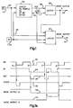
- FIG. 1 a block diagram at a relatively high level is shown of the invention for three separate operating modes according to this invention, which can be used as input to an Integrated Circuit Dynamic Random Access Memory (ID DRAM) chip.
- This circuit includes an access pad or pin 12 to which the row enable (RE) signal is supplied.
- a second pin 14 is provided which is an auxiliary input (AI).
- a sample and hold circuit 20 is provided to sample the AI at pin 14 state when RE, pin 12, transitions to an active logic low state.
- An example of a sample and hold circuit 20 is shown in Figure 3.
- the circuit 20 is a single shot output, which includes a series of inverters 21a, 21b and 21c connected to NOR gate 21d.
- the NOR gate 21d is connected to a pair of NAND gates 21e and 21f, which gates are interconnected by an invertor 21g.
- the output is gated to through NAND gate 21e wherever the AI at pin 14 is at low logic state and gated through NAND gate 21f whenever the AI at pin 14 is in the high logic state.
- the pin 12 is connected through line 22 to the circuit 20 and the pin 14 is connected to the circuit 20 through line 24.
- One output from the circuit 20 is connected from gate 21e through line 26 to a latch 28.
- the purpose of this latch is to remain in a given condition unless actuated by a signal.
- An example of the latch 28 is shown in Figure 4.
- the latch 28 includes a pair of negative AND (NAND) gates 29a and 29b.
- the line 26 is used for a set signal to be given as will be described presently.
- a line 30 is also connected from the gate 21f of circuit 20 to the latch 28, which is used for a reset signal, which will also be described presently.
- a line 22 is provided, which connects pin 12 to a latch 34.
- An example of latch 34 is shown in Figure 5.
- Latch 34 includes a pair of inverters 35a and 35b connected to a NAND gate 35c which in turn is connected to NAND gates 35d and 35e.
- Line 24 also connects the AI at pin 14 to the latch 34.
- Line 30 connects the reset side of the circuit 20 to the latch 34.
- Latch 28 has an output line 40, which is connected to the latch 34.
- the line 40 will be referred to as the mode output A line, and it is the condition of this line which determines whether the chip is in the Page mode or Static Column mode.
- Latch 34 also has a line 44 which will be referred to as mode output B line. This line provides a signal that indicates (in conjunction with the signal on the mode output A line) the third and fourth DRAM operating modes.
- FIG. 1A a timing diagram or pulse diagram of the phases, is shown. Each of the phases represents whether the line is in a logic "high” or logic “low” state.
- the Row Enable line 22 pulses between an active low state and an inactive high state.
- the state of the AI line 24, in combination with the RE line 22, is used to establish the mode of operation.
- the SET line 26 and the RESET line 30 are responsive through circuit 20 to both the RE line 22 and AI line 24.
- the Mode Output A line 40 is responsive to latch 28, and the Mode Output B line 44 is responsive to latch 34. This can be seen in the diagram of Figure 1.
- Figure 1A assumes a default mode with lines 22, 24, 26, 30 and 40 in a high state and Mode Output B line 44 in a low state.
- Row Enable line 22 goes low as shown at A indicating a circuit selection
- RESET pulse is generated, detecting that AI line 24 was at a high state.
- Output lines 40 and 44 remain in their original reset or default states, and the mode of operation does not change.
- output line 40 can be switched back and forth between two desired modes of operation.
- second output line 44 which is held low during the selection of the first two modes, can be changed to a high state to provide a third mode of operation with respect to the line 40.
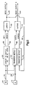
- FIG. 2 a circuit with four-way operation for four operating modes is shown.
- RE Row Enable
- Circuit 20 which is the same as circuit 20 in Figure 1, (in combination with latch 60 which will be described presently) will provide a sample and hold of the state of the AI pin 14.
- Line 22 connects the pad 12 to the circuit 20 and line 24 connects the AI pad 14 to the circuit 20.
- AI pad 14 is also connected by line 24 to a transition detect circuit 52.
- An example of transition detect circuit 52 is shown in Figure 6.
- the circuit 52 includes inverters 59a, 59b and 59c connected in series with each other and to a NAND gate 59d and a NOR gate 59e connected in parallel with each other.
- Gate 59e is connected directly to NOR gate 59f and gate 59d is connected through inverter 59g to gate 59f, which in turn is connected through NOR gate 59h to inverter 59i.
- the Row Enable pad 14 is also connected to the gate 59h of transition detect circuit 52 by line 22.
- the circuit 20 has an output line 56 which is labeled as "Set 1” and an output line 58 labeled "Reset 1", both of which are connected to a latch 60, which is similar in design to the latch 28 shown in Figures 1 and 4.
- the transition detect circuit 52 is connected by line 62, which is labeled as "Set 2", to a latch 64 which is similar to latch 60.
- a pulse on line 62 is generated only when the RE line 22 is in a "low” logic state coinciding with a "high to low” or “low to high” logic transition on AI lines 24.
- Latch 60 provides output 40
- latch 64 provides output 44.
- Line 40 in conjunction with line 44 can represent four separate modes, which will now be described with respect to the timing diagram shown in Figure 2A.
- Figure 2A assumes an initial condition for the circuits in Figure 2 having lines 22, 24, 56, 58, 62 and 74 in a high state, and having lines 40 and 44 in a low state.
- the RE line 22 goes low as shown at M
- the Reset 1 line 58 is actuated
- Latch 60 returns to a reset state with line 40 changing to a high state.
- the transition on line 40 actuates a transition detector 72.
- Transition detector 72 includes Inverters 73a, 73b and 73c connected in series to NAND gate 73d and NOR gate 73e which are connected in parallel.
- NOR gate 73e is connected directly to NOR gate 73f
- an NAND gate 73d is connected through inverter 73g to NOR gate 73f.
- Latch 64 returns to a reset state with line 44 changing to a high state.
- Lines 40 and 44 are now set to state 1. If in this first state RE is received as shown at N, this will actuate reset 1 line 58 only, which will not cause either the lines 40 or 44 to change from state 1. However, if the AI line 24 goes low prior to line 22 going low (as at P), this will actuate the Set 1 line 56 and in turn the Reset 2 line 74. The Set 1 line 56 will cause the line 40 to go low and the Reset 2 line will maintain the line 44 high, thus, giving a "second" state wherein line 40 is low and line 44 is high.
Landscapes
- Engineering & Computer Science (AREA)
- Microelectronics & Electronic Packaging (AREA)
- Computer Hardware Design (AREA)
- Dram (AREA)
Claims (8)
- Procédé pour établir différents modes d'exploitation d'un composant mémoire, caractérisé en ce qu'il comprend les étapes consistant à :
contrôler l'état de tension sur une première entrée du composant mémoire lorsqu'un signal de validation a été reçu sur une deuxième entrée du composant mémoire; exploiter le composant mémoire dans un premier mode d'exploitation par défaut si l'état de tension de la première entrée est à une première valeur; exploiter le composant mémoire dans un deuxième mode d'exploitation si l'état de tension de la première entrée est à une deuxième valeur différente de la première valeur; et exploiter le composant mémoire dans un troisième mode d'exploitation si l'état de tension de la première entrée varie alors que le signal de validation est reçu et maintenu actif sur la deuxième entrée. - Procédé selon la revendication 1, caractérisé en ce que :
le composant mémoire est replacé dans le premier mode si le signal de validation est reçu sur la deuxième entrée lorsque l'état de tension de la première entrée est à ladite première valeur. - Procédé selon la revendication 1 ou 2, caractérisé en ce qu'il comprend les étapes consistant à :
exploiter la mémoire dans ledit troisième mode d'exploitation si l'état de tension de la première entrée passe de la première valeur à la deuxième valeur alors que le signal de validation est reçu et maintenu actif sur la deuxième entrée; et exploiter la mémoire dans un quatrième mode d'opération si l'état de tension sur la première entrée passe de la deuxième valeur à la première valeur tandis que le signal de validation est reçu et maintenu actif sur la deuxième entrée. - Dispositif pour établir différents modes d'exploitation d'un composant mémoire en réponse à des variations dans des états de tension, caractérisé en ce qu'il comprend :
un élément pour contrôler l'état de tension sur la plage de connexion d'une première entrée; un élément pour contrôler l'état de tension lorsqu'un signal de validation est reçu sur la plage de connexion d'une deuxième entrée; un circuit connecté à ladite première et à ladite deuxième plage de connexion pour fournir, si ledit signal de validation est reçu, un premier ensemble de signaux de sortie au composant mémoire si l'état de tension sur la première plage de connexion est à une première valeur, et un deuxième ensemble de signaux de sortie si l'état de tension de la première plage de connexion est à une deuxième valeur différente de la première valeur, et un troisième ensemble de signaux de sortie si l'état de tension de la plage de connexion de la première entrée varie alors que le signal de validation est reçu et maintenu actif sur ladite deuxième plage de connexion. - Dispositif selon la revendication 4, caractérisé en ce qu'il comprend :
un élément pour replacer le composant mémoire dans le premier mode si le signal de validation est reçu sur la deuxième entrée lorsque l'état de tension de la première entrée est à ladite première valeur. - Dispositif selon la revendication 5, caractérisé en ce qu'il comprend :
une bascule de retenue pour maintenir ledit circuit dans le mode d'exploitation sélectionné. - Dispositif selon la revendication 5, caractérisé en ce qu'il comprend :
un échantillonneur pour détecter les impulsions de tension à l'arrivée. - Dispositif selon l'une quelconque des revendications 4 à 7, caractérisé en ce que ledit circuit fournit ledit troisième ensemble de signaux de sortie si l'état de tension de la première plage de connexion passe de la première valeur à la deuxième valeur alors que le signal de validation est reçu et maintenu actif sur ladite deuxième plage de connexion, et un quatrième ensemble de signaux de sortie si l'état de tension sur la première plage de connexion passe de la deuxième valeur à la première valeur tandis que le signal de validation est reçu et maintenu actif sur ladite deuxième plage de connexion.
Applications Claiming Priority (2)
| Application Number | Priority Date | Filing Date | Title |
|---|---|---|---|
| US07/469,880 US5036495A (en) | 1989-12-28 | 1989-12-28 | Multiple mode-set for IC chip |
| US469880 | 1999-12-22 |
Publications (3)
| Publication Number | Publication Date |
|---|---|
| EP0447624A2 EP0447624A2 (fr) | 1991-09-25 |
| EP0447624A3 EP0447624A3 (en) | 1992-05-13 |
| EP0447624B1 true EP0447624B1 (fr) | 1995-10-11 |
Family
ID=23865410
Family Applications (1)
| Application Number | Title | Priority Date | Filing Date |
|---|---|---|---|
| EP90122037A Expired - Lifetime EP0447624B1 (fr) | 1989-12-28 | 1990-11-17 | Sélection multiple de fonctionnement de mémoire pour chip de mémoire IC |
Country Status (4)
| Country | Link |
|---|---|
| US (1) | US5036495A (fr) |
| EP (1) | EP0447624B1 (fr) |
| JP (1) | JPH03203086A (fr) |
| DE (1) | DE69022975T2 (fr) |
Families Citing this family (8)
| Publication number | Priority date | Publication date | Assignee | Title |
|---|---|---|---|---|
| US5305283A (en) * | 1990-04-06 | 1994-04-19 | Mosaid, Inc. | Dram column address latching technique |
| US6324120B2 (en) | 1990-04-18 | 2001-11-27 | Rambus Inc. | Memory device having a variable data output length |
| US6751696B2 (en) | 1990-04-18 | 2004-06-15 | Rambus Inc. | Memory device having a programmable register |
| IL96808A (en) | 1990-04-18 | 1996-03-31 | Rambus Inc | Introductory / Origin Circuit Agreed Using High-Performance Brokerage |
| DE69120483T2 (de) * | 1990-08-17 | 1996-11-14 | Sgs Thomson Microelectronics | Halbleiter-Speicher mit unterdrücktem Testmodus-Eingang während des Strom-Einschaltens |
| JP3344494B2 (ja) * | 1993-03-23 | 2002-11-11 | インターナショナル・ビジネス・マシーンズ・コーポレーション | ページモードを有するシングルクロックメモリ |
| US5457659A (en) * | 1994-07-19 | 1995-10-10 | Micron Technology, Inc. | Programmable dynamic random access memory (DRAM) |
| JP3351953B2 (ja) * | 1996-03-19 | 2002-12-03 | 富士通株式会社 | モードレジスタ制御回路およびこれを有する半導体装置 |
Family Cites Families (6)
| Publication number | Priority date | Publication date | Assignee | Title |
|---|---|---|---|---|
| US4159541A (en) * | 1977-07-01 | 1979-06-26 | Ncr Corporation | Minimum pin memory device |
| JPS60211555A (ja) * | 1984-04-04 | 1985-10-23 | Ascii Corp | メモリインタフエ−ス回路 |
| JPH0799616B2 (ja) * | 1984-08-30 | 1995-10-25 | 三菱電機株式会社 | 半導体記憶装置 |
| JPS61239491A (ja) * | 1985-04-13 | 1986-10-24 | Fujitsu Ltd | 電子装置 |
| US4845664A (en) * | 1986-09-15 | 1989-07-04 | International Business Machines Corp. | On-chip bit reordering structure |
| JPH01205788A (ja) * | 1988-02-12 | 1989-08-18 | Toshiba Corp | 半導体集積回路 |
-
1989
- 1989-12-28 US US07/469,880 patent/US5036495A/en not_active Expired - Fee Related
-
1990
- 1990-11-17 DE DE69022975T patent/DE69022975T2/de not_active Expired - Fee Related
- 1990-11-17 EP EP90122037A patent/EP0447624B1/fr not_active Expired - Lifetime
- 1990-11-28 JP JP2323418A patent/JPH03203086A/ja active Pending
Also Published As
| Publication number | Publication date |
|---|---|
| EP0447624A2 (fr) | 1991-09-25 |
| EP0447624A3 (en) | 1992-05-13 |
| US5036495A (en) | 1991-07-30 |
| JPH03203086A (ja) | 1991-09-04 |
| DE69022975T2 (de) | 1996-05-30 |
| DE69022975D1 (de) | 1995-11-16 |
Similar Documents
| Publication | Publication Date | Title |
|---|---|---|
| US5408435A (en) | Semiconductor memory with inhibited test mode entry during power-up | |
| US5161159A (en) | Semiconductor memory with multiple clocking for test mode entry | |
| EP0471542A2 (fr) | Circuit amélioré de remise à zéro à la mise sous tension pour commander l'entrée en mode de test | |
| EP0471543B1 (fr) | Mémoire à semi-conducteur à code d'accès rhytmé pour entrée dans le mode de test | |
| US5659508A (en) | Special mode enable transparent to normal mode operation | |
| US6061282A (en) | Semiconductor memory having an improved test circuit | |
| EP0174236B1 (fr) | Circuit intégré à semi-conducteur comportant un circuit d'essai | |
| US5134587A (en) | Semiconductor memory with automatic test mode exit on chip enable | |
| KR100206677B1 (ko) | 테스트 회로가 설치된 반도체 메모리 | |
| EP0447624B1 (fr) | Sélection multiple de fonctionnement de mémoire pour chip de mémoire IC | |
| US5841784A (en) | Testing and repair of embedded memory | |
| US20020080668A1 (en) | Current controlled multi-state parallel test for semiconductor device | |
| US5889713A (en) | Testing of embedded memory by coupling the memory to input/output pads using switches | |
| US5134586A (en) | Semiconductor memory with chip enable control from output enable during test mode | |
| US7123069B2 (en) | Latch or phase detector device | |
| US6546510B1 (en) | Burn-in mode detect circuit for semiconductor device | |
| EP0675597B1 (fr) | Circuit intégré et méthode avec contrÔle centralisé de la durée d'impulsions de détection de transition de flanc | |
| US5818768A (en) | Operation mode setting circuit in semiconductor device | |
| KR20010014986A (ko) | 반도체 기억 장치 및 번인 테스트 방법 | |
| DE69721361T2 (de) | Einchipspeichersystem mit einem Dekoder für Pulswortleitungsverfahren | |
| EP0170912B1 (fr) | Circuit intégré avec une borne d'entrée commune | |
| KR19990044773A (ko) | 반도체 집적 회로 장치 | |
| US6158029A (en) | Method of testing an integrated circuit having a memory and a test circuit | |
| US6320814B1 (en) | Semiconductor device | |
| KR100800132B1 (ko) | 반도체 메모리 장치의 테스트 모드 엔트리 방법 및 이를 이용한 테스트 모드 신호선이 배치된 반도체 메모리 장치 |
Legal Events
| Date | Code | Title | Description |
|---|---|---|---|
| PUAI | Public reference made under article 153(3) epc to a published international application that has entered the european phase |
Free format text: ORIGINAL CODE: 0009012 |
|
| AK | Designated contracting states |
Kind code of ref document: A2 Designated state(s): DE FR GB |
|
| 17P | Request for examination filed |
Effective date: 19911018 |
|
| PUAL | Search report despatched |
Free format text: ORIGINAL CODE: 0009013 |
|
| AK | Designated contracting states |
Kind code of ref document: A3 Designated state(s): DE FR GB |
|
| 17Q | First examination report despatched |
Effective date: 19940531 |
|
| GRAA | (expected) grant |
Free format text: ORIGINAL CODE: 0009210 |
|
| AK | Designated contracting states |
Kind code of ref document: B1 Designated state(s): DE FR GB |
|
| PGFP | Annual fee paid to national office [announced via postgrant information from national office to epo] |
Ref country code: FR Payment date: 19951107 Year of fee payment: 6 |
|
| REF | Corresponds to: |
Ref document number: 69022975 Country of ref document: DE Date of ref document: 19951116 |
|
| PGFP | Annual fee paid to national office [announced via postgrant information from national office to epo] |
Ref country code: DE Payment date: 19951123 Year of fee payment: 6 |
|
| ET | Fr: translation filed | ||
| PLBE | No opposition filed within time limit |
Free format text: ORIGINAL CODE: 0009261 |
|
| STAA | Information on the status of an ep patent application or granted ep patent |
Free format text: STATUS: NO OPPOSITION FILED WITHIN TIME LIMIT |
|
| 26N | No opposition filed | ||
| PGFP | Annual fee paid to national office [announced via postgrant information from national office to epo] |
Ref country code: GB Payment date: 19961028 Year of fee payment: 7 |
|
| PG25 | Lapsed in a contracting state [announced via postgrant information from national office to epo] |
Ref country code: FR Effective date: 19970731 |
|
| PG25 | Lapsed in a contracting state [announced via postgrant information from national office to epo] |
Ref country code: DE Effective date: 19970801 |
|
| REG | Reference to a national code |
Ref country code: FR Ref legal event code: ST |
|
| PG25 | Lapsed in a contracting state [announced via postgrant information from national office to epo] |
Ref country code: GB Free format text: LAPSE BECAUSE OF NON-PAYMENT OF DUE FEES Effective date: 19971117 |
|
| GBPC | Gb: european patent ceased through non-payment of renewal fee |
Effective date: 19971117 |