EP0447638B1 - A method for manufacturing a thermal head - Google Patents
A method for manufacturing a thermal head Download PDFInfo
- Publication number
- EP0447638B1 EP0447638B1 EP90124005A EP90124005A EP0447638B1 EP 0447638 B1 EP0447638 B1 EP 0447638B1 EP 90124005 A EP90124005 A EP 90124005A EP 90124005 A EP90124005 A EP 90124005A EP 0447638 B1 EP0447638 B1 EP 0447638B1
- Authority
- EP
- European Patent Office
- Prior art keywords
- lead electrodes
- strip
- resistor
- resistors
- thermal head
- Prior art date
- Legal status (The legal status is an assumption and is not a legal conclusion. Google has not performed a legal analysis and makes no representation as to the accuracy of the status listed.)
- Expired - Lifetime
Links
Images


Classifications
-
- B—PERFORMING OPERATIONS; TRANSPORTING
- B41—PRINTING; LINING MACHINES; TYPEWRITERS; STAMPS
- B41J—TYPEWRITERS; SELECTIVE PRINTING MECHANISMS, i.e. MECHANISMS PRINTING OTHERWISE THAN FROM A FORME; CORRECTION OF TYPOGRAPHICAL ERRORS
- B41J2/00—Typewriters or selective printing mechanisms characterised by the printing or marking process for which they are designed
- B41J2/315—Typewriters or selective printing mechanisms characterised by the printing or marking process for which they are designed characterised by selective application of heat to a heat sensitive printing or impression-transfer material
- B41J2/32—Typewriters or selective printing mechanisms characterised by the printing or marking process for which they are designed characterised by selective application of heat to a heat sensitive printing or impression-transfer material using thermal heads
-
- B—PERFORMING OPERATIONS; TRANSPORTING
- B41—PRINTING; LINING MACHINES; TYPEWRITERS; STAMPS
- B41J—TYPEWRITERS; SELECTIVE PRINTING MECHANISMS, i.e. MECHANISMS PRINTING OTHERWISE THAN FROM A FORME; CORRECTION OF TYPOGRAPHICAL ERRORS
- B41J2/00—Typewriters or selective printing mechanisms characterised by the printing or marking process for which they are designed
- B41J2/315—Typewriters or selective printing mechanisms characterised by the printing or marking process for which they are designed characterised by selective application of heat to a heat sensitive printing or impression-transfer material
- B41J2/32—Typewriters or selective printing mechanisms characterised by the printing or marking process for which they are designed characterised by selective application of heat to a heat sensitive printing or impression-transfer material using thermal heads
- B41J2/345—Typewriters or selective printing mechanisms characterised by the printing or marking process for which they are designed characterised by selective application of heat to a heat sensitive printing or impression-transfer material using thermal heads characterised by the arrangement of resistors or conductors
-
- Y—GENERAL TAGGING OF NEW TECHNOLOGICAL DEVELOPMENTS; GENERAL TAGGING OF CROSS-SECTIONAL TECHNOLOGIES SPANNING OVER SEVERAL SECTIONS OF THE IPC; TECHNICAL SUBJECTS COVERED BY FORMER USPC CROSS-REFERENCE ART COLLECTIONS [XRACs] AND DIGESTS
- Y10—TECHNICAL SUBJECTS COVERED BY FORMER USPC
- Y10T—TECHNICAL SUBJECTS COVERED BY FORMER US CLASSIFICATION
- Y10T29/00—Metal working
- Y10T29/49—Method of mechanical manufacture
- Y10T29/49002—Electrical device making
- Y10T29/49082—Resistor making
- Y10T29/49083—Heater type
-
- Y—GENERAL TAGGING OF NEW TECHNOLOGICAL DEVELOPMENTS; GENERAL TAGGING OF CROSS-SECTIONAL TECHNOLOGIES SPANNING OVER SEVERAL SECTIONS OF THE IPC; TECHNICAL SUBJECTS COVERED BY FORMER USPC CROSS-REFERENCE ART COLLECTIONS [XRACs] AND DIGESTS
- Y10—TECHNICAL SUBJECTS COVERED BY FORMER USPC
- Y10T—TECHNICAL SUBJECTS COVERED BY FORMER US CLASSIFICATION
- Y10T29/00—Metal working
- Y10T29/49—Method of mechanical manufacture
- Y10T29/49002—Electrical device making
- Y10T29/49082—Resistor making
- Y10T29/49101—Applying terminal
Definitions
- the present invention relates to a method for manufacturing a thermal head for half-tone printing.
- Thermal heads with a novel faculty have been intensively developed of late such that half-tone printing can be effected by changing the size of printing dots to be printed.
- Such thermal heads are disclosed in "Half Tone Wax Transfer Using a Novel Thermal Head", THE FOURTH INTERNATIONAL CONGRESS ON ADVANCES IN NON-IMPACT PRINTING TECHNOLOGIES pp. 273-276, "Thermo-Convergent Ink-Transfer Printing (TCIP) for Full Color Reproduction", Proceedings of 2nd Non-impact Printing Technologies Symposium pp. 105-108, “Published Unexamined Japanese Patent Application Nos. 60-58877 and 60-78768".
- Each of the thermal heads is provided with a number of heating resistors each having a narrow-width portion.
- each heating resistor increases its density at the narrow-width portion, so that heat is produced from a local region in the high-density portion.
- thermal heads only those regions which produce heat higher than a certain value are effective for printing, and the regions capable of generating sufficient heat for the printing spread in proportion to voltage applied to the heating resistors. If higher voltage is applied to the heating resistors, therefore, the size of the printing dots increases in proportion.
- the heating resistors have a complicated configuration, so that manufacturing them requires much time and labor, and it is difficult to provide uniform properties for the numerous heating resistors.
- the present inventors proposed a thermal head designed for half-tone printing and including a plurality of parallelogrammatic resistors (cf. EP-A-0 410 486).
- Prior art document EP-A-0 211 331 discloses a method of manufacturing a heat-sensitive recording head wherein first and second electrodes, to which a recording signal is to be applied, are printed to a desired pattern on an insulating substrate by a screen printing method.
- a heating resistor is formed by the screen printing method so as to be bridged over these first and second electrodes.
- a protective layer is formed so as to cover the first and second electrodes and the heating resistor therewith.
- Each of the heating portions of the heating resistor is provided with one of a plurality of laser-made holes, and the resistance value of each heating portion of the heating resistor is regulated to a predetermined level on the basis of the number of the laser-made holes.
- An object of the present invention is to provide a method for easily manufacturing such a thermal head at low cost.
- the present invention provides a method as specified in claim 1.
- the thermal head which has a plurality of parallelogromatic resistors along its main scanning axis is fabricated as follows.
- a plurality of lead electrodes are formed on an insulating substrate such that the lead electrodes are arranged at regular intervals in parallel to one another and extend diagonally with respect to the main scanning axis.
- at least one strip-shaped resistor is formed on the resultant structure to extend along the main scanning axis and across the lead electrodes, whereby the thermal head is obtained.
- each area defined by any two adjacent lead electrodes and a pair of opposite side edges of the strip-shpaed resistor forms a parallelogrammatic resistor.
- a thermal head 10 comprises a plurality of a parallelogrammatic resistors 14p formed on an insulating substrate 12 and arranged in the direction of the main scanning axis, i.e., in the longitudinal direction of the substrate 12.
- Each parallelogrammatic resistor 14p has its one pair of opposite sides connected to lead electrodes 16 and 18, respectively, and constitutes one heating resistor used for recording one pixel.
- the lead electrodes 16 are connected together, thus constituting a common electrode.
- the thermal head 10 is fabricated as follows. First, a substantially rectangular insulating substrate 12 is prepared. As is shown in Figs. 2 and 3, the insulating substrate 12 has a laminated structure made up of: a support layer 22, a base layer 24, and a glaze layer 26, for example. Next, pairs of parallel lead electrodes 16 and 18 are formed on the insulating substrate 12 such that they extend slantwise with reference to the direction of the main scanning axis and such that they are spaced from each other at regular intervals. The lead electrodes 16 and 18 are formed by use of a lithography technology, including deposition and etching.
- a strip-shaped resistor 14 extending in the direction of the main scanning axis is formed on the insulating substrate 12 by coating the insulating substrate 12 with paste of a heating resistor material by screen printing. Finally, a protective layer 32 is formed on the resultant structure, so as to prevent the resistor 14 and the lead electrodes 16 and 18 from being oxidized or worn away.
- each of those portions of the strip-shaped resistor which are defined by a pair of lead electrodes 16 and 18 serves as a parallelogrammatic heating resistor 14p used for recording one pixel.
- a current flows through the heating resistors 14p, so that the resistors 14p are heated.
- Fig. 4 shows current distribution in the resistors 14p.
- black spots represent points of measurement
- the direction of each line indicates the direction of electric current at each corresponding measurement point
- the length of the line indicates the magnitude of the current at the measurement point.
- each resistor 14p is formed of a thin film whose thickness is so small that it is negligible.
- the current distribution is supposed to be two-dimensional.
- equation (6) will now be numerically analyzed.
- the boundary element method as shown in Fig. 5, the boundary of a closed system is divided into elements, which are calculated using predetermined boundary conditions so that the solutions of all the elements are obtained.
- the internal conditions of the system are detected.
- the current distribution shown in Fig. 4 is obtained.
- the heat release value at a certain point on the resistor 14p can be represented by the product of the square of the current value at that position and the resistance value of the resistor 14p. Namely, the heat release value is proportional to the square of the current value. Thus, the heat value is large at the central portion of the heating resistor 14p.
- recording of printing dots requires a fixed amount of heat or more. If the voltage applied to the heating resistor 14p is low, therefore, the printing dots are recorded by heating within a range indicated by numeral 30a in Fig. 4. As the applied voltage is increased, the printing dots start to be recorded by heating within ranges indicated by numerals 30b and 30c.
- the virtual heating area can be varied as indicated by 30a, 30b and 30c in Fig. 4, for example, so that the size of the printing dots can be modulated.
- the current distribution in the heating resistor 14p varies depending on the shape of the resistor, and there is a resistor shape for optimum gradation recording.
- This is a shape which enables heat concentration to a certain degree or higher.
- Parameters indicative of a parallelogrammatic shape include the ratio g between the respective lengths La and Lb of sides 14a and 14b and the angle 8 (acute angle in this case) formed between the sides 14a and 14b, as shown in Fig. 6.
- the thermal head is applied to a standard-G3 facsimile.
- the 12 shapes may be classified into four types based on the combinations of the ratios g of 1. 1.5, and 2 and the angles ⁇ of 30° (type (a)), 45° (type (b)), 60° (type (c)), and 75° (type (d)).
- Figs. 7A to 7C show cases corresponding to the ratios g of 1, 1.5, and 2, respectively, for type (a), and Figs. 7D to 7F, 7G to 7I, and 7I to 7L show similar cases for types (b), (c), and (d) respectively.
- Figs. 8 to 13 show e n / ⁇ obtained by dividing the energy density e n , calculated according to equation (7) on the basis of the obtained electric fields E, by the electric conductivity o.
- Figs. 8 and 9 show cases corresponding to the horizontal and diagonal directions, respectively, for the ratio g of 1
- Figs. 10 and 11 show similar cases for the ratio g of 1.5
- Figs. 12 and 13 show similar cases for the ratio g of 2.
- Figs. 8 to 13 indicate the following circumstances. If the ratio g is 2 (Figs. 12 and 13), the energy distribution is substantially uniform, and there is hardly any energy concentration. If the ratio g is 1.5. some energy concentration is caused. If the ratio g is 1, a considerable energy concentration is entailed. As seen from Figs. 8 and 9, moreover, if the ratio g is 1, the energy concentration is conspicuous when the angle ⁇ is 45° or less.
- each heating resistor 14p the conditions for providing each heating resistor 14p are: g ⁇ 1, and ⁇ ⁇ 45°. Since the width La of the heating resistor is 100 »m, the height h thereof (height: the length defined in the sub-scanning direction) is defined by h ⁇ 100/ ⁇ 2 »m. That is, the height of the resistor is no more than 71 »m or so.
- a heating resistor having such dimensions is suitable in the case where the resolution in the sub-scanning direction is higher than 15.4 lines/mm.
- the resolutions normally available in a G3-type facsimile machine are: 8 dots/mm ⁇ 7.7 lines/mm, 8 dots/mm ⁇ 3.85 lines/mm, etc. In these cases, the resolutions in the sub-scanning direction are lower than 15.4 lines/mm.
- the thermal head of the above-mentioned embodiment is not applicable to such low-resolution recording, though it is suitable for recording with the resolution of 15.4 lines/mm.
- FIG. 14 Another type of thermal head which is suitable for low-resolution recording will be described, with reference to Fig. 14.
- the members which are similar to those used in the above-mentioned thermal head will be referred to by the same reference numerals and symbols, and a detailed description of them will be omitted herein.
- the second type of thermal head 10 comprises an insulating substrate 12, and two strip-shaped resistors 14 which are formed on the insulating substrate 12 and extend in parallel to each other in the direction of the main scanning axis.
- the two strip-shaped resistors 14 are spaced from each other by a predetermined short distance.
- the strip-shaped resistors 14 are formed on the substrate by coating the insulating substrate 12 with paste of a heat-generating resistor material by screen printing.
- the thermal head 10 also comprises a pair of lead electrodes 16 and 18 which extend in parallel to each other and cross the two strip-shaped resistors 14 slantwise.
- each of those portions of the strip-shaped resistor 14 which are defined by a pair of lead electrodes 16 and 18 serves as a parallelogrammatic heating resistor 14p used for recording one printing dot.
- Each heating resistor 14p satisfies the above-mentioned optimal conditions: namely, g ⁇ 1, and ⁇ ⁇ 45°.
- the adjacent heating resistors 14p that are connected in common to the same two lead electrodes 16 and 18 function as one heat-generating section used for recording one pixel. If it is assumed that each heating resistor 14p has a width of 100 »m, a height of 70 »m and an angle of 45°, then the height of the heat-generating section is about 140 »m, which is a value corresponding to 7.7 lines/mm.
- each heating resistor 14p satisfies the optimal conditions mentioned above, so that its heat-generating characteristic is suitable for half-tone printing. Therefore, satisfactory half-tone printing can be performed with a resolution of 8 dots/mm ⁇ 7.7 lines/mm.
- the number of strip-shaped resistors 14 is four, recording can be performed with a resolution of 8 dots/mm ⁇ 3.85 lines/mm. In this way, an arbitrary resolution may be obtained by changing the number of strip-shaped resistors 14.
- the centers of the two parallelogrammatic resistors 14p which jointly records one pixel are shifted by ⁇ in the direction of the main scanning axis. Therefore, the two printing dots corresponding to one pixel are shifted by ⁇ in the main scanning direction. In some cases, this may result in a certain degree of deterioration in the quality of an image.
- the thermal head 10 comprises a pair of parallel strip-shaped resistors 14 extending in the direction of the main scanning axis, and two parallel lead electrodes 16 and 18 diagonally crossing the strip-shaped resistors 14.
- each of the lead electrodes 16 and 18 is bent at an intermediate point thereof such that it is substantially "L"-shaped.
- a parallelogrammatic heating resistor 14p is defined by the adjacent ones of the substantially "L"-shaped lead electrodes 16 and 18. In the case where slanting sides of the heating resistor 14p are slanted 45°, the angle at which the lead electrodes 16 and 18 are bent is 90°.
- the two heating resistors 14p which are defined by such lead electrodes and which are jointly used for printing one pixel are at the same location in the direction of the main scanning axis. Therefore, satisfactory half-tone printing is ensured with a resolution of 8 dots/mm ⁇ 7.7 lines/mm, without resulting in deterioration in the quality of an image.
Landscapes
- Electronic Switches (AREA)
Description
- The present invention relates to a method for manufacturing a thermal head for half-tone printing.
- Thermal heads with a novel faculty have been intensively developed of late such that half-tone printing can be effected by changing the size of printing dots to be printed. Such thermal heads are disclosed in "Half Tone Wax Transfer Using a Novel Thermal Head", THE FOURTH INTERNATIONAL CONGRESS ON ADVANCES IN NON-IMPACT PRINTING TECHNOLOGIES pp. 273-276, "Thermo-Convergent Ink-Transfer Printing (TCIP) for Full Color Reproduction", Proceedings of 2nd Non-impact Printing Technologies Symposium pp. 105-108, "Published Unexamined Japanese Patent Application Nos. 60-58877 and 60-78768". Each of the thermal heads is provided with a number of heating resistors each having a narrow-width portion. Electric current flowing through each heating resistor increases its density at the narrow-width portion, so that heat is produced from a local region in the high-density portion. In thermal heads, only those regions which produce heat higher than a certain value are effective for printing, and the regions capable of generating sufficient heat for the printing spread in proportion to voltage applied to the heating resistors. If higher voltage is applied to the heating resistors, therefore, the size of the printing dots increases in proportion.
- In the conventional thermal head of this type, however, the heating resistors have a complicated configuration, so that manufacturing them requires much time and labor, and it is difficult to provide uniform properties for the numerous heating resistors.
- To provide a solution to the above-mentioned problems, the present inventors proposed a thermal head designed for half-tone printing and including a plurality of parallelogrammatic resistors (cf. EP-A-0 410 486).
- Prior art document EP-A-0 211 331 discloses a method of manufacturing a heat-sensitive recording head wherein first and second electrodes, to which a recording signal is to be applied, are printed to a desired pattern on an insulating substrate by a screen printing method. A heating resistor is formed by the screen printing method so as to be bridged over these first and second electrodes. A protective layer is formed so as to cover the first and second electrodes and the heating resistor therewith. Each of the heating portions of the heating resistor is provided with one of a plurality of laser-made holes, and the resistance value of each heating portion of the heating resistor is regulated to a predetermined level on the basis of the number of the laser-made holes.
- An object of the present invention is to provide a method for easily manufacturing such a thermal head at low cost.
- To solve this object the present invention provides a method as specified in
claim 1. - The thermal head which has a plurality of parallelogromatic resistors along its main scanning axis is fabricated as follows. A plurality of lead electrodes are formed on an insulating substrate such that the lead electrodes are arranged at regular intervals in parallel to one another and extend diagonally with respect to the main scanning axis. Then, at least one strip-shaped resistor is formed on the resultant structure to extend along the main scanning axis and across the lead electrodes, whereby the thermal head is obtained. In this thermal head, each area defined by any two adjacent lead electrodes and a pair of opposite side edges of the strip-shpaed resistor forms a parallelogrammatic resistor.
- This invention can be more fully understood from the following detailed description when taken in conjunction with the accompanying drawings, in which:
- Fig. 1 is a view of a thermal head manufactured by use of a method embodying the present invention;
- Fig. 2 is a sectional view taken along line II-II in Fig. 1;
- Fig. 3 is a sectional view taken along line III-III in Fig. 1;
- Fig. 4 is a view illustrating how current is distributed and how heat is generated in a heating resistor shown in Fig. 1;
- Fig. 5 is an explanatory view of a boundary element method;
- Fig. 6 shows the factors for defining the shape of a parallelogrammatic resistor;
- Figs. 7A-7L are views showing how current is distributed in each of various-shape parallelogrammatic resistors, the views in Figs. 7A-7L being obtained by the boundary element method;
- Figs. 8-13 are graphs showing energy distributions obtained by calculation;
- Fig. 14 shows the structure of a thermal head suitable for low-resolution recording; and
- Fig. 15 shows the structure of an improved thermal head suitable for low-resolution recording.
- An embodiment of the present invention will now be described, with reference to the accompanying drawings.
- Referring first to Fig. 1, a
thermal head 10 comprises a plurality of aparallelogrammatic resistors 14p formed on aninsulating substrate 12 and arranged in the direction of the main scanning axis, i.e., in the longitudinal direction of thesubstrate 12. Eachparallelogrammatic resistor 14p has its one pair of opposite sides connected tolead electrodes lead electrodes 16 are connected together, thus constituting a common electrode. - The
thermal head 10 is fabricated as follows. First, a substantially rectangularinsulating substrate 12 is prepared. As is shown in Figs. 2 and 3, theinsulating substrate 12 has a laminated structure made up of: asupport layer 22, abase layer 24, and aglaze layer 26, for example. Next, pairs ofparallel lead electrodes insulating substrate 12 such that they extend slantwise with reference to the direction of the main scanning axis and such that they are spaced from each other at regular intervals. Thelead electrodes shaped resistor 14 extending in the direction of the main scanning axis is formed on theinsulating substrate 12 by coating theinsulating substrate 12 with paste of a heating resistor material by screen printing. Finally, aprotective layer 32 is formed on the resultant structure, so as to prevent theresistor 14 and thelead electrodes thermal head 10 fabricated as above, each of those portions of the strip-shaped resistor which are defined by a pair oflead electrodes parallelogrammatic heating resistor 14p used for recording one pixel. - When a voltage from a
variable voltage source 28 is applied between thelead electrodes heating resistors 14p, so that theresistors 14p are heated. Fig. 4 shows current distribution in theresistors 14p. In Fig. 4, black spots represent points of measurement, the direction of each line indicates the direction of electric current at each corresponding measurement point, and the length of the line indicates the magnitude of the current at the measurement point. - The following is a description of the current distribution in the
heating resistors 14p shown in Fig. 4. Here it is supposed that the resistance values of theresistors 14p cannot be changed by heating. For example, eachresistor 14p is formed of a thin film whose thickness is so small that it is negligible. Thus, the current distribution is supposed to be two-dimensional. - Based on this supposition, the current flowing through the
heating resistors 14p is a steady-state current, which generates a static magnetic field. Since magnetic flux density B makes no time-based change, therefore, the following equation is obtained from the Maxwell equation:

where E is an electric field. Based on the principle of conservation of charge, moreover, we obtain

where i is the current density. The Ohm's law is valid for the relation between the current density i and the electric field E as follows:

where σ is electric conductivity. Substituting equation (3) into equation (2), we obtain

From equations (1) and (4), we recognizes a certain scalar function V, and the electric field E may be given by

This scalar function V is generally called as an electric potential. Substituting equation (5) into equation (4), in consideration of the two-dimensional current distribution, we obtain the following Laplace equation:
Further, energy density en is given by

By obtaining the electric field E by substituting the solution of equation (6) into equation (5), therefore, heating energy distribution can be obtained from equation (7). - Using the boundary element method, equation (6) will now be numerically analyzed. According to the boundary element method, as shown in Fig. 5, the boundary of a closed system is divided into elements, which are calculated using predetermined boundary conditions so that the solutions of all the elements are obtained. Thus, the internal conditions of the system are detected. As a result, the current distribution shown in Fig. 4 is obtained.
- As seen from Fig. 4, there are larger current flows in the regions nearer to the center of each
heating resistor 14p. The heat release value at a certain point on theresistor 14p can be represented by the product of the square of the current value at that position and the resistance value of theresistor 14p. Namely, the heat release value is proportional to the square of the current value. Thus, the heat value is large at the central portion of theheating resistor 14p. - Meanwhile, recording of printing dots requires a fixed amount of heat or more. If the voltage applied to the
heating resistor 14p is low, therefore, the printing dots are recorded by heating within a range indicated by numeral 30a in Fig. 4. As the applied voltage is increased, the printing dots start to be recorded by heating within ranges indicated by numerals 30b and 30c. - By changing the voltage applied to the
heating resistor 14p, the virtual heating area can be varied as indicated by 30a, 30b and 30c in Fig. 4, for example, so that the size of the printing dots can be modulated. - The current distribution in the
heating resistor 14p varies depending on the shape of the resistor, and there is a resistor shape for optimum gradation recording. This is a shape which enables heat concentration to a certain degree or higher. Parameters indicative of a parallelogrammatic shape include the ratio g between the respective lengths La and Lb ofsides 14a and 14b and the angle 8 (acute angle in this case) formed between thesides 14a and 14b, as shown in Fig. 6. The optimum shape can be obtained under the following conditions:


- The following is a description of the optimum shape of the
heating resistor 14p. In the example described below, the thermal head is applied to a standard-G3 facsimile. - In the standard-G3 facsimile, the resolution in the direction of the main scanning axis is specified as being 8 dots/mm, so that the width or length La of each
heating resistor 14p is
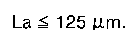
If the gap between each twoadjacent heating resistors 14p is 25 »m, La is

- Figs. 7A to 7L show various modes of current distribution obtained for 12 varied shapes by the aforementioned method using the outline of each
heating resistor 14p as a boundary, as shown in Fig. 6, under conditions including La = 100 »m and the respective electric potentials of thelead electrodes - Figs. 7A to 7C show cases corresponding to the ratios g of 1, 1.5, and 2, respectively, for type (a), and Figs. 7D to 7F, 7G to 7I, and 7I to 7L show similar cases for types (b), (c), and (d) respectively.
- The electric fields E in the horizontal and diagonal directions (see Fig. 6) are obtained for the
individual heating resistors 14p having these shapes. Figs. 8 to 13 show en/σ obtained by dividing the energy density en, calculated according to equation (7) on the basis of the obtained electric fields E, by the electric conductivity o. - Figs. 8 and 9 show cases corresponding to the horizontal and diagonal directions, respectively, for the ratio g of 1, Figs. 10 and 11 show similar cases for the ratio g of 1.5, and Figs. 12 and 13 show similar cases for the ratio g of 2.
- As seen from Figs. 7A to 7L and Figs. 8 to 13, the smaller the angle ϑ and ratio g, the more intensive the centralization of the current is. Figs. 8 to 13 indicate the following circumstances. If the ratio g is 2 (Figs. 12 and 13), the energy distribution is substantially uniform, and there is hardly any energy concentration. If the ratio g is 1.5. some energy concentration is caused. If the ratio g is 1, a considerable energy concentration is entailed. As seen from Figs. 8 and 9, moreover, if the ratio g is 1, the energy concentration is conspicuous when the angle ϑ is 45° or less.
- In light of the above, it is possible to assume that the conditions for providing each
heating resistor 14p are: g ≦ 1, and ϑ ≦ 45°. Since the width La of the heating resistor is 100 »m, the height h thereof (height: the length defined in the sub-scanning direction) is defined by h < 100/√2 »m. That is, the height of the resistor is no more than 71 »m or so. A heating resistor having such dimensions is suitable in the case where the resolution in the sub-scanning direction is higher than 15.4 lines/mm. - The resolutions normally available in a G3-type facsimile machine are: 8 dots/mm × 7.7 lines/mm, 8 dots/mm × 3.85 lines/mm, etc. In these cases, the resolutions in the sub-scanning direction are lower than 15.4 lines/mm. The thermal head of the above-mentioned embodiment is not applicable to such low-resolution recording, though it is suitable for recording with the resolution of 15.4 lines/mm.
- Another type of thermal head which is suitable for low-resolution recording will be described, with reference to Fig. 14. In Fig. 14, the members which are similar to those used in the above-mentioned thermal head will be referred to by the same reference numerals and symbols, and a detailed description of them will be omitted herein.
- The second type of
thermal head 10 comprises an insulatingsubstrate 12, and two strip-shapedresistors 14 which are formed on the insulatingsubstrate 12 and extend in parallel to each other in the direction of the main scanning axis. The two strip-shapedresistors 14 are spaced from each other by a predetermined short distance. As mentioned above, the strip-shapedresistors 14 are formed on the substrate by coating the insulatingsubstrate 12 with paste of a heat-generating resistor material by screen printing. Thethermal head 10 also comprises a pair oflead electrodes resistors 14 slantwise. As in the above-mentioned thermal head, each of those portions of the strip-shapedresistor 14 which are defined by a pair oflead electrodes parallelogrammatic heating resistor 14p used for recording one printing dot. Eachheating resistor 14p satisfies the above-mentioned optimal conditions: namely, g ≦ 1, and ϑ ≦ 45°. In the second type of thermal head, theadjacent heating resistors 14p that are connected in common to the same twolead electrodes heating resistor 14p has a width of 100 »m, a height of 70 »m and an angle of 45°, then the height of the heat-generating section is about 140 »m, which is a value corresponding to 7.7 lines/mm. - In the second type of thermal head, each
heating resistor 14p satisfies the optimal conditions mentioned above, so that its heat-generating characteristic is suitable for half-tone printing. Therefore, satisfactory half-tone printing can be performed with a resolution of 8 dots/mm × 7.7 lines/mm. - If the number of strip-shaped
resistors 14 is four, recording can be performed with a resolution of 8 dots/mm × 3.85 lines/mm. In this way, an arbitrary resolution may be obtained by changing the number of strip-shapedresistors 14. - In the thermal head shown in Fig. 14, the centers of the two
parallelogrammatic resistors 14p which jointly records one pixel are shifted by α in the direction of the main scanning axis. Therefore, the two printing dots corresponding to one pixel are shifted by α in the main scanning direction. In some cases, this may result in a certain degree of deterioration in the quality of an image. - A thermal head that gives solution to this problem will be described, with reference to Fig. 15.
- Referring to Fig. 15, the
thermal head 10 comprises a pair of parallel strip-shapedresistors 14 extending in the direction of the main scanning axis, and twoparallel lead electrodes resistors 14. As is shown in Fig. 15, each of thelead electrodes parallelogrammatic heating resistor 14p is defined by the adjacent ones of the substantially "L"-shapedlead electrodes heating resistor 14p are slanted 45°, the angle at which thelead electrodes heating resistors 14p which are defined by such lead electrodes and which are jointly used for printing one pixel are at the same location in the direction of the main scanning axis. Therefore, satisfactory half-tone printing is ensured with a resolution of 8 dots/mm × 7.7 lines/mm, without resulting in deterioration in the quality of an image.
Claims (4)
- A method for manufacturing a line-type thermal head (10) which has a main scanning axis, comprising the steps of:
forming a plurality of lead electrodes (16, 18) on an insulating substrate (12) such that the lead electrodes (16, 18) are arranged at regular intervals in parallel to one another; and
forming at least one strip-shaped resistor (14), which has parallel opposite side edges, on the insulating substrate (12) and the lead electrodes (16, 18), such that the strip-shaped resistor (14) extends along the main scanning axis and crosses the lead electrodes (16, 18),
characterized in that
said plurality of lead electrodes (16, 18) are arranged diagonally with reference to the main scanning axis, so that a non-rectangular parallelogrammatic heating resistor (14p) used for recording one pixel is defined by adjacent ones of the lead electrodes (16, 18) and the opposite side edges of the strip-shaped resistor (14). - A method according to claim 1, characterized in that said strip-shaped resistor (14) is formed by coating the insulating substrate (12) with paste of a resistor material by screen printing.
- A method according to claim 1 or 2, characterized in that two or more strip-shaped resistors (14) insulated from each other are formed by said step of forming at least one strip-shaped resistor.
- A method according to claim 3, characterized in that each of the lead electrodes (16, 18) includes a bent portion located between adjacent ones of the strip-shaped resistor (14), and a plurality of non-rectangular parallelogrammatic resistors (14p) which are defined by adjacent two lead electrodes (16, 18) and the opposite side edges of the strip-shaped resistors (14) are at the same location in the direction of the main scanning axis.
Applications Claiming Priority (2)
| Application Number | Priority Date | Filing Date | Title |
|---|---|---|---|
| JP2066958A JPH03268952A (en) | 1990-03-19 | 1990-03-19 | Thermal head |
| JP66958/90 | 1990-03-19 |
Publications (2)
| Publication Number | Publication Date |
|---|---|
| EP0447638A1 EP0447638A1 (en) | 1991-09-25 |
| EP0447638B1 true EP0447638B1 (en) | 1995-03-29 |
Family
ID=13331043
Family Applications (1)
| Application Number | Title | Priority Date | Filing Date |
|---|---|---|---|
| EP90124005A Expired - Lifetime EP0447638B1 (en) | 1990-03-19 | 1990-12-12 | A method for manufacturing a thermal head |
Country Status (6)
| Country | Link |
|---|---|
| US (1) | US5054190A (en) |
| EP (1) | EP0447638B1 (en) |
| JP (1) | JPH03268952A (en) |
| KR (1) | KR950000254B1 (en) |
| CA (1) | CA2031867C (en) |
| DE (1) | DE69018248T2 (en) |
Families Citing this family (6)
| Publication number | Priority date | Publication date | Assignee | Title |
|---|---|---|---|---|
| US5783743A (en) * | 1995-07-08 | 1998-07-21 | Vdo Adolf Schindling Ag | Moisture sensor |
| DE19524943C2 (en) * | 1995-07-08 | 2003-05-08 | Siemens Ag | sensor |
| EP1080925B1 (en) * | 1999-03-19 | 2003-07-30 | Seiko Instruments Inc. | Method of manufacturing thermal head |
| US20050039377A1 (en) * | 2002-06-13 | 2005-02-24 | Clary John E. | Fishing post cap and method of use |
| USD513781S1 (en) | 2004-09-28 | 2006-01-24 | Clary John E | Fishing post cap |
| JP6356539B2 (en) * | 2014-08-28 | 2018-07-11 | 京セラ株式会社 | Thermal head and thermal printer |
Family Cites Families (8)
| Publication number | Priority date | Publication date | Assignee | Title |
|---|---|---|---|---|
| US2910664A (en) * | 1957-11-08 | 1959-10-27 | Corning Glass Works | Resistor |
| US4259564A (en) * | 1977-05-31 | 1981-03-31 | Nippon Electric Co., Ltd. | Integrated thermal printing head and method of manufacturing the same |
| JPS57138961A (en) * | 1981-02-23 | 1982-08-27 | Fujitsu Ltd | Crossover formation for thermal head |
| JPS5816868A (en) * | 1981-07-24 | 1983-01-31 | Fuji Xerox Co Ltd | Printing head for thermal recording |
| JPS58119879A (en) * | 1982-01-13 | 1983-07-16 | Fuji Xerox Co Ltd | Thermal head |
| JPS61112938U (en) * | 1984-12-27 | 1986-07-17 | ||
| EP0211331A3 (en) * | 1985-08-02 | 1989-10-25 | Hitachi, Ltd. | Heat-sensitive recording head and method of manufacturing same |
| US4806106A (en) * | 1987-04-09 | 1989-02-21 | Hewlett-Packard Company | Interconnect lead frame for thermal ink jet printhead and methods of manufacture |
-
1990
- 1990-03-19 JP JP2066958A patent/JPH03268952A/en active Pending
- 1990-12-06 US US07/623,087 patent/US5054190A/en not_active Expired - Lifetime
- 1990-12-10 CA CA002031867A patent/CA2031867C/en not_active Expired - Fee Related
- 1990-12-12 DE DE69018248T patent/DE69018248T2/en not_active Expired - Fee Related
- 1990-12-12 EP EP90124005A patent/EP0447638B1/en not_active Expired - Lifetime
-
1991
- 1991-03-18 KR KR1019910004233A patent/KR950000254B1/en not_active Expired - Fee Related
Also Published As
| Publication number | Publication date |
|---|---|
| US5054190A (en) | 1991-10-08 |
| DE69018248D1 (en) | 1995-05-04 |
| CA2031867C (en) | 1995-11-14 |
| KR950000254B1 (en) | 1995-01-12 |
| EP0447638A1 (en) | 1991-09-25 |
| KR910016498A (en) | 1991-11-05 |
| DE69018248T2 (en) | 1995-07-27 |
| JPH03268952A (en) | 1991-11-29 |
| CA2031867A1 (en) | 1991-09-20 |
Similar Documents
| Publication | Publication Date | Title |
|---|---|---|
| EP0447638A1 (en) | A method for manufacturing a thermal head | |
| EP0157185B1 (en) | Thermal head | |
| EP0371457A2 (en) | Recording head and recording apparatus provided with the same | |
| US4514736A (en) | Thermal head | |
| EP0607533B1 (en) | Thermal head | |
| JP2825280B2 (en) | Thermal head and thermal recording device | |
| JPH0369311B2 (en) | ||
| US6067104A (en) | Thermal print head, method of manufacturing the same and method of adjusting heat generation thereof | |
| JPS61192566A (en) | Thermal printing head for gradation recording | |
| US5181047A (en) | Thermal head | |
| JPS62108071A (en) | thermal recording head | |
| JPS58208076A (en) | thermal recording head | |
| JPS61164854A (en) | Thermal head | |
| JPH03262653A (en) | Thermal head | |
| JPH0347289Y2 (en) | ||
| JPS61272167A (en) | thermal recording head | |
| JP3058698B2 (en) | Heating resistor driving method for thermal head | |
| JPS61152467A (en) | Thermal recording head | |
| JP3151317B2 (en) | Image recording device | |
| JPH0570587B2 (en) | ||
| JPH0518144Y2 (en) | ||
| JPH0428566A (en) | Thermal recording head | |
| JPH04363261A (en) | Thermal head | |
| JPH04173352A (en) | Thermal head | |
| JPH03262654A (en) | Thermal head |
Legal Events
| Date | Code | Title | Description |
|---|---|---|---|
| PUAI | Public reference made under article 153(3) epc to a published international application that has entered the european phase |
Free format text: ORIGINAL CODE: 0009012 |
|
| 17P | Request for examination filed |
Effective date: 19901212 |
|
| AK | Designated contracting states |
Kind code of ref document: A1 Designated state(s): DE FR GB |
|
| 17Q | First examination report despatched |
Effective date: 19940128 |
|
| GRAA | (expected) grant |
Free format text: ORIGINAL CODE: 0009210 |
|
| AK | Designated contracting states |
Kind code of ref document: B1 Designated state(s): DE FR GB |
|
| REF | Corresponds to: |
Ref document number: 69018248 Country of ref document: DE Date of ref document: 19950504 |
|
| ET | Fr: translation filed | ||
| PLBE | No opposition filed within time limit |
Free format text: ORIGINAL CODE: 0009261 |
|
| STAA | Information on the status of an ep patent application or granted ep patent |
Free format text: STATUS: NO OPPOSITION FILED WITHIN TIME LIMIT |
|
| 26N | No opposition filed | ||
| REG | Reference to a national code |
Ref country code: GB Ref legal event code: 746 Effective date: 19980929 |
|
| REG | Reference to a national code |
Ref country code: FR Ref legal event code: D6 |
|
| REG | Reference to a national code |
Ref country code: GB Ref legal event code: IF02 |
|
| PGFP | Annual fee paid to national office [announced via postgrant information from national office to epo] |
Ref country code: GB Payment date: 20031210 Year of fee payment: 14 Ref country code: FR Payment date: 20031210 Year of fee payment: 14 |
|
| PGFP | Annual fee paid to national office [announced via postgrant information from national office to epo] |
Ref country code: DE Payment date: 20031229 Year of fee payment: 14 |
|
| PG25 | Lapsed in a contracting state [announced via postgrant information from national office to epo] |
Ref country code: GB Free format text: LAPSE BECAUSE OF NON-PAYMENT OF DUE FEES Effective date: 20041212 |
|
| PG25 | Lapsed in a contracting state [announced via postgrant information from national office to epo] |
Ref country code: DE Free format text: LAPSE BECAUSE OF NON-PAYMENT OF DUE FEES Effective date: 20050701 |
|
| GBPC | Gb: european patent ceased through non-payment of renewal fee |
Effective date: 20041212 |
|
| PG25 | Lapsed in a contracting state [announced via postgrant information from national office to epo] |
Ref country code: FR Free format text: LAPSE BECAUSE OF NON-PAYMENT OF DUE FEES Effective date: 20050831 |
|
| REG | Reference to a national code |
Ref country code: FR Ref legal event code: ST |