EP0447639A1 - Anordnung zur Auffächerung von Lichtpfaden - Google Patents
Anordnung zur Auffächerung von Lichtpfaden Download PDFInfo
- Publication number
- EP0447639A1 EP0447639A1 EP90124042A EP90124042A EP0447639A1 EP 0447639 A1 EP0447639 A1 EP 0447639A1 EP 90124042 A EP90124042 A EP 90124042A EP 90124042 A EP90124042 A EP 90124042A EP 0447639 A1 EP0447639 A1 EP 0447639A1
- Authority
- EP
- European Patent Office
- Prior art keywords
- light
- light paths
- arrangement
- optical waveguides
- optical
- Prior art date
- Legal status (The legal status is an assumption and is not a legal conclusion. Google has not performed a legal analysis and makes no representation as to the accuracy of the status listed.)
- Granted
Links
- 230000003287 optical effect Effects 0.000 claims abstract description 36
- 239000013307 optical fiber Substances 0.000 claims description 8
- XUIMIQQOPSSXEZ-UHFFFAOYSA-N Silicon Chemical compound [Si] XUIMIQQOPSSXEZ-UHFFFAOYSA-N 0.000 claims description 7
- 230000008878 coupling Effects 0.000 claims description 7
- 238000010168 coupling process Methods 0.000 claims description 7
- 238000005859 coupling reaction Methods 0.000 claims description 7
- 229910052710 silicon Inorganic materials 0.000 claims description 7
- 239000010703 silicon Substances 0.000 claims description 7
- 239000004020 conductor Substances 0.000 claims 1
- 239000000835 fiber Substances 0.000 abstract description 4
- 238000003491 array Methods 0.000 abstract description 3
- 238000003384 imaging method Methods 0.000 abstract 1
- 239000010410 layer Substances 0.000 description 5
- 230000005855 radiation Effects 0.000 description 5
- 238000005253 cladding Methods 0.000 description 3
- 239000012792 core layer Substances 0.000 description 3
- 238000001020 plasma etching Methods 0.000 description 3
- VYPSYNLAJGMNEJ-UHFFFAOYSA-N Silicium dioxide Chemical compound O=[Si]=O VYPSYNLAJGMNEJ-UHFFFAOYSA-N 0.000 description 2
- GWEVSGVZZGPLCZ-UHFFFAOYSA-N Titan oxide Chemical compound O=[Ti]=O GWEVSGVZZGPLCZ-UHFFFAOYSA-N 0.000 description 2
- 230000000694 effects Effects 0.000 description 2
- 238000005516 engineering process Methods 0.000 description 2
- 238000012634 optical imaging Methods 0.000 description 2
- 229910003074 TiCl4 Inorganic materials 0.000 description 1
- 230000005540 biological transmission Effects 0.000 description 1
- 239000000969 carrier Substances 0.000 description 1
- 229910052681 coesite Inorganic materials 0.000 description 1
- 230000001427 coherent effect Effects 0.000 description 1
- 229910052906 cristobalite Inorganic materials 0.000 description 1
- 238000011161 development Methods 0.000 description 1
- 230000018109 developmental process Effects 0.000 description 1
- 238000005530 etching Methods 0.000 description 1
- 230000007062 hydrolysis Effects 0.000 description 1
- 238000006460 hydrolysis reaction Methods 0.000 description 1
- 238000004519 manufacturing process Methods 0.000 description 1
- 239000000203 mixture Substances 0.000 description 1
- 238000000206 photolithography Methods 0.000 description 1
- 229920002120 photoresistant polymer Polymers 0.000 description 1
- 239000000377 silicon dioxide Substances 0.000 description 1
- 235000012239 silicon dioxide Nutrition 0.000 description 1
- 229910052682 stishovite Inorganic materials 0.000 description 1
- 239000000758 substrate Substances 0.000 description 1
- 229910052905 tridymite Inorganic materials 0.000 description 1
Images
Classifications
-
- G—PHYSICS
- G02—OPTICS
- G02B—OPTICAL ELEMENTS, SYSTEMS OR APPARATUS
- G02B6/00—Light guides; Structural details of arrangements comprising light guides and other optical elements, e.g. couplings
- G02B6/24—Coupling light guides
- G02B6/26—Optical coupling means
- G02B6/28—Optical coupling means having data bus means, i.e. plural waveguides interconnected and providing an inherently bidirectional system by mixing and splitting signals
- G02B6/2804—Optical coupling means having data bus means, i.e. plural waveguides interconnected and providing an inherently bidirectional system by mixing and splitting signals forming multipart couplers without wavelength selective elements, e.g. "T" couplers, star couplers
-
- G—PHYSICS
- G02—OPTICS
- G02B—OPTICAL ELEMENTS, SYSTEMS OR APPARATUS
- G02B6/00—Light guides; Structural details of arrangements comprising light guides and other optical elements, e.g. couplings
- G02B6/10—Light guides; Structural details of arrangements comprising light guides and other optical elements, e.g. couplings of the optical waveguide type
- G02B6/12—Light guides; Structural details of arrangements comprising light guides and other optical elements, e.g. couplings of the optical waveguide type of the integrated circuit kind
- G02B6/122—Basic optical elements, e.g. light-guiding paths
-
- G—PHYSICS
- G02—OPTICS
- G02B—OPTICAL ELEMENTS, SYSTEMS OR APPARATUS
- G02B6/00—Light guides; Structural details of arrangements comprising light guides and other optical elements, e.g. couplings
- G02B6/24—Coupling light guides
- G02B6/42—Coupling light guides with opto-electronic elements
- G02B6/4201—Packages, e.g. shape, construction, internal or external details
- G02B6/4249—Packages, e.g. shape, construction, internal or external details comprising arrays of active devices and fibres
Definitions
- the invention relates to an arrangement for fanning out light paths according to the preamble of patent claim 1.
- the arrangement according to the invention uses straight optical waveguides between the first functional unit with narrow light path distances and the second functional unit with wide light path distances, which have almost no radiation losses.
- the required light deflection does not take place through curvature of the light paths, but according to the invention through light refraction at the entry and exit surfaces of the optical waveguides of the arrangement.
- the optical waveguides of the arrangement have entry and exit surfaces which are inclined to a plane perpendicular to the optical waveguide axis. This has the advantage that reflections are not coupled back into the light path and therefore cannot have a disruptive effect. This is particularly important when using highly stable lasers for coherent transmission technology. It is sufficient if the entry and exit surfaces of the optical waveguides are chamfered in the core area. As a result, the distance between the optical waveguide of the arrangement and the functional units into or out of which is to be coupled can be reduced.
- the arrangement for fanning out In order to achieve a parallel offset between the functional units and thus between the light paths on the input and output sides, the arrangement for fanning out must provide a double light deflection.
- the light paths in front of and behind the arrangement for fanning out are parallel to one another, the light path between the light deflections is inclined towards the light paths in front of and behind the arrangement by the angle ⁇ i .
- the angle ⁇ i is different for the different light paths. It depends on whether a light path in an array belongs to the outer or middle light paths. An array is usually constructed symmetrically. For a light path, the angle ⁇ i results in each case from the parallel offset d i and the overall length l for the arrangement for fanning out.
- ⁇ i arctan (d i / l)
- the normals on the respective end faces of the optical waveguides of the arrangement are inclined by an angle ⁇ i against the light paths in front of and behind the arrangement. It is thereby achieved that the light bundle coupled into the optical waveguide of the arrangement runs after refraction on the end face on the optical waveguide axis and that the light bundle coupled out of the optical waveguide of the arrangement runs again on the parallel light path after refraction.
- the normals of the end faces are inclined to the axis of the respective optical waveguide of the arrangement by the angle ⁇ i .
- ⁇ i ⁇ i + ⁇ i
- the following applies to the refraction: sin ⁇ i n ⁇ sin ⁇ i
- n is the refractive index of the optical fiber.
- An embodiment of the arrangement according to the invention in silicon technology is particularly advantageous.
- anisotropic etching can be used to produce mounting grooves for fiber arrays to be coupled or microlens arrays.
- waveguides made of SiO2 with TiO2 doping can be produced to raise the refractive index in the core area.
- the structuring of the side and end faces of the rib waveguide can be carried out by reactive ion etching using a photoresist mask. The required high precision for the coupling is thereby achieved by photolithography, so that adjustment is no longer necessary.
- a functional unit can be, for example, a directional coupler in which the distance between two light paths is a few micrometers, a boostructure in which the light paths are arranged directly next to one another, or a laser or receiving diode array with a distance of the light paths of a few ten micrometers.
- a fiber array, in which the light path distances are at least 125 micrometers, or a line with micro-optical imaging components such as spherical lenses, Selfoc lenses or holograms, can also represent a functional unit. In the case of a line with micro-optical imaging components, their mutual distances are at least as large as the diameter of the individual components. These are approximately 1 mm.
- the arrangement for fanning out light paths can be operated in both directions, i.e. the light can be coupled in both on the side on which the light paths are further apart and on the side on which the light paths are close to one another.
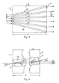
- the arrangement shown in FIG. 1 for fanning out light paths is structured as follows: On a base plate 3 there are six rectilinear strip waveguides 41 to 46. On the input side, six light paths with the mutual distance a 1 enter the arrangement. The input side edge of the base plate 3 is referred to as the input side 1. On the exit side 2, the six light paths with the distance a2 emerge again from the arrangement for fanning out.
- the optical axes of the incoming and outgoing light beams run parallel to one another and perpendicular to the input or output side 1, 2 of the base plate 3.
- the strip waveguides 41-46 are at the respective angles ⁇ i to the normal on the input and output side 1, 2 inclined.
- the angular relationships are shown in the detailed drawing in FIG. 2, which represents the start and end area of the strip waveguide 42.
- the strip waveguide 42 has two end faces 5 and 5 'which is inclined to the axis of the strip waveguide by the angle ⁇ i and to the normal on the input or output side 1, 2 by the angle ⁇ i .
- the angle of inclination ⁇ i results from the refractive index, so that the light beam on the input side after the refraction at the end face 5 runs exactly in the direction of the axis of the strip waveguide.
- the angular relationships on the input side and on the output side coincide with one another since it is a parallel offset.
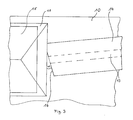
- FIG. 3 shows a top view of a silicon carrier 10 with an anisotropically etched V-groove 11 for receiving an optical fiber 15 or a round optic.
- the core layer has a higher refractive index than the buffer layer and the cladding layer.
- the waveguide consisting of core layer 13 and cladding layer 14 is structured on its end face 16 by reactive ion etching. The beveling with the angle ⁇ has not been carried out over the entire waveguide width, but only in the core area and on one side of the core. The distance between the waveguide and optical fiber 15 can thereby be reduced.
Landscapes
- Physics & Mathematics (AREA)
- General Physics & Mathematics (AREA)
- Optics & Photonics (AREA)
- Engineering & Computer Science (AREA)
- Microelectronics & Electronic Packaging (AREA)
- Optical Couplings Of Light Guides (AREA)
- Optical Integrated Circuits (AREA)
Abstract
Description
- Die Erfindung betrifft eine Anordnung zur Auffächerung von Lichtpfaden gemäß dem Oberbegriff des Patentanspruches 1.
- Beim Entwerfen optischer Module mit mehr als einem Lichtpfad tritt häufig das Problem auf, die Lichtpfade von einer ersten Funktionseinheit mit engen Lichtpfadabständen zu einer zweiten Funktionseinheit mit weiten Lichtpfadabständen zu führen, wobei die Abstände der Lichtpfade aufgefächert werden müssen. In den meisten Fällen müssen konstruktionsbedingt weitere Randbedingungen erfüllt sein: Die Lichtpfade müssen an den Koppelstellen parallel zueinander verlaufen und die Koppelstellen müssen in einer geraden Reihe liegen.
- Aus der US 4 878 724 ist es bekannnt, zur Auffächerung von Lichtpfaden zwei- oder mehrfach abgewinkelte gerade Lichtwellenleiter zu verwenden. Diese können sich auch schneiden. Eine solche Anordnung führt zu Abstrahlungsverlusten, die sich bei vielen Anwendungen negativ auswirken.
- Aus der EP 131 722 B1 ist es bekannt, zur Auffächerung der Lichtpfade gekrümmte Wellenleiter zu verwenden. Die Randbedingung, daß die Ein- und Austrittspfade parallel zueinander verlaufen müssen, wird nach dem Stand der Technik dadurch gelöst, daß für die Lichtpfade S-förmig gekrümmte Lichtwellenleiter verwendet werden. Wegen der Abstrahlverluste in gekrümmten Lichtwellenleitern darf der Krümmungsradius nicht zu klein sein. Will man einen vorgegebenen Parallelversatz der Lichtwellenleiter erreichen, so muß eine große Baulänge der Auffächerungseinheit gewählt werden. Beispielsweise bei einer Struktur, bei welcher der Lichtpfadabstand von 0 auf 125 Mikrometer zur Ankopplung zweier Fasern erweitert werden soll, beträgt die Länge der Auffächerungszone zwischen der Ein- und Austrittsseite jeweils ungefähr 10 mm und ist damit länger als die eigentliche Koppelzone. Sollen mehr als zwei Lichtpfade aufgefächert werden, so wächst der erforderliche Parallelversatz mit jedem Lichtpfad weiter an, was zu größerer Baulänge oder, bei stärkerer Krümmung der Wellenleiter, zu höheren Abstrahlverlusten führt.
- Ausgehend von diesem Stand der Technik ist es Aufgabe der Erfindung, eine Anordnung zur Auffächerung von Lichtpfaden anzugeben, die nur eine kleine Baulänge und geringe Abstrahlverluste aufweist.
- Die Aufgabe wird von einer Anordnung gemäß Anspruch 1 gelöst.
- Vorteilhafte Weiterbildungen sind in den Unteransprüchen angegeben.
- Die erfindungsgemäße Anordnung verwendet zwischen der ersten Funktionseinheit mit engen Lichtpfadabständen und der zweiten Funktionseinheit mit weiten Lichtpfadabständen gerade Lichtwellenleiter, die nahezu keine Abstrahlverluste aufweisen. Die erforderliche Lichtumlenkung erfolgt nicht durch Krümmung der Lichtpfade, sondern erfindungsgemäß durch Lichtbrechung an den Ein- und Austrittsflächen der Lichtwellenleiter der Anordnung. Die Lichtwellenleiter der Anordnung weisen dazu Ein- und Austrittsflächen auf, die zu einer auf der Lichtwellenleiterachse senkrechten Ebene geneigt verlaufen. Dies hat den Vorteil, daß Reflexionen nicht wieder in den Lichtpfad eingekoppelt werden und sich somit auch nicht störend auswirken können. Bei Verwendung von hochstabilen Lasern für die kohärente Übertragungstechnik ist dies besonders wichtig. Es genügt, wenn die Ein- und Austrittsflächen der Lichtwellenleiter jeweils im Kernbereich abgeschrägt sind. Dadurch kann der Abstand zwischen dem Lichtwellenleiter der Anordnung und den Funktionseinheiten in die ein- bzw. ausgekoppelt werden soll verringert werden.
- Um einen Parallelversatz zwischen den Funktioneinheiten und somit zwischen den eingangs- und ausgangsseitigen Lichtpfaden zu erreichen, muß die Anordnung zur Auffächerung eine zweimalige Lichtumlenkung vorsehen. Die Lichtpfade vor und hinter der Anordnung zur Auffächerung sind zueinander parallel, der Lichtpfad zwischen den Lichtumlenkungen ist gegen die Lichtpfade vor und hinter der Anordnung um den Winkel δi geneigt. Der Winkel δi ist für die verschiedenen Lichtpfade unterschiedlich. Er hängt davon ab, ob ein Lichtpfad bei einem Array zu den äußeren oder mittleren Lichtpfaden gehört. Ein Array ist meistens symmetrisch aufgebaut. Der Winkel δi ergibt sich für einen Lichtpfad jeweils aus dem Parallelversatz di und der Baulänge l für die Anordnung zur Auffächerung.

- Die Normalen auf den jeweiligen Stirnflächen der Lichtwellenleiter der Anordnung sind um einen Winkel αi gegen die Lichtpfade vor und hinter der Anordnung geneigt. Dadurch wird erreicht, daß das in die Lichtwellenleiter der Anordnung eingekoppelte Lichtbündel nach Brechung an der Stirnfläche auf der Lichtwellenleiterachse verläuft und daß das aus dem Lichtwellenleiter der Anordnung ausgekoppelte Lichtbündel nach Brechung wieder auf dem parallelen Lichtpfad verläuft. Die Normalen der Stirnflächen sind zur Achse des jeweiligen Lichtwellenleiters der Anordnung um den Winkel βi geneigt. Es gilt:

Für die Brechung gilt:

- Wobei n der Brechungsindex des Lichtwellenleiters ist. Für den Winkel αi ergibt sich:

- Da der Parallelversatz di für jeden Lichtpfad unterschiedlich ist, ist auch die Neigung der Stirnflächen für jeden Lichtpfad anders.
- Die Verwendung von einzelnen abgeschrägten Stirnflächen, wie sie für die erfindungsgemäße Anordnung notwendig ist, ist im Lichtwellenleiterarray normalerweise nicht üblich. Es bedeutet jedoch keinen Mehraufwand bei der Herstellung, wenn man beispielsweise Rippenwellenleiter verwendet, die auf fotolithografischem Wege strukturiert werden. Es müssen nur zusätzlich zu den Seitenkanten der Lichtwellenleiter auch noch die Stirnflächen erzeugt werden. Dies kann z.B. durch reaktives Ionenätzen geschehen.
- Besonders vorteilhaft ist eine Ausführung der erfindungsgemäßen Anordnung in Siliziumtechnik. Hier lassen sich durch anisotropes Ätzen Halterungsnuten für anzukoppelnde Faserarrays oder Mikrolinsenarrays herstellen. Auf dem gleichen Siliziumträger können beispielsweise durch Anwendung der Flammenhydrolyse aus SiCl₄-TiCl₄-Gemischen Wellenleiter aus SiO₂ mit TiO₂-Dotierung zur Anhebung des Brechungsindexes im Kernbereich hergestellt werden. Die Strukturierung der Seiten- und Stirnflächen der Rippenwellenleiter kann durch reaktives Ionenätzen über eine Fotoresistmaske erfolgen. Die erforderliche hohe Präzision für die Ankopplung wird dabei durch die Fotolithographie erreicht, so daß eine Justierung nicht mehr erforderlich ist.
- Die Anordnung zur Auffächerung von Lichtpfaden kann dann zwischen zwei Funktionseinheiten angebracht werden. Eine Funktionseinheit kann beispielsweise ein Richtkoppler, bei dem der Abstand zweier Lichtpfade wenige Mikrometer beträgt, eine Boastruktur, bei der die Lichtpfade direkt nebeneinander angeordnet sind, oder eine Laser oder Empfangsdiodenzeile mit einem Abstand der Lichtpfade von einigen zehn Mikrometern, sein. Auch ein Faserarray, bei dem die Lichtpfadabstände zumindest 125 Mikrometer betragen, oder eine Zeile mit mikrooptischen Abbildungskomponenten wie Kugellinsen, Selfoc-Linsen oder Hologrammen, können eine Funktionseinheit darstellen. Bei einer Zeile mit mikrooptischen Abbildungskomponenten sind deren gegenseitige Abstände mindestens so groß, wie die Durchmesser der Einzelkomponenten sein müssen. Diese liegen etwa bei 1 mm.
- Natürlich kann die Anordnung zur Auffächerung von Lichtpfaden in beiden Richtungen betrieben werden, d.h., das Licht kann sowohl auf der Seite eingekoppelt werden auf der die Lichtpfade weiter auseinander liegen als auch auf der Seite eingekoppelt werden auf der die Lichtpfade nahe nebeneinander liegen.
- Anhand der Figuren werden Ausführungsbeispiele der Erfindung erläutert. Es zeigen:
- Figur 1
- eine Anordnung zur Auffächerung von Lichtpfaden in der Draufsicht,
- Figur 2
- obige Anordnung in Detail und
- Figur 3
- eine Detailzeichnung einer Anordnung mit Streifenwellenleitern und Siliziumträger.
- Die in Figur 1 dargestellte Anordnung zur Auffächerung von Lichtpfaden ist wie folgt aufgebaut:
Auf einer Grundplatte 3 befinden sich sechs geradlinig verlaufende Streifenwellenleiter 41 bis 46. Eingangsseitig treten sechs Lichtpfade mit dem gegenseitigen Abstand a₁ in die Anordnung ein. Die eingangsseitige Kante der Grundplatte 3 wird als Eingangsseite 1 bezeichnet. Auf der Austrittsseite 2 treten die sechs Lichtpfade mit dem Abstand a₂ wieder aus der Anordnung zur Auffächerung aus. Die optischen Achsen der ein- und austretenden Lichtbündel verlaufen parallel zueinander und senkrecht zu der Eingangs- bzw. Austrittsseite 1, 2 der Grundplatte 3. Die Streifenwellenleiter 41-46 sind um die jeweiligen Winkel δi zur normalen auf der Eingangs- und Ausgangsseite 1, 2 geneigt. Die Winkelverhältnisse sind aus der Detailzeichnung in Figur 2 dargestellt, die den Anfangs- und Endbereich des Streifenwellenleiters 42 darstellt, ersichtlich. Der Winkel δi ergibt sich aus dem Auffächerungsversatz di und der Länge l der Grundplatte wie folgt:

- Der Streifenwellenleiter 42 weist zwei Stirnflächen 5 und 5' auf, die zur Achse des Streifenwellenleiters um den Winkel βi und zur Normalen auf der Eingangs- bzw. Ausgangsseite 1, 2 um den Winkel αi geneigt ist. Der Neigungswinkel αi ergibt sich aus dem Brechungsindex, damit das eingangsseitige Lichtbündel nach der Brechung an der Stirnfläche 5 genau in Richtung der Achse des Streifenwellenleiters verläuft. Die eingangsseitigen und ausgangsseitigen Winkelverhältnisse stimmen, da es sich um einen Parallelversatz handelt, miteinander überein. Figur 3 zeigt eine Draufsicht eines Siliziumträgers 10 mit anisotrop geätzter V-Nut 11 zur Aufnahme einer Lichtleitfaser 15 oder einer Rundoptik. Im Bereich der Auffächerung trägt der Siliziumträger eine Pfufferschicht, auf der eine Kernschicht 13 aufgebracht und strukturiert wurde. Diese ist umgeben von einer Mantelschicht 14. Die Kernschicht hat einen höheren Brechungsindex als die Pfufferschicht und die Mantelschicht. Durch reaktives Ionenätzen wird der aus Kernschicht 13 und Mantelschicht 14 bestehende Wellenleiter an seiner Stirnfläche 16 strukturiert. Die Abschrägung mit dem Winkel α ist hierbei nicht über die gesamte Wellenleiterbreite durchgeführt worden, sondern nur im Kernbereich und auf einer Seite des Kernes erfolgt. Dadurch kann der Abstand zwischen Wellenleiter und Lichtleitfaser 15 verringert werden.
Claims (9)
- Anordnung zur Auffächerung von Lichtpaden, die eine Grundplatte (3) mit einer Eingangs- und einer Austrittsseite (1, 2) aufweist, auf der mindestens zwei Lichtwellenleiter (41-46) aufgebracht sind, die jeweils einen Lichtpfad im Eingangsbereich mit einem Lichtpfad im Austrittsbereich verbinden, wobei die Lichtpfade im Eingangs- und Austrittsbereich zueinander parallel verlaufen, der Abstand der Lichtpfade im Eingangsbereich sich vom Abstand der Lichtpfade im Austrittsbereich unterscheidet und die Normalen auf der Eingangs- und Austrittsseite (1, 2) parallel zu den Lichtpfaden im Eingangs- und Austrittsbereich verlaufen, dadurch gekennzeichnet, daß alle Lichtwellenleiter (41-46) durchgehend auf der gesamten Strecke zwischen dem Eingangs- und Austrittsbereich als Geraden verlaufen, wobei sich die Geraden nicht schneiden, daß die Lichtwellenleiter (41-46) Stirnflächen (5, 5') aufweisen, die derart ausgestaltet sind, daß beim Ein- oder Auskoppeln von Licht in oder - aus dem Lichtwellenleiter (41-46), dieses Licht derart gebrochen wird, daß es nach dem Einkoppeln auf der Achse des Lichtwellenleiter (41-46) und nach dem Auskoppeln wieder in Richtung der parallelen austrittsseitigen Lichtpfade verläuft.
- Anordnung zur Auffächerung von Lichtpfaden nach Anspruch 1, dadurch gekennzeichnet, daß die Stirnflächen (5, 5') zumindest bereichsweise und zumindest im Kernbereich des Lichtwellenleiters (41-46) gegen die Achse des jeweiligen Lichtwellenleiters (41-46) geneigt sind.
- Anordnung zur Auffächerung von Lichtpfaden nach Anspruch 2, dadurch gekennzeichnet, daß der Neigungswinkel αi, zwischen der Normalen auf der Stirnfläche (5, 5') und der Normalen auf der Eingangs- und Austrittsseite (1, 2), sich wie folgt ergibt:

wobei n der Brechungsindex des Lichtwellenleiters und δi der Winkel zwischen der Richtung der parallen ein- und austrittsseitigen Lichtpfade und der Achse des jeweiligen Lichtwellenleiters (41-46) ist. - Anordnung zur Auffächerung von Lichtpfaden nach einem der Ansprüche 1 bis 3, dadurch gekennzeichnet, daß die Lichtwellenleiter 41-46) Streifenleiter sind.
- Anordnung zur Auffächerung von Lichtpfaden nach einem der Ansprüche 1 bis 3, dadurch gekennzeichnet, daß die Lichtwellenleiter (41-46) Lichtleitfasern sind, die auf der Grundplatte (3) aufgebracht werden.
- Anordnung zur Auffächerung von Lichtpfaden nach einem der Ansprüche 1 bis 5, dadurch gekennzeichnet, daß die Grundplatte (3) ein Siliziumträger (10) ist.
- Anordnung zur Auffächerung von Lichtpfaden nach Anspruch 6, dadurch gekennzeichnet, daß in dem Siliziumträger (10) anisotrop geätzte V-Nuten (11) vorgesehen sind, die zur Aufnahme von Lichtleitfasern dienen.
- Anordnung zur Auffächerung von Lichtpfaden nach einem der bisherigen Ansprüche, dadurch gekennzeichnet, daß die Grundplatte (3) derart ausgestaltet ist, daß eingangsseitig und ausgangsseitig Funktionseinheiten mit parallelen Lichtpfaden anbringbar sind.
- Anordnung zur Auffächerung von Lichtpfaden nach Anspruch 8, dadurch gekennzeichnet, daß sich die Funktionseinheiten an der Grundplatte (3) an die Eingangs- und Austrittsseite (1,2) direkt anschließen.
Applications Claiming Priority (2)
| Application Number | Priority Date | Filing Date | Title |
|---|---|---|---|
| DE19904009323 DE4009323C1 (de) | 1990-03-23 | 1990-03-23 | |
| DE4009323 | 1990-03-23 |
Publications (2)
| Publication Number | Publication Date |
|---|---|
| EP0447639A1 true EP0447639A1 (de) | 1991-09-25 |
| EP0447639B1 EP0447639B1 (de) | 1994-05-04 |
Family
ID=6402877
Family Applications (1)
| Application Number | Title | Priority Date | Filing Date |
|---|---|---|---|
| EP19900124042 Expired - Lifetime EP0447639B1 (de) | 1990-03-23 | 1990-12-13 | Anordnung zur Auffächerung von Lichtpfaden |
Country Status (2)
| Country | Link |
|---|---|
| EP (1) | EP0447639B1 (de) |
| DE (1) | DE4009323C1 (de) |
Cited By (1)
| Publication number | Priority date | Publication date | Assignee | Title |
|---|---|---|---|---|
| CN118311710A (zh) * | 2024-04-30 | 2024-07-09 | 中国电子科技集团有限公司电子科学研究院 | 一种扇形光纤波导阵列模块 |
Families Citing this family (4)
| Publication number | Priority date | Publication date | Assignee | Title |
|---|---|---|---|---|
| ATE127249T1 (de) * | 1991-12-21 | 1995-09-15 | Hal Sicherheitstechnik Gmbh | Einrichtung zum überwachen eines verschlusses. |
| DE19742895C2 (de) * | 1997-09-24 | 1999-10-21 | Siemens Ag | Elektrooptische Anordnung |
| US6049641A (en) * | 1998-02-24 | 2000-04-11 | Gemfire Corporation | Connection system for optical redundancy |
| CN110426787B (zh) * | 2019-07-04 | 2020-12-22 | 苏州安捷讯光电科技股份有限公司 | 一种带衰减非接触式光纤回路器及其制作方法 |
Citations (3)
| Publication number | Priority date | Publication date | Assignee | Title |
|---|---|---|---|---|
| US4094579A (en) * | 1976-09-13 | 1978-06-13 | Sperry Rand Corporation | Multimode optical waveguide device with non-normal butt coupling of fiber to electro-optic planar waveguide |
| US4523803A (en) * | 1981-02-27 | 1985-06-18 | Canon Kabushiki Kaisha | Optical scanning device |
| DD279751A1 (de) * | 1986-07-31 | 1990-06-13 | Univ Schiller Jena | Verfahren zur herstellung eines wellenleiterkopplers |
Family Cites Families (2)
| Publication number | Priority date | Publication date | Assignee | Title |
|---|---|---|---|---|
| FR2547071B1 (fr) * | 1983-05-31 | 1986-02-14 | Cit Alcatel | Dispositif opto-electronique de commutation spatiale |
| US4878724A (en) * | 1987-07-30 | 1989-11-07 | Trw Inc. | Electrooptically tunable phase-locked laser array |
-
1990
- 1990-03-23 DE DE19904009323 patent/DE4009323C1/de not_active Expired - Lifetime
- 1990-12-13 EP EP19900124042 patent/EP0447639B1/de not_active Expired - Lifetime
Patent Citations (3)
| Publication number | Priority date | Publication date | Assignee | Title |
|---|---|---|---|---|
| US4094579A (en) * | 1976-09-13 | 1978-06-13 | Sperry Rand Corporation | Multimode optical waveguide device with non-normal butt coupling of fiber to electro-optic planar waveguide |
| US4523803A (en) * | 1981-02-27 | 1985-06-18 | Canon Kabushiki Kaisha | Optical scanning device |
| DD279751A1 (de) * | 1986-07-31 | 1990-06-13 | Univ Schiller Jena | Verfahren zur herstellung eines wellenleiterkopplers |
Non-Patent Citations (3)
| Title |
|---|
| JOURNAL OF LIGHTWAVE TECHNOLOGY Band LT-3, Nr. 5, Oktober 1985, Seiten 1159-1162, New York, US; J. LIPSON et al.: "A six-channel wavelength multiplexer and demultiplexer for single mode systems" * |
| OPTICS LETTERS Band 13, Nr. 5, Mai 1988, Seiten 425-427, New York, NY, US; B.E. KINCAID: "Coupling of polarization-maintaining optical fibers to Ti:LiNbO3 waveguides with angled interfaces" * |
| PATENT ABSTRACTS OF JAPAN Band 12, Nr. 173 (P-706), 24. Mai 1988; & JP - A - 62283301 (ASAHI GLASS) 09.12.1987 * |
Cited By (1)
| Publication number | Priority date | Publication date | Assignee | Title |
|---|---|---|---|---|
| CN118311710A (zh) * | 2024-04-30 | 2024-07-09 | 中国电子科技集团有限公司电子科学研究院 | 一种扇形光纤波导阵列模块 |
Also Published As
| Publication number | Publication date |
|---|---|
| EP0447639B1 (de) | 1994-05-04 |
| DE4009323C1 (de) | 1991-02-21 |
Similar Documents
| Publication | Publication Date | Title |
|---|---|---|
| DE69522051T2 (de) | Anamorphotische Microlinse zum Einkoppeln elliptischer Lichtstrahlen in optische Fasern | |
| DE69316878T2 (de) | Optischer faser-laser und zugehöriger optischer koppler | |
| DE69618087T2 (de) | Mechanischer faseroptischer Schalter | |
| DE60110901T2 (de) | Faserkoppler, system und zugehörige verfahren zur reduktion von rückreflektionen | |
| DE3751674T2 (de) | Optischer Faserkoppler | |
| DE69727270T2 (de) | Verfahren zur Herstellung und Montage von einem kollektiven optischen Kopplungselement am Ende eines Bündels von mehreren Monomodenfasern | |
| DE60214186T2 (de) | Verfahren zur Herstellung von optischen Faserkollimatoren im Array | |
| DE2745940A1 (de) | Optisches schaltkreiselement | |
| DE3854441T2 (de) | Faseroptischer Abzweiger unter Verwendung eines Reflektors. | |
| DE68914349T2 (de) | Methode zur Herstellung eines optischen Verzweigungs- und Kopplungselements. | |
| EP0735397A2 (de) | Mikrooptische Vorrichtung zum Umformen von Strahlenbündeln einer Laserdiodenanordnung sowie Verfahren zur Herstellung dieser Vorrichtung | |
| DE2428570C2 (de) | Anordnung zur optischen Signalübertragung | |
| DE19510559C1 (de) | Optische Sende- und Empfangsanordnung | |
| DE2905916A1 (de) | Faseroptische uebertragungsvorrichtung | |
| US4247165A (en) | Fiber optic plate | |
| EP0923749B1 (de) | Lichtübertragungsvorrichtung | |
| DE4009323C1 (de) | ||
| DE69923883T2 (de) | 2 x 2 Faseroptischer Schalter | |
| DE19613755A1 (de) | Optisches Koppelelement | |
| EP0667545B1 (de) | Anordnung zur Anpassung unterschiedlicher Feldverteilungen von Lichtstrahlen | |
| DE3788664T2 (de) | Optische Leiter. | |
| EP0568851A2 (de) | Optische Sende- und Empfangsanordnung | |
| EP0453655B1 (de) | Lichtmischer | |
| DE4240460C2 (de) | Vorrichtung zur lösbaren Verbindung von Lichtwellenleitern | |
| EP2483724B1 (de) | Leiterplatte für optische und/oder elektronische bauteile |
Legal Events
| Date | Code | Title | Description |
|---|---|---|---|
| PUAI | Public reference made under article 153(3) epc to a published international application that has entered the european phase |
Free format text: ORIGINAL CODE: 0009012 |
|
| 17P | Request for examination filed |
Effective date: 19901228 |
|
| AK | Designated contracting states |
Kind code of ref document: A1 Designated state(s): FR GB IT NL SE |
|
| 17Q | First examination report despatched |
Effective date: 19930304 |
|
| GRAA | (expected) grant |
Free format text: ORIGINAL CODE: 0009210 |
|
| ITF | It: translation for a ep patent filed | ||
| AK | Designated contracting states |
Kind code of ref document: B1 Designated state(s): FR GB IT NL SE |
|
| ET | Fr: translation filed | ||
| GBT | Gb: translation of ep patent filed (gb section 77(6)(a)/1977) |
Effective date: 19940811 |
|
| EAL | Se: european patent in force in sweden |
Ref document number: 90124042.4 |
|
| PLBE | No opposition filed within time limit |
Free format text: ORIGINAL CODE: 0009261 |
|
| STAA | Information on the status of an ep patent application or granted ep patent |
Free format text: STATUS: NO OPPOSITION FILED WITHIN TIME LIMIT |
|
| 26N | No opposition filed | ||
| PGFP | Annual fee paid to national office [announced via postgrant information from national office to epo] |
Ref country code: NL Payment date: 19961223 Year of fee payment: 7 |
|
| PGFP | Annual fee paid to national office [announced via postgrant information from national office to epo] |
Ref country code: GB Payment date: 19971127 Year of fee payment: 8 |
|
| PGFP | Annual fee paid to national office [announced via postgrant information from national office to epo] |
Ref country code: FR Payment date: 19971218 Year of fee payment: 8 |
|
| PGFP | Annual fee paid to national office [announced via postgrant information from national office to epo] |
Ref country code: SE Payment date: 19971219 Year of fee payment: 8 |
|
| PG25 | Lapsed in a contracting state [announced via postgrant information from national office to epo] |
Ref country code: NL Free format text: LAPSE BECAUSE OF NON-PAYMENT OF DUE FEES Effective date: 19980701 |
|
| NLV4 | Nl: lapsed or anulled due to non-payment of the annual fee |
Effective date: 19980701 |
|
| PG25 | Lapsed in a contracting state [announced via postgrant information from national office to epo] |
Ref country code: GB Free format text: LAPSE BECAUSE OF NON-PAYMENT OF DUE FEES Effective date: 19981213 |
|
| PG25 | Lapsed in a contracting state [announced via postgrant information from national office to epo] |
Ref country code: SE Free format text: LAPSE BECAUSE OF NON-PAYMENT OF DUE FEES Effective date: 19981214 |
|
| GBPC | Gb: european patent ceased through non-payment of renewal fee |
Effective date: 19981213 |
|
| PG25 | Lapsed in a contracting state [announced via postgrant information from national office to epo] |
Ref country code: FR Free format text: LAPSE BECAUSE OF NON-PAYMENT OF DUE FEES Effective date: 19990831 |
|
| REG | Reference to a national code |
Ref country code: FR Ref legal event code: ST |
|
| PG25 | Lapsed in a contracting state [announced via postgrant information from national office to epo] |
Ref country code: IT Free format text: LAPSE BECAUSE OF NON-PAYMENT OF DUE FEES;WARNING: LAPSES OF ITALIAN PATENTS WITH EFFECTIVE DATE BEFORE 2007 MAY HAVE OCCURRED AT ANY TIME BEFORE 2007. THE CORRECT EFFECTIVE DATE MAY BE DIFFERENT FROM THE ONE RECORDED. Effective date: 20051213 |