EP0447798A2 - Test apparatus for printed circuits with IC's on both sides - Google Patents
Test apparatus for printed circuits with IC's on both sides Download PDFInfo
- Publication number
- EP0447798A2 EP0447798A2 EP91102076A EP91102076A EP0447798A2 EP 0447798 A2 EP0447798 A2 EP 0447798A2 EP 91102076 A EP91102076 A EP 91102076A EP 91102076 A EP91102076 A EP 91102076A EP 0447798 A2 EP0447798 A2 EP 0447798A2
- Authority
- EP
- European Patent Office
- Prior art keywords
- circuit board
- printed circuit
- measuring head
- sides
- contact pins
- Prior art date
- Legal status (The legal status is an assumption and is not a legal conclusion. Google has not performed a legal analysis and makes no representation as to the accuracy of the status listed.)
- Granted
Links
Images
Classifications
-
- G—PHYSICS
- G01—MEASURING; TESTING
- G01R—MEASURING ELECTRIC VARIABLES; MEASURING MAGNETIC VARIABLES
- G01R1/00—Details of instruments or arrangements of the types included in groups G01R5/00 - G01R13/00 and G01R31/00
- G01R1/02—General constructional details
- G01R1/06—Measuring leads; Measuring probes
- G01R1/067—Measuring probes
- G01R1/073—Multiple probes
- G01R1/07307—Multiple probes with individual probe elements, e.g. needles, cantilever beams or bump contacts, fixed in relation to each other, e.g. bed of nails fixture or probe card
- G01R1/07314—Multiple probes with individual probe elements, e.g. needles, cantilever beams or bump contacts, fixed in relation to each other, e.g. bed of nails fixture or probe card the body of the probe being perpendicular to test object, e.g. bed of nails or probe with bump contacts on a rigid support
- G01R1/07328—Multiple probes with individual probe elements, e.g. needles, cantilever beams or bump contacts, fixed in relation to each other, e.g. bed of nails fixture or probe card the body of the probe being perpendicular to test object, e.g. bed of nails or probe with bump contacts on a rigid support for testing printed circuit boards
- G01R1/07335—Multiple probes with individual probe elements, e.g. needles, cantilever beams or bump contacts, fixed in relation to each other, e.g. bed of nails fixture or probe card the body of the probe being perpendicular to test object, e.g. bed of nails or probe with bump contacts on a rigid support for testing printed circuit boards for double-sided contacting or for testing boards with surface-mounted devices (SMD's)
Definitions
- the invention relates to a test device for printed circuit boards equipped with integrated circuits on both sides, consisting of a holder for a printed circuit board and a measuring head having a plurality of contact pins, which can be lowered onto the printed circuit board, and a positioning device for the relative position of the measuring head and printed circuit board.
- the holder for the printed circuit board is cup-shaped and supports the printed circuit board at its edge. As long as the circuit board only contains complete circuits on each side, the individual circuits can be checked one after the other without any problems. If one side of the circuit board is checked, the circuits on the other side are checked after turning the circuit board. However, the test becomes problematic when a circuit is composed of parts located on both sides of the printed circuit boards.
- the invention has for its object to provide a test device for printed circuit boards equipped with integrated circuits on both sides, in which the device-related expenditure is lower than in the known test device.
- the holder consists of a base and arranged on it, the circuit board only grasping the edge and holding it with a free working space above the base, that there is another under the one measuring head is positioned on the circuit board lowerable measuring head, which has the contact pins of a measuring head facing contact pins and that the two measuring heads, which are floating on a support by means of flexible stops in the lowering direction, can be adjusted in their mutual distance by means of an actuator.
- the circuit board can be positioned between the pair of measuring heads with respect to the individual circuits to be tested and the measuring heads can be placed on the circuit to be tested with their contact pins in the manner of pliers.
- the one with it The associated load on the circuit board, in particular the circuit board which is sensitive to breakage in the case of a ceramic version, is low because the pair of measuring heads adjusts itself automatically to the position of the circuit board because of the floating mounting and the coupling of the measuring heads via the actuator.
- the flexible stop for the upper measuring head intercepts its weight and, after the actuator has responded, also the weight of the lower measuring head, so that the contact pins are placed on the circuit board and the required contact pressure is applied practically without one-sided loading.
- the actuator is an actuating cylinder which is effective between the measuring heads. Since the exact position of the circuit board is predetermined by the holding elements, the end position of the measuring heads can also be predetermined, so that it is not necessary to set the contact pressure via the actuator. According to a further embodiment of the invention, this can be achieved in that each measuring head is assigned a fixed stop effective in the lowering direction.
- the positioning device is preferably designed as a cross table which can be moved in two mutually perpendicular axes and forms the base. Basically, it is also possible to make the required relative movement between the pair of measuring heads and the circuit board by moving the measuring heads together, but since these are already being raised and lowered, the relative movement in the plane of the circuit board can be achieved more easily by the movement of the circuit board.
- a base 2 designed as a cross table can be moved horizontally in two mutually perpendicular axes.
- the base 2 carries on rods 3, 4, 5 two pairs of wedge rollers 6, 7, 8, of which the two pairs are arranged at a right angle.
- a tension member 9 is assigned to these wedge rollers 6, 7, 8.
- the wedge rollers 6 to 8 and the tension member 9 form holding elements for a printed circuit board 10 equipped on both sides with a large number of integrated circuits the tendon 9 acting on the diagonal point is kept aligned.
- a support column 11 is arranged on the base plate 1, in which two arms 13, 14 are slidably mounted in a vertical guide 12.
- the arms 13, 14 carry measuring heads 15, 16 at their free ends, each of which is equipped with contact pins 17, 18 facing one another.
- One measuring head 15 is located above the circuit board 10 and the other in the free working space located under the circuit board 10.
- the lower arm 14 is supported on an adjustable stop 19, so that the contact pins 18 are at a sufficiently large distance from the circuit board 10 in order to be able to move the circuit board 10 without hindrance.
- the upper arm 13 is held in the position shown in the drawing by an actuator 20 designed as a double-acting cylinder piston arrangement, which between the both arms 13, 14 is effective.
- Both the upper arm 13 and the lower arm 14 each have a resilient stop 21, 22 acting as a damping member and an adjustable, fixed stop 23, 24. These stops 21 to 24 cooperate with a support element 25 carried by the column 1.
- the test device works as follows: After the circuit board 10 is positioned and clamped by the holding elements 6 to 8 and the clamping element 9, the cross table with its base 2 is moved so that the circuit board 10 is located between the upper and lower measuring heads 15, 16, as shown in the drawing is. After the cross table has positioned the circuit board 10 with respect to a circuit relative to the measuring heads 15, 16, the actuator 20 is relieved of pressure, so that the arm 13 with the measuring head 15 lowers due to its own weight until the flexible stop 21 is supported by the support 25 is able to carry the arm 13. In this position, the contact pins 17 have not yet touched the circuit board. The actuator 20 is then pressurized, as a result of which the arm 14 lifts off the stop 19 and the flexible stop 22 comes to rest on the support 25.
- the resilient stop 21 Since after lifting the lower arm 14 from the stop 19, the lower arm is suspended from the actuator 20 on the upper arm 13, the resilient stop 21 must absorb the total weight of the two arms 13, 14 and the measuring heads 15, 16. Therefore, its pretension should be set so that it can carry the entire weight without touching the contact pins 17. If the actuator 20 is pressurized continuously, the lower resilient stop 22 also comes to rest on the support 25. The prestressing of this resilient stop 22 is open the bias of the upper resilient stop 21 adjusted so that there is a practically floating mounting of the two arms 13, 14 in the vertical direction. Therefore, the contact pins 17, 18 put on the pressure of the actuator 20 practically without force on the circuits of the circuit board 10, without the circuit board 10 being loaded on one side or the other by pressure.
- the measuring heads 15, 18 are moved apart again by applying pressure to the actuating element 20, which can be acted on from both sides, and the circuit board 10 is brought into a different position relative to the measuring heads 15, 16 by means of the cross table 2. The process described is then repeated.
- the tester is suitable for the printed circuit board with integrated circuits on both sides, in which the parts on opposite sides either form a single circuit or two independent circuits.
Landscapes
- Physics & Mathematics (AREA)
- General Physics & Mathematics (AREA)
- Tests Of Electronic Circuits (AREA)
- Testing Of Short-Circuits, Discontinuities, Leakage, Or Incorrect Line Connections (AREA)
- Structure Of Printed Boards (AREA)
- Production Of Multi-Layered Print Wiring Board (AREA)
Abstract
Die Erfindung bezieht sich auf ein Prüfgerät für beidseitig mit integrierten Schaltungen bestückte Leiterplatten 10. Zur gleichzeitigen Prüfung von auf gegenüberliegenden Seiten der Leiterplatte 10 angeordnete Schaltungen sind auf beiden Seiten der Leiterplatte 10 mit Kontaktstiften 17, 18 bestückte Meßköpfe 16, 17 vorgesehen, die auf die Leiterplatte 10 absenkbar sind. Beide Meßköpfe 15, 16 sind gemeinsam schwimmend in Absenkrichtung an einem Träger 11 gelagert, so daß beim Absenken der Meßköpfe 15, 16 deren Eigengewicht nicht einseitig die Leiterplatte 10 belastet sondern die Kontaktdrücke beider Meßköpfe 15, 16 an der Leiterplatte 10 sich gegenseitig aufheben. Dadurch wird ein gleichzeitiges Prüfen der Schaltungen beider Seiten der Leiterplatte 10 ermöglicht, ohne daß dabei die Leiterplatte 10 durch einseitige Belastung bruchgefährdet wird.
Description
Die Erfindung bezieht sich auf ein Prüfgerät für beidseitig mit integrierten Schaltungen bestückte Leiterplatten, bestehend aus einem Halter für eine Leiterplatte und einem eine Vielzahl von Kontaktstiften aufweisenden, auf die Leiterplatte absenkbaren Meßkopf sowie einer Positioniereinrichtung für die relative Lage von Meßkopf und Leiterplatte.The invention relates to a test device for printed circuit boards equipped with integrated circuits on both sides, consisting of a holder for a printed circuit board and a measuring head having a plurality of contact pins, which can be lowered onto the printed circuit board, and a positioning device for the relative position of the measuring head and printed circuit board.
Bei einem aus der Praxis bekannten Prüfgerät dieser Art ist der Halter für die Leiterplatte schalenförmig ausgebildet und stützt die Leiterplatte an ihrem Rand ab. Solange die Leiterplatte auf jeder Seite nur komplette Schaltungen umfaßt, lassen sich die einzelnen Schaltungen nacheinander problemlos prüfen. Ist die eine Seite der Leiterplatte geprüft, erfolgt nach Wenden der Leiterplatte die Prüfung der Schaltungen der anderen Seite. Problematisch wird die Prüfung aber dann, wenn sich eine Schaltung aus auf beiden Seiten der Leiterplatten befindlichen Teilen zusammensetzt.In a test device of this type known from practice, the holder for the printed circuit board is cup-shaped and supports the printed circuit board at its edge. As long as the circuit board only contains complete circuits on each side, the individual circuits can be checked one after the other without any problems. If one side of the circuit board is checked, the circuits on the other side are checked after turning the circuit board. However, the test becomes problematic when a circuit is composed of parts located on both sides of the printed circuit boards.
In diesem Fall läßt sich eine Schaltung nur prüfen, wenn sie gleichzeitig auf beiden Seiten kontaktiert werden kann. Dieses Problem hat man in der Weise gelöst, daß der schalenförmige Halter für jeden von ihm abgedeckten Schaltungsteil der auf der Leiterplatte befindlichen Schaltungen mit Kontaktstiften bestückt ist, die die erforderlichen Kontaktbrücken für die Prüfung bei auf der frei zugänglichen Seite aufgesetztem Meßkopf bilden. Ein solches Prüfgerät ist wegen der vielen Sätze von Kontaktstiften für die verdeckten Schaltungsteile aufwendig.In this case, a circuit can only be checked if it can be contacted on both sides at the same time. This problem has been solved in such a way that the cup-shaped holder is equipped with contact pins for each of the circuit parts of the circuits on the circuit board that it covers, which form the necessary contact bridges for testing with the measuring head attached to the freely accessible side. Such a test device is complex because of the many sets of contact pins for the hidden circuit parts.
Der Erfindung liegt die Aufgabe zugrunde, ein Prüfgerät für beidseitig mit integrierten Schaltungen bestückte Leiterplatten zu schaffen, bei dem der gerätetechnische Aufwand geringer als bei dem bekannten Prüfgerät ist.The invention has for its object to provide a test device for printed circuit boards equipped with integrated circuits on both sides, in which the device-related expenditure is lower than in the known test device.
Diese Aufgabe wird erfindungsgemäß bei einem Prüfgerät der eingangs genannten Art dadurch gelöst, daß der Halter aus einem Sockel und darauf angeordneten, die Leiterplatte nur am Rand erfassenden und sie mit einem freien Arbeitsraum über dem Sockel haltenden Halteelementen besteht, daß unter dem einen Meßkopf ein weiterer auf die Leiterplatte absenkbarer Meßkopf positioniert ist, der den Kontaktstiften des einen Meßkopfes zugewandte Kontaktstifte aufweist und daß die beiden Meßköpfe, die an einem Träger mittels nachgiebiger Anschläge in Absenkrichtung schwimmend gelagert sind, in ihrem gegenseitigen Abstand mittels eines Stellgliedes einstellbar sind.This object is achieved in a test device of the type mentioned above in that the holder consists of a base and arranged on it, the circuit board only grasping the edge and holding it with a free working space above the base, that there is another under the one measuring head is positioned on the circuit board lowerable measuring head, which has the contact pins of a measuring head facing contact pins and that the two measuring heads, which are floating on a support by means of flexible stops in the lowering direction, can be adjusted in their mutual distance by means of an actuator.
Bei dem erfindungsgemäßen Prüfgerät läßt sich die Leiterplatte bezüglich der einzelnen zu prüfenden Schaltungen zwischen dem Meßkopfpaar positionieren und die Meßköpfe lassen sich mit ihren Kontaktstiften zangenartig auf die zu prüfende Schaltung aufsetzen. Die damit verbundene Belastung der Leiterplatte, insbesondere der bei einer Ausführung in Keramik bruchempfindlichen Leiterplatte ist gering, weil wegen der schwimmenden Lagerung und der Kupplung der Meßköpfe über das Stellglied sich das Meßkopfpaar auf die Lage der Leiterplatte selbständig einstellt. So fängt der nachgiebige Anschlag für den oberen Meßkopf dessen Gewicht und, nachdem das Stellglied angesprochen hat, auch das Gewicht des unteren Meßkopfes ab, so daß praktisch ohne einseitige Belastung die Kontaktstifte auf die Leiterplatte aufsetzen und den erforderlichen Kontaktdruck aufbringen.In the test device according to the invention, the circuit board can be positioned between the pair of measuring heads with respect to the individual circuits to be tested and the measuring heads can be placed on the circuit to be tested with their contact pins in the manner of pliers. The one with it The associated load on the circuit board, in particular the circuit board which is sensitive to breakage in the case of a ceramic version, is low because the pair of measuring heads adjusts itself automatically to the position of the circuit board because of the floating mounting and the coupling of the measuring heads via the actuator. The flexible stop for the upper measuring head intercepts its weight and, after the actuator has responded, also the weight of the lower measuring head, so that the contact pins are placed on the circuit board and the required contact pressure is applied practically without one-sided loading.
Nach einer Ausgestaltung der Erfindung ist das Stellglied ein zwischen den Meßköpfen wirksamer Stellzylinder. Da die genaue Position der Leiterplatte durch die Halteelemente vorgegeben ist, läßt sich auch die Endposition der Meßköpfe vorgeben, so daß es nicht erforderlich ist, über das Stellglied den Kontaktdruck einzustellen. Dies läßt sich nach einer weiteren Ausgestaltung der Erfindung dadurch verwirklichen, daß jedem Meßkopf ein in Absenkrichtung wirksamer fester Anschlag zugeordnet ist.According to one embodiment of the invention, the actuator is an actuating cylinder which is effective between the measuring heads. Since the exact position of the circuit board is predetermined by the holding elements, the end position of the measuring heads can also be predetermined, so that it is not necessary to set the contact pressure via the actuator. According to a further embodiment of the invention, this can be achieved in that each measuring head is assigned a fixed stop effective in the lowering direction.
Um das Meßkopfpaar gegenüber den einzelnen Schaltungen auf der Leiterplatte zu positionieren, ist vorzugsweise die Positioniereinrichtung als ein in zwei zueinander senkrechten Achsen verfahrbarer, den Sockel bildender Kreuztisch ausgebildet. Grundsätzlich ist es zwar auch möglich, die erforderliche Relativbewegung zwischen dem Meßkopfpaar und der Leiterplatte durch gemeinsames Verfahren der Meßköpfe vorzunehmen, doch da diese schon angehoben und abgesenkt werden, läßt sich die Relativbewegung in der Ebene der Leiterplatte leichter durch die Bewegung der Leiterplatte erreichen.In order to position the pair of measuring heads relative to the individual circuits on the printed circuit board, the positioning device is preferably designed as a cross table which can be moved in two mutually perpendicular axes and forms the base. Basically, it is also possible to make the required relative movement between the pair of measuring heads and the circuit board by moving the measuring heads together, but since these are already being raised and lowered, the relative movement in the plane of the circuit board can be achieved more easily by the movement of the circuit board.
Im folgenden wird die Erfindung anhand eines ein Ausführungsbeispiel schematisch in Seitenansicht darstellenden Prüfgerätes erläutert.In the following the invention is based on a Exemplary embodiment schematically explained in a side view of the test device.
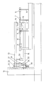
Auf einer Grundplatte 1 ist ein als Kreuztisch ausgebildeter Sockel 2 in der Horizontalen in zwei zueinander senkrechten Achsen verfahrbar. Der Sockel 2 trägt auf Stäben 3,4,5 zwei Paar Keilrollen 6,7,8, von denen die beiden Paare unter einem rechten Winkel angeordnet sind. Diesen Keilrollen 6,7,8 ist ein Spannglied 9 zugeordnet. Die Keilrollen 6 bis 8 und das Spannglied 9 bilden Halteelemente für eine auf beiden Seiten mit einer Vielzahl von integrierten Schaltungen bestückte Leiterplatte 10. Die Leiterplatte 10 liegt mit zwei unter einem rechten Winkel angeordneten Rändern an den Keilrollen 6 und 7 beziehungsweise 8 an und wird durch das an der Diagonalen liegenden Spitze angreifende Spannglied 9 ausgerichtet gehalten.On a base plate 1, a base 2 designed as a cross table can be moved horizontally in two mutually perpendicular axes. The base 2 carries on
Auf der Bodenplatte 1 ist eine Tragsäule 11 angeordnet, bei der in einer vertikalen Führung 12 zwei Arme 13,14 verschieblich gelagert sind. Die Arme 13,14 tragen an ihren freien Enden Meßköpfe 15,16, die jeweils mit aufeinander zugerichteten Kontaktstiften 17,18 bestückt sind. Der eine Meßkopf 15 befindet sich oberhalb der Leiterplatte 10 und der andere in dem unter der Leiterplatte 10 befindlichen freien Arbeitsraum.A
In der in der Zeichnung befindlichen Position ist der untere Arm 14 an einem einstellbaren Anschlag 19 abgestützt, so daß die Kontaktstifte 18 einen ausreichend großen Abstand von der Leiterplatte 10 haben, um die Leiterplatte 10 ohne Behinderung verfahren zu können. Der obere Arm 13 wird in der in der Zeichnung dargestellten Position durch ein als doppelseitig beaufschlagbare Zylinderkolbenanordnung ausgebildetes Stellglied 20 gehalten, das zwischen den beiden Armen 13,14 wirksam ist. Sowohl der obere Arm 13 als auch der untere Arm 14 haben jeweils einen nachgiebigen, als Dämpfungsglied wirkenden Anschlag 21,22 und einen einstellbaren festen Anschlag 23,24. Diese Anschläge 21 bis 24 wirken mit einem von der Säule 1 getragenen Stützelement 25 zusammen.In the position shown in the drawing, the
Die Arbeitsweise des Prüfgerätes ist folgende:
Nachdem die Leiterplatte 10 von den Halteelementen 6 bis 8 und dem Spannelement 9 positioniert und eingespannt ist, wird der Kreuztisch mit seinem Sockel 2 verfahren, so daß sich die Leiterplatte 10 zwischen dem oberen und unteren Meßkopf 15,16 befindet, wie in der Zeichnung dargestellt ist. Nachdem der Kreuztisch die Leiterplatte 10 bezüglich einer Schaltung gegenüber den Meßköpfen 15,16 positioniert hat, wird das Stellglied 20 druckentlastet, so daß der Arm 13 mit dem Meßkopf 15 sich aufgrund seines Eigengewichtes absenkt, bis daß der nachgiebige Anschlag 21 durch Abstützung an der Stütze 25 den Arm 13 zu tragen imstande ist. In dieser Position haben die Kontaktstifte 17 die Leiterplatte noch nicht berührt. Anschließend erfolgt die Druckbeaufschlagung des Stellgliedes 20, wodurch der Arm 14 von dem Anschlag 19 abhebt und der nachgiebige Anschlag 22 zur Anlage an der Stütze 25 kommt. Da nach Abheben des unteren Armes 14 vom Anschlag 19 der untere Arm über das Stellglied 20 am oberen Arm 13 aufgehängt ist, muß der nachgiebige Anschlag 21 das gesamte Eigengewicht der beiden Arme 13,14 und der Meßköpfe 15,16 aufnehmen. Deshalb sollte seine Vorspannung so eingestellt sein, daß er das gesamte Eigengewicht tragen kann, ohne daß es schon zu einer Berührung der Kontaktstifte 17 kommt. Bei andauernder Druckbeaufschlagung des Stellgliedes 20 kommt auch der untere nachgiebige Anschlag 22 zur Anlage an der Stütze 25. Die Vorspannung dieses nachgiebigen Anschlages 22 ist auf die Vorspannung des oberen nachgiebigen Anschlages 21 derart abgestimmt, daß sich eine praktisch schwimmende Lagerung der beiden Arme 13,14 in vertikaler Richtung ergibt. Deshalb setzen die Kontaktstifte 17,18 bei weiterer Druckbeaufschlagung des Stellgliedes 20 praktisch kraftlos auf die Schaltungen der Leiterplatte 10 auf, ohne daß die Leiterplatte 10 von der einen oder anderen Seite einseitig auf Druck belastet wird. Wegen der schwimmenden Lagerung kommt es auch bei weiterer Druckbeaufschlagung nicht zu einem einseitig wirkenden Druck, vielmehr wird der von den oberen Kontaktstiften 17 auf die Leiterplatte 10 ausgeübte Druck von dem von den unteren Kontaktstiften 18 auf die Leiterplatte ausgeübten Gegendruck wie bei einer Zange kompensiert. Bei weiterer Druckbeaufschlagung kommen dann die starren Anschläge 23,24 zur Anlage an der Stütze 25. Sie sind so eingestellt, daß der erforderliche Kontaktdruck über die elastischen Kontaktstifte 17,18 aufgebracht werden kann.The test device works as follows:
After the
Nachdem die gegenüberliegenden Schaltungen beziehungsweise Schaltungsteile geprüft sind, werden die Meßköpfe 15,18 durch entgegengesetzte Druckbeaufschlagung des doppelseitig beaufschlagbaren Stellgliedes 20 wieder auseinander gefahren und die Leiterplatte 10 mittels des Kreuztisches 2 in eine andere Position gegenüber den Meßköpfen 15,16 gebracht. Anschließend wiederholt sich der beschriebene Vorgang.After the opposite circuits or circuit parts have been checked, the
Das Prüfgerät eignet sich sowohl für die beidseitig mit integrierten Schaltungen bestückte Leiterplatte, bei denen die auf gegenüberliegenden Seiten liegenden Teile entweder gemeinsam eine einzige Schaltung oder zwei voneinander unabhängige Schaltungen bilden.The tester is suitable for the printed circuit board with integrated circuits on both sides, in which the parts on opposite sides either form a single circuit or two independent circuits.
Claims (4)
dadurch gekennzeichnet, daß der Halter (2-9) aus einem Sockel (2) und darauf angeordneten, die Leiterplatte (10) nur am Rand erfassenden und sie mit einem freien Arbeitsraum über dem Sockel (2) haltenden Halteelementen (3-9) besteht, daß unter dem einen Meßkopf (15) ein weiterer, auf die Leiterplatte (10) absenkbarer Meßkopf (16) positioniert ist, der den Kontaktstiften (17) des einen Meßkopfes (15) zugewandte Kontaktstifte (18) aufweist und daß die beiden Meßköpfe (15,16), die an einem Träger (11) mittels nachgiebiger Anschläge (21,22) in Absenkrichtung schwimmend gelagert sind, in ihrem gegenseitigen Abstand mittels eines Stellgliedes (20) einstellbar sind.Test device for printed circuit boards (10) equipped with integrated circuits on both sides, consisting of a holder (2-9) for a printed circuit board (10) and a measuring head (15) which can be lowered onto the printed circuit board (10) and has a large number of contact pins (17) a positioning device for the relative position of the measuring head (15) and the printed circuit board (10),
characterized in that the holder (2-9) consists of a base (2) and arranged thereon, the circuit board (10) only grasping the edge and holding it with a free working space above the base (2) holding elements (3-9) that under the one measuring head (15) there is positioned another measuring head (16) which can be lowered onto the printed circuit board (10) and which has contact pins (18) facing the contact pins (17) of the one measuring head (15) and that the two measuring heads ( 15, 16), which are mounted on a support (11) floating in the lowering direction by means of flexible stops (21, 22), and their mutual spacing can be adjusted by means of an actuator (20).
dadurch gekennzeichnet, daß das Stellglied (20) eine zwischen den Meßköpfen (15,16) wirksame Zylinderkolbeneinheit ist.Testing device according to claim 1,
characterized in that the actuator (20) is an effective cylinder piston unit between the measuring heads (15, 16).
dadurch gekennzeichnet, daß jedem jedem Meßkopf (15,16) ein in Absenkrichtung wirksamer fester Anschlag (23,24) zugeordnet ist.Testing device according to claim 1 or 2,
characterized in that each measuring head (15, 16) is assigned a fixed stop (23, 24) effective in the lowering direction.
dadurch gekennzeichnet, daß die Positioniereinrichtung ein in zwei zueinander senkrechten Achsen verfahrbarer den Sockel (2) bildender Kreuztisch ist.Testing device according to one of claims 1 to 3,
characterized in that the positioning device is a cross table which can be moved in two mutually perpendicular axes and forms the base (2).
Applications Claiming Priority (2)
| Application Number | Priority Date | Filing Date | Title |
|---|---|---|---|
| DE4008771A DE4008771A1 (en) | 1990-03-19 | 1990-03-19 | TEST DEVICE FOR DOUBLE-SIDED PCBS WITH INTEGRATED CIRCUITS |
| DE4008771 | 1990-03-19 |
Publications (3)
| Publication Number | Publication Date |
|---|---|
| EP0447798A2 true EP0447798A2 (en) | 1991-09-25 |
| EP0447798A3 EP0447798A3 (en) | 1992-06-03 |
| EP0447798B1 EP0447798B1 (en) | 1995-09-06 |
Family
ID=6402550
Family Applications (1)
| Application Number | Title | Priority Date | Filing Date |
|---|---|---|---|
| EP91102076A Expired - Lifetime EP0447798B1 (en) | 1990-03-19 | 1991-02-14 | Test apparatus for printed circuits with IC's on both sides |
Country Status (3)
| Country | Link |
|---|---|
| EP (1) | EP0447798B1 (en) |
| AT (1) | ATE127591T1 (en) |
| DE (2) | DE4008771A1 (en) |
Cited By (2)
| Publication number | Priority date | Publication date | Assignee | Title |
|---|---|---|---|---|
| US6677773B2 (en) | 2000-03-20 | 2004-01-13 | Atg Test Systems Gmbh & Co. Kg | Testing device for printed circuit boards |
| WO2010082094A3 (en) * | 2009-01-17 | 2012-03-29 | Doublecheck Semiconductors Pte. Ltd. | Method and apparatus for testing a semiconductor wafer |
Families Citing this family (4)
| Publication number | Priority date | Publication date | Assignee | Title |
|---|---|---|---|---|
| US5898314A (en) * | 1996-02-26 | 1999-04-27 | Delaware Capital Formation, Inc. | Translator fixture with force applying blind pins |
| DE10208693A1 (en) * | 2002-02-28 | 2003-09-25 | Rohde & Schwarz Messgeraetebau | High frequency assembly testing device, e.g. for a microwave network analyzer, has a clamping and contact arrangement for moving the test item circuit board against a support surface that improves contact of the testing device |
| CN108718520B (en) * | 2018-05-31 | 2020-06-02 | 安徽扬子职业技术学院 | Split charging equipment convenient to clamp and used for instrument line for automobile production |
| DE202021103693U1 (en) | 2021-07-08 | 2021-08-12 | Feinmetall Gesellschaft mit beschränkter Haftung | Contact device |
Family Cites Families (4)
| Publication number | Priority date | Publication date | Assignee | Title |
|---|---|---|---|---|
| DE3511821C1 (en) * | 1985-03-30 | 1986-06-19 | Rohde & Schwarz GmbH & Co KG, 8000 München | Adaptor for holding printed-circuit boards which are to be tested on both sides |
| DE8621171U1 (en) * | 1986-08-07 | 1988-01-21 | Siemens AG, 1000 Berlin und 8000 München | Test device for double-sided contacting of assembled circuit boards |
| US4841241A (en) * | 1986-08-07 | 1989-06-20 | Siemens Aktiengesellschaft | Testing device for both-sided contacting of component-equipped printed circuit boards |
| GB8622878D0 (en) * | 1986-09-23 | 1986-10-29 | Marconi Instruments Ltd | Electrical interface arrangement |
-
1990
- 1990-03-19 DE DE4008771A patent/DE4008771A1/en active Granted
-
1991
- 1991-02-14 DE DE59106392T patent/DE59106392D1/en not_active Expired - Fee Related
- 1991-02-14 EP EP91102076A patent/EP0447798B1/en not_active Expired - Lifetime
- 1991-02-14 AT AT91102076T patent/ATE127591T1/en active
Cited By (2)
| Publication number | Priority date | Publication date | Assignee | Title |
|---|---|---|---|---|
| US6677773B2 (en) | 2000-03-20 | 2004-01-13 | Atg Test Systems Gmbh & Co. Kg | Testing device for printed circuit boards |
| WO2010082094A3 (en) * | 2009-01-17 | 2012-03-29 | Doublecheck Semiconductors Pte. Ltd. | Method and apparatus for testing a semiconductor wafer |
Also Published As
| Publication number | Publication date |
|---|---|
| DE4008771C2 (en) | 1992-01-02 |
| EP0447798B1 (en) | 1995-09-06 |
| EP0447798A3 (en) | 1992-06-03 |
| DE4008771A1 (en) | 1991-09-26 |
| DE59106392D1 (en) | 1995-10-12 |
| ATE127591T1 (en) | 1995-09-15 |
Similar Documents
| Publication | Publication Date | Title |
|---|---|---|
| EP0144682A1 (en) | Adapter for a printed-circuit board testing device | |
| EP0315707B1 (en) | Adapter for a device for electronic testing of printed circuit boards | |
| DE4008771C2 (en) | ||
| DE4111246C1 (en) | ||
| DE2239553B2 (en) | DRAWING AND / OR PRESSURE TESTING MACHINE | |
| EP0655401A2 (en) | Method of and device for transferring platelike articles, especially printed circuit boards | |
| DE1502899B1 (en) | Installation tool for stamping presses | |
| DE3101972C2 (en) | ||
| AT389858B (en) | STACKING DEVICE FOR PLATE-SHAPED STACKING BODIES, IN PARTICULAR TITER PLATES | |
| DE102007058802B3 (en) | Thermodenvorrichtung | |
| CH687008A5 (en) | Bending device for long wire ends of concrete plate reinforcement grid | |
| DE3902193A1 (en) | DEVICE FOR TRANSMITTING PENS | |
| DE2841597C2 (en) | Drilling and milling device, in particular for circuit boards | |
| DE3739705C2 (en) | ||
| DE2438236B2 (en) | CUTTING DEVICE FOR CUTTING A CLAY STRAND OR THE SAME PASTOESE MASS PIECES | |
| EP1046482A1 (en) | Carcase clamp | |
| DE3518952C2 (en) | Device for unstacking contour boards using spreading magnets | |
| DE3889771T2 (en) | Floating crown for a head for loading and pulling out. | |
| DE4439922A1 (en) | Circuit board test equipment with replaceable holding-down frame | |
| DE3724473C1 (en) | Clamping device for sectional bars to be deformed in a drawing installation | |
| DE3531143A1 (en) | Device for testing and sorting electronic components, especially integrated chips | |
| AT501001B1 (en) | SHEET-ADJUSTABLE ADJUSTMENT ELEMENT FOR THE PARALLEL ORIENTATION OF A SEMICONDUCTOR DISK AGAINST A PROJECTION EXPOSURE MASK | |
| AT365153B (en) | DEVICE FOR STACKING PLATE-SHAPED WORKPIECES | |
| DE2749142C2 (en) | Punch straightening device | |
| DE7631766U1 (en) | DEVICE FOR FASTENING A CUTTING INSERT |
Legal Events
| Date | Code | Title | Description |
|---|---|---|---|
| PUAI | Public reference made under article 153(3) epc to a published international application that has entered the european phase |
Free format text: ORIGINAL CODE: 0009012 |
|
| AK | Designated contracting states |
Kind code of ref document: A2 Designated state(s): AT BE CH DE FR GB IT LI NL SE |
|
| PUAL | Search report despatched |
Free format text: ORIGINAL CODE: 0009013 |
|
| AK | Designated contracting states |
Kind code of ref document: A3 Designated state(s): AT BE CH DE FR GB IT LI NL SE |
|
| 17P | Request for examination filed |
Effective date: 19920613 |
|
| RAP1 | Party data changed (applicant data changed or rights of an application transferred) |
Owner name: SECATEC GMBH |
|
| 17Q | First examination report despatched |
Effective date: 19940421 |
|
| GRAA | (expected) grant |
Free format text: ORIGINAL CODE: 0009210 |
|
| AK | Designated contracting states |
Kind code of ref document: B1 Designated state(s): AT BE CH DE FR GB IT LI NL SE |
|
| REF | Corresponds to: |
Ref document number: 127591 Country of ref document: AT Date of ref document: 19950915 Kind code of ref document: T |
|
| GBT | Gb: translation of ep patent filed (gb section 77(6)(a)/1977) |
Effective date: 19950913 |
|
| REF | Corresponds to: |
Ref document number: 59106392 Country of ref document: DE Date of ref document: 19951012 |
|
| ET | Fr: translation filed | ||
| ITF | It: translation for a ep patent filed | ||
| PG25 | Lapsed in a contracting state [announced via postgrant information from national office to epo] |
Ref country code: GB Effective date: 19960214 Ref country code: AT Effective date: 19960214 |
|
| PG25 | Lapsed in a contracting state [announced via postgrant information from national office to epo] |
Ref country code: SE Effective date: 19960215 |
|
| PG25 | Lapsed in a contracting state [announced via postgrant information from national office to epo] |
Ref country code: LI Free format text: LAPSE BECAUSE OF NON-PAYMENT OF DUE FEES Effective date: 19960228 Ref country code: CH Free format text: LAPSE BECAUSE OF NON-PAYMENT OF DUE FEES Effective date: 19960228 |
|
| PLBE | No opposition filed within time limit |
Free format text: ORIGINAL CODE: 0009261 |
|
| STAA | Information on the status of an ep patent application or granted ep patent |
Free format text: STATUS: NO OPPOSITION FILED WITHIN TIME LIMIT |
|
| PGFP | Annual fee paid to national office [announced via postgrant information from national office to epo] |
Ref country code: BE Payment date: 19960812 Year of fee payment: 6 |
|
| 26N | No opposition filed | ||
| PGFP | Annual fee paid to national office [announced via postgrant information from national office to epo] |
Ref country code: NL Payment date: 19960828 Year of fee payment: 6 |
|
| GBPC | Gb: european patent ceased through non-payment of renewal fee |
Effective date: 19960214 |
|
| REG | Reference to a national code |
Ref country code: CH Ref legal event code: PL |
|
| PG25 | Lapsed in a contracting state [announced via postgrant information from national office to epo] |
Ref country code: FR Effective date: 19961031 |
|
| REG | Reference to a national code |
Ref country code: FR Ref legal event code: ST |
|
| PG25 | Lapsed in a contracting state [announced via postgrant information from national office to epo] |
Ref country code: BE Effective date: 19970228 |
|
| BERE | Be: lapsed |
Owner name: SECATEC G.M.B.H. BERUHRUNGSLOSE SCHALTTECHNIK Effective date: 19970228 |
|
| PG25 | Lapsed in a contracting state [announced via postgrant information from national office to epo] |
Ref country code: NL Effective date: 19970901 |
|
| NLV4 | Nl: lapsed or anulled due to non-payment of the annual fee |
Effective date: 19970901 |
|
| PGFP | Annual fee paid to national office [announced via postgrant information from national office to epo] |
Ref country code: DE Payment date: 19990416 Year of fee payment: 9 |
|
| PG25 | Lapsed in a contracting state [announced via postgrant information from national office to epo] |
Ref country code: DE Free format text: LAPSE BECAUSE OF NON-PAYMENT OF DUE FEES Effective date: 20001201 |
|
| PG25 | Lapsed in a contracting state [announced via postgrant information from national office to epo] |
Ref country code: IT Free format text: LAPSE BECAUSE OF NON-PAYMENT OF DUE FEES;WARNING: LAPSES OF ITALIAN PATENTS WITH EFFECTIVE DATE BEFORE 2007 MAY HAVE OCCURRED AT ANY TIME BEFORE 2007. THE CORRECT EFFECTIVE DATE MAY BE DIFFERENT FROM THE ONE RECORDED. Effective date: 20050214 |