EP0447917B1 - Dispositif de transfert de charge - Google Patents
Dispositif de transfert de charge Download PDFInfo
- Publication number
- EP0447917B1 EP0447917B1 EP91103715A EP91103715A EP0447917B1 EP 0447917 B1 EP0447917 B1 EP 0447917B1 EP 91103715 A EP91103715 A EP 91103715A EP 91103715 A EP91103715 A EP 91103715A EP 0447917 B1 EP0447917 B1 EP 0447917B1
- Authority
- EP
- European Patent Office
- Prior art keywords
- reset
- voltage
- transistor
- charge transfer
- gate
- Prior art date
- Legal status (The legal status is an assumption and is not a legal conclusion. Google has not performed a legal analysis and makes no representation as to the accuracy of the status listed.)
- Expired - Lifetime
Links
Images


Classifications
-
- G—PHYSICS
- G11—INFORMATION STORAGE
- G11C—STATIC STORES
- G11C19/00—Digital stores in which the information is moved stepwise, e.g. shift registers
- G11C19/28—Digital stores in which the information is moved stepwise, e.g. shift registers using semiconductor elements
- G11C19/282—Digital stores in which the information is moved stepwise, e.g. shift registers using semiconductor elements with charge storage in a depletion layer, i.e. charge coupled devices [CCD]
- G11C19/285—Peripheral circuits, e.g. for writing into the first stage; for reading-out of the last stage
-
- G—PHYSICS
- G11—INFORMATION STORAGE
- G11C—STATIC STORES
- G11C27/00—Electric analogue stores, e.g. for storing instantaneous values
- G11C27/04—Shift registers
Definitions
- the present invention relates to a charge transfer device, and more specifically, to an output circuit for a charge transfer device including an electrically floating diffusion at a substrate surface.
- charge transfer devices having a buried channel have comprised an output circuit requiring a high voltage for a reading of a transferred charge.
- most of the present systems are of a 5V voltage supply type, and therefore, have a pumping-up circuit for generating a high voltage and a DC clamp circuit receiving the generated high voltage for supplying a calibrated high voltage to the output circuit for the charge transfer device.
- the charge transfer devices inevitably have dispersion or variation in manufacture, for example, a potential of a channel under a reset gate also has dispersion or variation. In order to compensate the dispersion or variation of the channel potential, it has been necessary to make a complicated adjustment for a reset pulse voltage.
- EP-A-0292895 discloses a charge transfer device according to the pre-characterizing portions of claim 1 or claim 6.
- This charge transfer device includes voltage following means for causing the reset voltage of the drain to follow the channel potential detected by said potential detection means when said reset transistor is in the reseting operation.
- Another object of the present invention is to provide a charge transfer device capable of automatically compensating the channel potential variation.
- FIG. 1A there is shown a diagrammatic sectional view of a conventional buried channel type charge transfer device.
- the charge transfer device includes a p-type semiconductor substrate 1 having an upper surface coated with an insulating layer 2.
- Transfer electrodes 2a, 2b and 2c and an output gate 3 are provided on the insulating layer 2.
- the transfer electrodes 2a, 2b and 2c are applied with a two-phase transfer clock, namely, are alternately applied with clocks ⁇ 1 and ⁇ 2 opposite to each other in phase, and the output gate 3 is connected to a fixed output gate voltage V OG .
- a floating diffusion 4 is formed at a surface region of the substrate 1 under the insulating layer 2 so as to convert a transferred signal charge into a potential change. Adjacent to the floating diffusion 4, a reset gate 5 is formed on the insulating layer 2.
- This reset gate 5 is connected to receive a reset pulse ⁇ R in synchronism with the transfer clock.
- a reset drain 6 is formed at the surface region of the substrate 1 under the insulating layer 2 and adjacent to the reset gate 5. This reset drain 6 is connected to a constant reset voltage V RD .
- the floating diffusion 4, the reset gate 5 and the reset drain 6 form a reset transistor of a MOS type.
- n-type diffusion layer 7 is formed at the surface region of the substrate so as to form a buried channel of the charge transfer section and a channel of the reset transistor, and a plurality of p-type barrier layers 8 are formed in the n-type diffusion layer 7.
- the amount of charge which can be converted into a voltage by the floating diffusion 4 is determined by a difference ⁇ V FD between the reset voltage V RD applied to the reset drain 6 and a potential ⁇ OG under the output gate 3 applied with the output gate voltage V OG .
- ⁇ V FD
- the value of ⁇ V FD is required to be not less than a certain constant value in order to ensure a required dynamic range.
- a gate voltage and a buried channel potential have a relation as shown in Figure 2.
- the buried channel potential ⁇ G under the gate electrode is considerably higher than the gate electrode voltage V G .
- the reset voltage V RD is obtained by pumping up the voltage supply voltage to 12V.
- the reset pulse ⁇ R is obtained by a DC clamp circuit using a diode D as shown in Figure 3A. This clamp circuit operates to clamp a low level of an input pulse ⁇ R1 to a voltage V OFF determined by a voltage divider formed of resistors R1 and R2.
- the potential ⁇ G of the buried channel in relation to the gate voltage V G ordinarily has a manufacture dispersion or variation of ⁇ 1.5V. Therefore, the high level voltage of the reset pulse ⁇ R is required to be capable of being changed within a range from a point F to a point F in Figure 2, namely in the range of 4.5V to 8.0V. This means that the voltage V OFF in the DC clamp circuit shown in Figure 3A is required to be modified in order to compensate the manufacture dispersion or variation. For this purpose, it becomes necessary to adjust the resistance of the resistor R1 or R2 in the conventional circuit, which needs a very complicated adjustment.
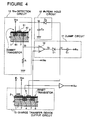
- FIG 4 there is shown a circuit diagram of a first embodiment of the charge transfer device in accordance with the present invention.
- elements corresponding to those shown in Figure 1 are given the same Reference Numerals, and explanation thereof will be omitted.
- the shown charge transfer device has a ⁇ RH detection circuit 10 for detecting a potential ⁇ RH of a channel under a reset gate 5 when the reset pulse ⁇ R is at a high level, and a clamp circuit 11 including a comparator 14, a diode D1 having an anode connected to an output of the comparator 14, and a capacitor C1 having one end connected to a cathode of the diode D1.
- the shown charge transfer device also includes a ⁇ R peak hold circuit 12 composed of a diode D2 having an anode connected to the cathode of the diode D1 and a capacitor C2 having one end connected to an anode of the diode D2 and the other connected to ground.
- the ⁇ R peak hold circuit 12 operates to hold a high level of the reset pulse ⁇ R .
- Reference Numeral 13 designates an output circuit of a charge transfer device to be properly operated.
- the ⁇ RH detection circuit 10 includes a MOS transistor composed of a source region 41 and a drain region 61 formed in the p-type substrate 1, and an n-type diffusion region 7 formed between the source region 41 and the drain region 61.
- the insulating layer 2 covers the source region 41, the n-type diffusion region 7 and the drain region 61 formed in the p-type substrate 1.
- a gate electrode 51 is formed on the insulating layer 2 above the n-type diffusion region 7 formed between the source region 41 and the drain region 61.
- the MOS transistor of the ⁇ RH detection circuit 10 is a dummy transistor having the same characteristics in size, in voltage gain, in threshold and in others, as those of a MOS transistor (the reset transistor) formed of the floating diffusion 4, the reset gate 5 and the reset drain 6 in the charge transfer device output circuit 13.
- the drain 61 of the dummy transistor is connected to a high voltage V DD which is not less than the reset voltage V RD .
- the source 41 is grounded through a resistor R having a resistance which is several times of an on-resistance of the dummy transistor.
- the gate electrode 51 is connected to the cathode of the diode D2 of the ⁇ R peak hold circuit 12.
- an output voltage V4 of the comparator 14 rises.
- the rise of the output voltage V4 of the comparator 14 causes to raise a DC component of an output of V1 of the clamp circuit 11 which is a level shifted output of an input pulse ⁇ R1 .
- the output of V1 of the clamp circuit 11 is applied to the reset gate 5 as the reset pulse, and a peak value of the output V1 of the clamp circuit 11 is held in the ⁇ R peak hold circuit 12.
- the output voltage V2 of the ⁇ R peak hold circuit 12 is lower than the peak value of the clamp circuit output V1 by the forward direction voltage drop V F of the diode D2.
- the high level of the reset pulse ⁇ R is higher than a required minimum voltage by the forward direction voltage drop V F of the diode D2. Since this forward direction voltage V F of the diode D2 exists as a voltage margin, it is preferable. Thus, an ideal high level of the reset pulse ⁇ R can be set.
- the first embodiment shown in Figure 4 operates to automatically adjust the reset pulse ⁇ R to the effect that the potential ⁇ RH of the channel under the reset gate 5 is ceaselessly consistent with the reset voltage V RD (or slightly deeper than V RD ). Therefore, it is possible to avoid the disadvantage in which the channel potential ⁇ RH varies in relation to the same reset pulse ⁇ R . In addition, it is also possible to avoid a troublesome or complicated procedure of a resistance adjustment for the level adjustment of the reset pulse ⁇ R .
- FIG 7 there is shown a circuit diagram of a second embodiment of the charge transfer device in accordance with the present invention.
- elements corresponding to those shown in Figure 4 are given the same Reference Numerals, and a detail explanation thereof will be omitted.
- the second embodiment of the charge transfer device in accordance with the present invention includes the ⁇ RH detection circuit 10 for detecting the potential ⁇ RH of the channel under the reset gate 5 when the reset pulse ⁇ R is at the high level, the ⁇ R peak hold circuit 12 for holding the peak level of the reset pulse ⁇ R , and an output circuit 13 of the charge transfer device, similarly to the first embodiment.
- the second embodiment does not include the clamp circuit 12 provided in the first embodiment.
- the second embodiment is characterized in that the high level and the low level of the reset pulse ⁇ R are fixed, and the source 41 of the dummy transistor is directly connected to the reset drain 6 of the reset transistor and also grounded through a capacitor C3. Therefore, the second embodiment does not control the high level of the reset pulse ⁇ R .
- the second embodiment is configured to cause the drain voltage V RD to follow the potential ⁇ RH of the channel under the reset gate when the fixed high level of the reset pulse ⁇ R is applied.
- the ⁇ R peak hold circuit 12 holds a high level of the reset pulse ⁇ R , and outputs an output voltage V12, which is consistent with the high level of the reset pulse ⁇ R , if it is assumed that the forward direction voltage drop of the diode D2 is zero.
- the output voltage V12 is applied to the gate 51 of the dummy transistor.
- the channel potential of the dummy transistor becomes equal to the channel potential ⁇ RH of the reset transistor when the reset pulse ⁇ R is at the high level, similarly to the first embodiment. Therefore, this channel potential ⁇ RH is outputted from the dummy transistor in the form of the source voltage V11 of the dummy transistor and applied to the reset drain 6 of the reset transistor.
- the channel potential ⁇ RH at the time of resetting can be made consistent with the potential of the reset drain. Accordingly, it is possible to avoid a troublesome level adjustment of the reset pulse ⁇ R .
- the second embodiment has a circuit construction greatly simpler than that of the first embodiment.
- the above mentioned embodiments have been a buried channel type charge transfer device.
- the present invention can be applied to a surface channel type charge transfer device.
- the conduction type of the respective regions in the charge transfer devices can also be inverted, the present invention can also be applied.
- a buffer can be inserted between the source 41 of the dummy transistor and the reset drain of the reset transistor. In this modification, it is possible to suppress a potential variation occurring at the time of the resetting.
- the charge transfer circuit in accordance with the present invention is characterized in that the potential of the channel under the reset gate is detected so that a minimum reset pulse voltage or reset drain voltage required for completing the resetting of the reset transistor is automatically applied to the reset gate or the reset drain.
- the variation of the channel potential under the reset gate caused by the manufacture variation can be compensated, and therefore, the troublesome voltage adjustment procedure for the reset pulse can be omitted.
- the channel potential and the reset drain voltage can be made substantially equal, a voltage operation margin of the device itself can be consequentially enlarged.
Landscapes
- Solid State Image Pick-Up Elements (AREA)
Claims (8)
- Dispositif de transfert de charge comprenant :- une section de transfert de charge ayant une région de transfert de charge formée dans un substrat semi-conducteur (1) et des électrodes de transfert (2a, 2b, 2c) formées sur ledit substrat semi-conducteur (1);- un transistor de remise à zéro (4, 5, 6) ayant une région de diffusion flottante (4) formée dans ledit substrat semi-conducteur (1) pour recevoir une charge électrique transférée de ladite section de transfert de charge, un drain de remise à zéro (6) où est appliquée une tension de remise à zéro (VRD), et une grille de remise à zéro (5) formée au-dessus d'un canal (7) entre ladite région de diffusion flottante (4) et ledit drain de remise à zéro (6), une impulsion de remise à zéro (φR; V₁) étant appliquée à ladite grille de remise à zéro (5); et- des moyens de détection de potentiel (10) pour détecter un potentiel d'un canal dudit transistor de remise à zéro (4, 5, 6) lorsque ledit transistor de remise à zéro est dans une opération de remise à zéro;caractérisé par :
- des moyens de suivi de tension (11) pour que ledit potentiel dudit canal (7) dudit transistor de remise à zéro suive ladite tension de remise à zéro (VRD) lorsque ledit transistor de remise à zéro est dans ladite opération de remise à zéro. - Dispositif de transfert de charge selon la revendication 1, comprenant en outre un circuit de maintien de crête (12) connecté à son entrée à ladite grille de remise à zéro (5) dudit transistor de remise à zéro pour maintenir un niveau de crête de ladite tension de remise à zéro et dans lequel lesdits moyens de détection de potentiel (10) comprennent un transistor fictif ayant un drain (61) connecté pour recevoir une tension (VDD) ayant une valeur absolue supérieure à celle de ladite tension de remise à zéro, une source (41) reliée à la masse par une résistance (R) ayant une résistance qui est considérablement supérieure à une résistance à l'état passant dudit transistor fictif lui-même, et une électrode de grille (51) connectée à une sortie dudit circuit de maintien de crête (12), ledit transistor fictif ayant les mêmes caractéristiques que celles dudit transistor de remise à zéro.
- Dispositif de transfert de charge selon la revendication 2, dans lequel ledit circuit de maintien de crête (12) comprend une diode (D₂) ayant une anode connectée à ladite grille de remise à zéro (5) dudit transistor de remise à zéro et une cathode connectée à ladite grille (51) dudit transistor fictif, et un condensateur (C₂) ayant une extrémité connectée à ladite cathode de ladite diode et l'autre extrémité connectée à la masse.
- Dispositif de transfert de charge selon la revendication 1, comprenant en outre un circuit de blocage (11) ayant un comparateur (14) ayant une première entrée connectée audit drain (41) dudit transistor fictif et une deuxième entrée connectée audit drain de remise à zéro (6) dudit transistor de remise à zéro, une deuxième diode (D₁) ayant une anode connectée à une sortie dudit comparateur (14) et une cathode connectée à ladite grille de remise à zéro (5) dudit transistor de remise à zéro.
- Dispositif de transfert de charge selon la revendication 1, dans lequel lesdits moyens de suivi de tension fonctionnent de manière à rendre consistant le potentiel du canal (7) dudit transistor de remise à zéro, lorsque ledit transistor de remise à zéro est dans l'opération de remise à zéro, avec ladite tension de remise à zéro (VRD).
- Dispositif de transfert de charge comprenant :- une section de transfert de charge ayant une région de transfert de charge formée dans un substrat semi-conducteur (1) et des électrodes de transfert (2a, 2b, 2c) formées sur ledit substrat semi-conducteur (1);- un transistor de remise à zéro ayant une région de diffusion flottante (4) formée dans ledit substrat semiconducteur (1) pour recevoir une charge électrique transférée de ladite section de transfert de charge, un drain de remise à zéro (6) où est appliquée une tension de remise à zéro (V₁₁), et une grille de remise à zéro (5) formée au-dessus d'un canal entre ladite région de diffusion flottante (4) et ledit drain de remise à zéro (6), une impulsion de remise à zéro (φR) étant appliquée à ladite grille de remise à zéro (5);- des moyens de détection de potentiel (10) pour détecter un potentiel d'un canal dudit transistor de remise à zéro lorsque ledit transistor de remise à zéro est dans une opération de remise à zéro;- des moyens de suivi de tension pour que ladite tension de remise à zéro (V₁₁) suive la tension détectée par lesdits moyens de détection de potentiel (10) lorsque ledit transistor de remise à zéro est dans ladite opération de remise à zéro;caractérisé en ce qu'il comprend en outre :
- un circuit de maintien de crête (12) connecté à ladite grille de remise à zéro (5) dudit transistor de remise à zéro pour maintenir un niveau de crête de ladite tension de remise à zéro et dans lequel lesdits moyens de détection de potentiel (10) comprennent un transistor fictif ayant un drain (61) connecté pour recevoir une tension ayant une valeur absolue supérieure à celle de ladite tension de remise à zéro, une source (41) reliée à la masse par une résistance (R) ayant une résistance qui est considérablement supérieure à une résistance à l'état passant dudit transistor fictif lui-même, et une électrode de grille (51) connectée à une sortie dudit circuit de maintien de crête (12), ledit transistor fictif ayant les mêmes caractéristiques que celles dudit transistor de remise à zéro, ledit drain (41) dudit transistor fictif étant directement connecté audit drain de remise à zéro (6) dudit transistor de remise à zéro. - Dispositif de transfert de charge selon la revendication 6, dans lequel ledit circuit de maintien de crête (12) comprend une diode (D₂) ayant une anode connectée à ladite grille de remise à zéro (5) dudit transistor de remise à zéro et une cathode connectée à ladite grille (51) dudit transistor fictif, et un condensateur (C₂) ayant une extrémité connectée à ladite cathode de ladite diode et l'autre extrémité connectée à la masse.
- Dispositif de transfert de charge selon la revendication 6, dans lequel lesdits moyens de suivi de tension fonctionnent de manière à rendre consistante ladite tension de remise à zéro, lorsque ledit transistor de remise à zéro est dans l'opération de remise à zéro, avec la tension détectée par lesdits moyens de détection de potentiel.
Applications Claiming Priority (2)
| Application Number | Priority Date | Filing Date | Title |
|---|---|---|---|
| JP58989/90 | 1990-03-10 | ||
| JP2058989A JP2707784B2 (ja) | 1990-03-10 | 1990-03-10 | 電荷転送装置 |
Publications (3)
| Publication Number | Publication Date |
|---|---|
| EP0447917A2 EP0447917A2 (fr) | 1991-09-25 |
| EP0447917A3 EP0447917A3 (en) | 1992-01-08 |
| EP0447917B1 true EP0447917B1 (fr) | 1995-12-20 |
Family
ID=13100258
Family Applications (1)
| Application Number | Title | Priority Date | Filing Date |
|---|---|---|---|
| EP91103715A Expired - Lifetime EP0447917B1 (fr) | 1990-03-10 | 1991-03-11 | Dispositif de transfert de charge |
Country Status (4)
| Country | Link |
|---|---|
| US (1) | US5224134A (fr) |
| EP (1) | EP0447917B1 (fr) |
| JP (1) | JP2707784B2 (fr) |
| DE (1) | DE69115527T2 (fr) |
Families Citing this family (3)
| Publication number | Priority date | Publication date | Assignee | Title |
|---|---|---|---|---|
| JPH07105489B2 (ja) * | 1993-05-27 | 1995-11-13 | 日本電気株式会社 | 電荷転送装置 |
| JP3031815B2 (ja) * | 1994-04-01 | 2000-04-10 | シャープ株式会社 | 電荷検出素子及びその製造方法並びに電荷転送検出装置 |
| US6858917B1 (en) * | 2003-12-05 | 2005-02-22 | National Semiconductor Corporation | Metal oxide semiconductor (MOS) bandgap voltage reference circuit |
Family Cites Families (5)
| Publication number | Priority date | Publication date | Assignee | Title |
|---|---|---|---|---|
| JPS61131854U (fr) * | 1985-02-06 | 1986-08-18 | ||
| NL8500863A (nl) * | 1985-03-25 | 1986-10-16 | Philips Nv | Ladingsoverdrachtinrichting. |
| DE3852320T2 (de) * | 1987-05-21 | 1995-04-06 | Toshiba Kawasaki Kk | Ladungsübertragungsanordnung. |
| JP2672507B2 (ja) * | 1987-05-21 | 1997-11-05 | 株式会社東芝 | 電荷転送素子 |
| JPH084137B2 (ja) * | 1988-01-12 | 1996-01-17 | 日本電気株式会社 | 電荷転送装置の出力回路 |
-
1990
- 1990-03-10 JP JP2058989A patent/JP2707784B2/ja not_active Expired - Lifetime
-
1991
- 1991-03-11 US US07/667,155 patent/US5224134A/en not_active Expired - Fee Related
- 1991-03-11 DE DE69115527T patent/DE69115527T2/de not_active Expired - Fee Related
- 1991-03-11 EP EP91103715A patent/EP0447917B1/fr not_active Expired - Lifetime
Also Published As
| Publication number | Publication date |
|---|---|
| JP2707784B2 (ja) | 1998-02-04 |
| DE69115527T2 (de) | 1996-07-18 |
| EP0447917A3 (en) | 1992-01-08 |
| DE69115527D1 (de) | 1996-02-01 |
| EP0447917A2 (fr) | 1991-09-25 |
| US5224134A (en) | 1993-06-29 |
| JPH03261150A (ja) | 1991-11-21 |
Similar Documents
| Publication | Publication Date | Title |
|---|---|---|
| US7110030B1 (en) | Solid state image pickup apparatus | |
| US5191398A (en) | Charge transfer device producing a noise-free output | |
| JP3310164B2 (ja) | 固体撮像装置 | |
| US6600513B1 (en) | Charge transfer device | |
| KR100272648B1 (ko) | 전하전송장치 | |
| EP0447917B1 (fr) | Dispositif de transfert de charge | |
| EP0280097B1 (fr) | Dispositif de transfert de charge avec circuit amplificateur | |
| EP0377959B1 (fr) | Méthode pour commander un circuit de détection de charge | |
| JPS6233751B2 (fr) | ||
| US5208474A (en) | Input circuit of a semiconductor device | |
| US7088393B1 (en) | Output-compensated buffers with source-follower input structure, methods of operating same, and image capture devices using same | |
| JPS61224357A (ja) | 電荷転送装置 | |
| US4631739A (en) | High dynamic range charge amplifier | |
| JPS6251508B2 (fr) | ||
| US4700085A (en) | Circuit for detecting signal charges transferred in a charge transfer device | |
| EP0311529B1 (fr) | Capteur d'images comportant des régions de stockage de charges | |
| US5172399A (en) | Semiconductor charge transfer device including charge quantity detection | |
| US6797935B2 (en) | Method of charging the photodiode element in active pixel arrays | |
| US6201268B1 (en) | Output structure of charge-coupled device and method for fabricating the same | |
| US5336910A (en) | Charge coupled device of high sensitivity and high integration | |
| KR910006247B1 (ko) | 전하전송소자 | |
| US5612554A (en) | Charge detection device and driver thereof | |
| US6191440B1 (en) | Charge transfer device with improved charge detection sensitivity | |
| US7109784B2 (en) | Gate bias circuit for MOS Charge Coupled Devices | |
| JPH089257A (ja) | 昇圧回路及びこれを用いた固体撮像装置 |
Legal Events
| Date | Code | Title | Description |
|---|---|---|---|
| PUAI | Public reference made under article 153(3) epc to a published international application that has entered the european phase |
Free format text: ORIGINAL CODE: 0009012 |
|
| 17P | Request for examination filed |
Effective date: 19910311 |
|
| AK | Designated contracting states |
Kind code of ref document: A2 Designated state(s): DE FR GB NL |
|
| PUAL | Search report despatched |
Free format text: ORIGINAL CODE: 0009013 |
|
| AK | Designated contracting states |
Kind code of ref document: A3 Designated state(s): DE FR GB NL |
|
| 17Q | First examination report despatched |
Effective date: 19940914 |
|
| GRAA | (expected) grant |
Free format text: ORIGINAL CODE: 0009210 |
|
| AK | Designated contracting states |
Kind code of ref document: B1 Designated state(s): DE FR GB NL |
|
| REF | Corresponds to: |
Ref document number: 69115527 Country of ref document: DE Date of ref document: 19960201 |
|
| ET | Fr: translation filed | ||
| PLBE | No opposition filed within time limit |
Free format text: ORIGINAL CODE: 0009261 |
|
| STAA | Information on the status of an ep patent application or granted ep patent |
Free format text: STATUS: NO OPPOSITION FILED WITHIN TIME LIMIT |
|
| 26N | No opposition filed | ||
| PGFP | Annual fee paid to national office [announced via postgrant information from national office to epo] |
Ref country code: DE Payment date: 20010306 Year of fee payment: 11 |
|
| PGFP | Annual fee paid to national office [announced via postgrant information from national office to epo] |
Ref country code: GB Payment date: 20010307 Year of fee payment: 11 |
|
| PGFP | Annual fee paid to national office [announced via postgrant information from national office to epo] |
Ref country code: FR Payment date: 20010313 Year of fee payment: 11 |
|
| PGFP | Annual fee paid to national office [announced via postgrant information from national office to epo] |
Ref country code: NL Payment date: 20010330 Year of fee payment: 11 |
|
| REG | Reference to a national code |
Ref country code: GB Ref legal event code: IF02 |
|
| PG25 | Lapsed in a contracting state [announced via postgrant information from national office to epo] |
Ref country code: GB Free format text: LAPSE BECAUSE OF NON-PAYMENT OF DUE FEES Effective date: 20020311 |
|
| PG25 | Lapsed in a contracting state [announced via postgrant information from national office to epo] |
Ref country code: NL Free format text: LAPSE BECAUSE OF NON-PAYMENT OF DUE FEES Effective date: 20021001 Ref country code: DE Free format text: LAPSE BECAUSE OF NON-PAYMENT OF DUE FEES Effective date: 20021001 |
|
| GBPC | Gb: european patent ceased through non-payment of renewal fee |
Effective date: 20020311 |
|
| PG25 | Lapsed in a contracting state [announced via postgrant information from national office to epo] |
Ref country code: FR Free format text: LAPSE BECAUSE OF NON-PAYMENT OF DUE FEES Effective date: 20021129 |
|
| NLV4 | Nl: lapsed or anulled due to non-payment of the annual fee |
Effective date: 20021001 |
|
| REG | Reference to a national code |
Ref country code: FR Ref legal event code: ST |