EP0448142A2 - Filterschaltung mit geschalteten Kapazitäten - Google Patents
Filterschaltung mit geschalteten Kapazitäten Download PDFInfo
- Publication number
- EP0448142A2 EP0448142A2 EP91200464A EP91200464A EP0448142A2 EP 0448142 A2 EP0448142 A2 EP 0448142A2 EP 91200464 A EP91200464 A EP 91200464A EP 91200464 A EP91200464 A EP 91200464A EP 0448142 A2 EP0448142 A2 EP 0448142A2
- Authority
- EP
- European Patent Office
- Prior art keywords
- switched capacitor
- terminal
- input
- output
- circuit
- Prior art date
- Legal status (The legal status is an assumption and is not a legal conclusion. Google has not performed a legal analysis and makes no representation as to the accuracy of the status listed.)
- Withdrawn
Links
Images



Classifications
-
- H—ELECTRICITY
- H03—ELECTRONIC CIRCUITRY
- H03H—IMPEDANCE NETWORKS, e.g. RESONANT CIRCUITS; RESONATORS
- H03H19/00—Networks using time-varying elements, e.g. N-path filters
- H03H19/004—Switched capacitor networks
Definitions
- This invention relates to a switched capacitor filter circuit.
- Switched capacitor circuits and operational amplifiers are widely used in both fixed and adjustable filters.
- Such switched capacitor type filters generally rely upon the effective resistance of a switched capacitor circuit to set filter coefficients.
- the effective resistance of a switched capacitor circuit is determined by the value of the capacitor and the frequency of the clock signals controlling the associated switches.
- the frequency of the circuit clock signals is generally constrained to be substantially higher than the frequency of the signals processed by the filter.
- the higher frequency clock rate must be a integral multiple of the lower clock rate. Accordingly, varying the filter clocking frequency is generally not a practical way of adjusting filter parameters.
- the invention seeks to provide an improved switched capacitor filter circuit.
- an aspect of the present invention provides a switched capacitor filter circuit as defined in claim 1.
- the circuit comprises a switched capacitor coupler having an effective resistance determined by the magnitude of an input signal applied thereto.
- the magnitude of the input signal applied to the switched capacitor coupler can be varied to adjust the effective resistance thereof.
- the magnitude of the input signal is preferably infinitely adjustable.
- the input signal is coupled to a filter by the switched capacitor coupler, sush that the magnitude of the input signal is varied to determine the exhibited effective resistance of the switched capacitor coupler and thereby to vary the parameters of the filter.
- the switched capacitor filter circuit comprises a summing circuit, an integrator and a switched capacitor arrangement coupling the summing circuit and the integrator.
- An input signal is applied to the summing circuit and the output therefrom is supplied to the integrator through the switched capacitor coupler.
- the switched capacitor coupler operates as an effective resistance for the integrator to control one or more parameters of the filter circuit.
- a voltage controlled attenuator interposed between the output of the summing circuit and the switched capacitor coupler determines the effective resistance.
- the voltage controlled attenuator provides a controlled reduced replica of the summing circuit output which sets the charging voltage for the switched capacitor coupler in accordance with a control source.
- the effective resistance of the switched capacitor coupler and the filter parameters can thereby be made infinitely adjustable.
- the filter 100 comprises an input terminal 110, an input and summing circuit 101, a switched capacitor coupling network 104, an integrator circuit 102, a switched capacitor feedback circuit 106, an output terminal 112, voltage source terminals 114 and 118, and a switched capacitor clock signal source 120 which generates output clock signals 1, 1' (the complement of 1), 2 and 2' (the complement of 2).
- Input and summing circuit 101 may comprise an operational amplifier in combination with switched capacitor elements of any suitable type.
- Supply voltages +VDD/2 and +VDD when applied to terminals 114 and 118, respectively, supply power to the input and summing circuit 101.
- Integrator circuit 102 may include an operational amplifier (not shown) and associated coupling elements (not shown).
- Switched capacitor coupling network 104 and switched capacitor feedback circuit 106 may each comprise arrangements of switched capacitor and capacitor elements adapted to determine the forward coupling and feedback transfer functions of the filter 100.
- An input signal VIN applied to terminal 110 of Figure 1 is fed to an input of the input and summing circuit 101 and is combined therein with signals fed back from integrator circuit 102 via switched capacitor feedback circuit 106.
- Terminal 110 is also coupled to another input of switched capacitor coupling network 104.
- Switched capacitor coupling network 104 couples the output of the input and summing circuit 101 to integrator circuit 102.
- the arrangement of switched capacitor elements within coupling network 104 and integrator circuit 102 and in switched capacitor feedback circuit 106 determine the transfer characteristic of the filter circuit 100.
- the general form of filter 100 is useful in constructing low-pass filters, band-pass filters, notch filters, etc. by various configuration of the switched capacitors and other elements.
- the transfer characteristics of the switched capacitor filter 100 may be made fixed or adjustable.
- a switched capacitor may simulate a resistance by transferring packets of charge from one circuit terminal, e.g. 801, to another, e.g. 830.
- the switched capacitor arrangement in Figure 8 comprises capacitor 805 and substantially identical bi-directional transmission gates 832, 835, 840 and 845.
- Transmission gate 832 comprises an n-channel field effect transistor 803 and a p-channel field effect transistor 807 which passes current under control of a clock signal.
- the drain of transistor 803 is connected to the source of transistor 807 and the source of transistor 803 is connected to the drain of transistor 807.
- a clock signal 1 is applied to the gate of transistor 803 and at the same time the complement of clock signal 1, 1', is applied to the gate of transistor 807. Both transistors 803 and 807 are switched to their on states in response to the clock signals applied to their respective gates so that a bi-directional current path is formed.
- Bi-directional transmission gate 835 comprises n-channel field effect transistor 810 and p-channel field effect transistor 812.
- the bi-directional transmission gates 832 and 835 are closed (low impedance paths) at the same time in response to the 1 clock signals applied thereto, thereby completing the current path from terminal 801 to terminal 830.
- Bi-directional gate 840 comprises n-channel field effect transistor 815 and p-channel field effect transistor 817 and is connected between terminal 822 and one side of capacitor 805.
- bi-directional transmission gate 845 comprises n-channel field effect transistor 820 and p-channel field effect transistor 824 and is connected between terminal 825 and the other side of capacitor 805. Both bi-directional transmission gates 840 and 845 are controlled by clock signal 2 and its complement, 2'.
- Clock signals 1 and 2 are of opposite phase and are non-overlapping.
- clock signal 1 causes bi-directional transmission gates 832 and 835 to conduct
- clock signal 2 prevents conduction of bi-directional transmission gates 840 and 845.
- clock signal 2 activates bi-directional transmission gates 840 and 845
- bi-directional transmission gates 832 and 835 are rendered non-conductive by clock signal 1.
- each bi-directional transmission gate described with respect to Figure 8 is shown as a rectangle labelled T with input and output terminals and a designated clock signal and its complement applied thereto.
- capacitor 805 receives a charge packet corresponding to the voltage across terminals 822 and 825 while bi-directional transmission gates 840 and 845 conduct in response to clock signal 2. bi-directional transmission gates 832 and 835 are non-conducting at this time.
- the capacitor 805 In the time period when clock signal 2 is off and clock signal 1 is on, the capacitor 805 is discharged through bi-directional transmission gates 832 and 835, while the charging path through bi-directional transmission gates 840 and 845 is disabled, being effectively an open circuit.
- the process is repeated at a high rate relative to the frequency of the signal applied to terminal 801.
- the charge packets appear as a steady current.
- the current flow through bi-directional transmission gates 832 and 835 i.e. the charge transferred per unit time, is a function of the clock rate of signals 1 and 2, the size of capacitor 805, and the voltage applied between terminals 822 and 825. Consequently, the equivalent resistance of the switched capacitor arrangement in Figure 8 is proportional to 1/fC where f is the clock frequency and C is the capacitance of capacitor 805.
- External resistors may be used to vary the filter parameters of the fixed switched capacitor filter circuit 100 of Figure 1 so that modifications to the switched capacitor arrangement are not required for such variations.
- the use of external resistors precludes full integration of the filter into an integrated circuit and requires highly accurate resistor values.
- Changes of filter characteristics in a circuit such as the switched capacitor filter 100 in Figure 1 may also be accomplished by varying capacitance, e.g., the capacitance of capacitor 805 in the switched capacitor element of Figure 8. Additional capacitors can be placed in parallel across capacitor 805. This technique, however, only permits variation in discrete steps.
- the voltage across capacitor 805 may be changed by charging through an integrator with a fixed time constant through a programmed number of clock cycles. However, the number of clock cycles can only be varied in discrete steps. Neither of these methods nor adjustment of the clock rate of transmission gates illustrated in Figure 8 allow continuous, or infinite adjustment of filter characteristics.
- Such adjustment can be achieved by attenuating the signal applied to the switched capacitor coupling network and adjusting the attenuation so that the amount of charge in the capacitor of the switched capacitor coupler, e.g., coupling network 104 in Figure 1, can be infinitely adjusted on the basis of an external control signal.
- the filter 200 comprises an input terminal 210, an input and summing circuit 201, a variable attenuator 208, a switched capacitor coupling network 204, an integrator circuit 202, a switched capacitor feedback circuit 206, an output terminal 212, voltage source terminals 214 and 218 and a switched capacitor clock signal source 220 which generates clock signals 1, 1', 2 and 2' which are coupled to inputs of the input and summing circuit 201, the network 204, the integrator circuit 202 and the network 206.
- Variable attenuator 208 receives a control signal VC from an input control terminal 216.
- Voltage VC is infinitely adjustable and determines the attenuation parameters of variable attenuator 208.
- the input and summing circuit 201, the integrator circuit 202 and the switched capacitor coupling and feedback circuits 204 and 206 include switched capacitor elements and receive switched capacitor clock signals 1 and 2 from clock signal source 220.
- Input and summing circuit 201 may comprise an operational amplifier in combination with switched capacitor elements of any suitable type.
- Integrator circuit 202 may include an operational amplifier and associated coupling elements.
- Variable attenuator 208 may be any attenuator well known in the art having its attenuation controlled by an external control signal. In the preferred embodiment, the arrangements disclosed in co-pending European patent application No. (RJ/3457) filed the same day as this application, are used in the summing circuit 201 and the variable attenuator 208.
- Switched capacitor coupling network 204 and switched capacitor feedback circuit 206 may each comprise arrangements of switched capacitor and capacitor elements adapted to determine the forward coupling and feedback transfer functions of the filter 200.
- the operation of the filter 200 is similar to that described with respect to the filter 100 of Figure 1 except for the variable attenuator 208, interposed between the input and summing circuit 201 and the switched capacitor coupling network 204.
- the input signal VIN from terminal 210 is fed to the input and summing circuit 201 and is combined therein with signals fed back from the integrator circuit 202 via the switched capacitor feedback circuit 206.
- the output of input and summing circuit 201 is supplied to switched capacitor coupling network 204 through variable attenuator 208.
- the magnitude of the output signal from the variable attenuator 208 is determined by a control voltage VC, which is infinitely adjustable. In this way, the filter 200 coefficients affected by the switched capacitor coupling network 204 may be infinitely adjusted, rather than being adjustable only in discrete steps.
- Switched capacitor coupling circuit 204 receives an output signal from the variable attenuator 208. As explained with respect to the switched capacitor element shown in Figure 8, the voltage charging the capacitor in such a switched capacitor element determines its effective resistance. In this way, the effective resistance in switched capacitor coupling network 204 can be infinitely adjusted, by adjusting the input voltage.
- An output of switched capacitor coupling network 204 is coupled to an input of integrator circuit 202 which further determines the transfer function of the filter 200.
- a signal VOUT at the output of integrator 202 (a terminal 212) is fed back to the input and summing circuit 201 through switched capacitor feedback circuit 206 to determine further the transfer characteristic of filter 200 and to stabilize its operation.
- the general form of the switched capacitor filter 200 is useful in constructing low-pass filters, band-pass filters, notch filters, etc. by various configurations of the switched capacitors and other elements. Additionally, the filter coefficients and the resultant transfer function can be infinitely adjusted by adjustment of control voltage VC and by means of the variable attenuator 208.
- the filter 300 comprises an input terminal 310, a summing circuit 301 (shown within dashed lines) corresponding to input and summing circuit 201 of Figure 2, a variable attenuator 308 corresponding to attenuator 208 of Figure 2, a switched capacitor coupling network 304 (shown within dashed lines) corresponding to coupling network 204 of Figure 2, an integrator 302 (shown within dashed lines) corresponding to integrator 202 of Figure 2, and a switched capacitor feedback circuit 306 (shown within dashed lines) comprising transmission gates 352 and 354 and capacitors 356 and 360.
- the summing circuit 301 comprises transmission gates 305, 307, 309 and 311, a capacitor 313, an operational amplifier 320 and a feedback capacitor 328.
- the switched capacitor coupling network 304 comprises transmission gates 333, 335, 340 and 342 and a capacitor 338.
- the integrator 302 comprises an operational amplifier 344 and a feedback capacitor 330.
- input signal VIN from terminal 310 is fed to a negative (-) input terminal 325 of operational amplifier 320 through the switched capacitor arrangement of 1 (and 1') clocked transmission gates 309,311, 2 (and 2') clocked transmission gates 305,307 and capacitor 313.
- Transmission gates 305 and 309 and a terminal 314 are connected to a voltage source having an output voltage of VDD/2.
- a positive input (+) of operational amplifier 320 is connected to a terminal 314.
- the output of integrator 302 is also fed to negative input 325 of operational amplifier 320 through 1 clocked transmission gates 352 and 311, and is affected by the 2 clocked transmission gates 354 and 305.
- Signal VIN from capacitor 313 is combined with the signal fed back from operational amplifier 344 at terminal 362, and is then fed to the negative input terminal 325 of operational amplifier 320.
- the output of operational amplifier 320 is supplied to switched capacitor coupling network 304 through variable attenuator 308.
- Switched capacitor coupling circuit 304 receives the output of variable attenuator 308. As explained with respect to the switched capacitor element shown in Figure 8, such a switched capacitor element functions as an effective resistance and the voltage charging the capacitor 338 determines this effective resistance. In this way, the effective resistance in switched capacitor coupling network 304 can be adjusted by adjusting the control voltage VC.
- capacitor 338 is charged through 2 clocked transmission gates 333 and 340 and discharged into the negative input of amplifier 344 at terminal 346 through 1 clocked transmission gates 335 and 342.
- the voltage at terminal 380 between attenuator 308 and transmission gate 333 is a replica of the signal from operational amplifier 320 at terminal 323. The magnitude of this replica signal is a function of voltage VC at terminal 316.
- the effective resistance of switched capacitor coupling network 304 is related to the centre operating frequency and the quality factor Q of the filter.
- the filter circuit 300 is an infinitely adjustable low-pass filter.
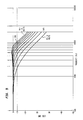
- the low-pass characteristics of the switched capacitor low-pass filter 300 for eight (8) different control voltagec at VC terminal 314 of Figure 3 are illustrated in Figure 5.
- a maximum control voltage e.g., 4 volts at terminal 316 in switched capacitor low-pass filter 300
- maximum bandwidth curve waveform 501
- a minimum control voltage e.g. 0.5 volts or less at terminal 316
- the output of the low-pass filter 300 is down approximately 3 dB at 10,000 Hz in the maximum bandwidth condition (waveform 501) and the output is down approximately 3 dB at 1,800 Hz in the minimum bandwidth condition (waveform 505).
- the output of the switched capacitor coupling network 304 is fed to the input of integrator circuit 302 which further determines the transfer function of filter 300.
- a signal VOUT from the output of integrator 302 at terminal 312 is fed back to input and summing circuit 301 to determine further the transfer characteristic of switched capacitor low-pass filter 300 and to stabilize its operation.
- Negative feedback from the output of operational amplifier 344 to the inverting (negative) input thereof at a terminal 346 is provided by the switched capacitor arrangement of transmission gates 352, 354, 340 and 342 and capacitor 356, and feedback capacitor 330.
- Negative feedback from the output of amplifier 344 to the inverting input 325 of amplifier 320 is provided by the transmission gates 352, 354, 305 and 311 and capacitor 360.
- variable attenuator such as the type employed as attenuator 308 may be used in place of the operational amplifier 344, whereby the effective resistance of the switched capacitor feedback network 306 may be varied to adjust the parameters of the feedback network in accordance with a control voltage similar to voltage VC.
- the switched capacitor circuit 300 may be used in audio type systems where voltage VIN applied to terminal 310 is an audio signal.
- Switched capacitor clock signals 1 and 2 may, for example, be non-overlapping square wave signals which occur at a 45 kHz repetition rate and the transmission gates shown in Figure 3 may be bi-directional transmission gates such as those illustrated in Figure 8.
- the voltage VDD/2 could be, for example, +4 volts.
- the output signal at terminal 312 is then the audio signal VIN modified by the transfer function of filter 300 in Figure 3 and centered about VDD/2.
- operational amplifier 320 that is the summing circuit 301, and attenuator 308 together comprise a dual output amplifier, as shown in Figure 6, described in our co-pending European patent application No. (RJ/3457) filed the same day as this application.
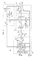
- Amplifier 600 comprises a differential input circuit 6103, a first output circuit 6104, a second output circuit 6106, a fixed bias source 6108, a variable bias source 6110, first and second load impedances 6112 and 6114 and a feedback element 6150.
- a first input terminal 6101 of amplifier 600 is coupled to a first input of differential input circuit 6103 and is shown coupled to an input signal POS.
- a second input terminal 6102 of amplifier 600 is coupled to a second input of differential input circuit 6103 and is shown coupled to an input signal NEG.
- Amplifier 600 generates a first output signal VOUT1 at a first output terminal 6116 of amplifier 600 which is coupled to an output of the first output circuit 6104, to a first terminal of load impedance 6112, and to a first terminal of feedback element 6150.
- Amplifier 600 generates a second output signal VOUT2 at a second output terminal 6118 of amplifier 600 which is coupled to an output of second output circuit 6106 and to a first terminal of load impedance 6114.
- First power supply terminals of the differential input circuit and the first and second output circuits 6104 and 6106 are coupled to a power supply Vdd and to a terminal 6160.
- Second terminals of load impedances 6112 and 6114 are coupled to a first power supply terminal of fixed bias source 6108, to a power supply Vdd/2 and to a terminal 6145.
- An input of variable bias source 6110 is coupled to a variable power supply VC (shown as VC with an arrow passing through it) and to a terminal 6120.
- a first output terminal of differential input circuit 6103 is coupled to first inputs of first and second output circuits 6104 and 6106 through a terminal 6130.
- a second output terminal of differential input circuit 6103 is coupled to second inputs of first and second output circuits 6104 and 6106 through a terminal 6133.
- An output of fixed bias source 6108 is coupled to power supply inputs of first output circuit 6104 and differential input circuit 6103 through terminal 6122.
- An output of variable bias source 6110 is coupled to a power supply input of second output circuit 6106 through a terminal 6123.
- a second terminal of feed back element 6150 is coupled to terminal 6101.
- Differential input circuit 6103 receives input signals POS and NEG from terminals 6101 and 6102, respectively, and forms an amplified signal corresponding to the difference between signals POS and NEG.
- the amplified differential signal appears across output terminals 6130 and 6133.
- the amplified signal from terminals 6130 and 6133 is fed to first output circuit 6104 and to second output circuit 6106.
- Signal VOUT1 is generated in the first output circuit 6104 and appears across load impedance 6112 between lead 6116 and terminal 6145.
- Terminal 6145 is effective as an A.C. ground.
- a separate output signal VOUT2 is obtained from the second output circuit 6106 and appears across load impedance 6114 between terminal 6118 and terminal 6145.
- Each of output circuits 6104 and 6106 operates independently in response to the bias voltages applied thereto from bias sources 6108 and 6110, respectively.
- Signals VOUT1 and VOUT2 are amplified versions of the signal corresponding to the difference between signals POS and NEG.
- the magnitude of signal VOUT1 from output circuit 6104, which is controlled by fixed bias source 6108, is independent of the magnitude of signal VOUT2 from output circuit 6106, which is controlled by variable bias source 6110.
- the output of fixed bias source 6108 supplies a bias control voltage to differential input circuit 6103 and to first output circuit 6104.
- the gain of output circuit 6104 is maintained at a prescribed level determined by fixed bias source 6108.
- Variable (adjustable) bias source 6110 which controls the gain of second output circuit 6106, receives a control voltage from the power supply VC.
- Control voltage VC may be infinitely adjusted so that the gain of second output circuit 6106 is adjustable. It is to be understood that additional output circuits substantially identical to second output circuit 6106 may be added to provide a plurality of output signals each controllable from a separate adjustable power supply.
- the gain of an operational amplifier is generally stabilized by providing a feedback path between its output and its input. Such a feedback path, however, interferes with any attempted adjustment of the gain by a bias source.
- a bias controlled variable signal from an operational amplifier is required, as in a switched capacitor arrangement.
- a bias controlled variable signal voltage is produced by an operational amplifier. The gain stability of the operational amplifier is assured by providing a feedback path between a fixed biased output stage and the input stage, while the gain of a variable biased output stage provides the needed bias controlled variable voltage.
- feedback element 6150 is shown coupled between terminal 6116 at the output of the fixed biased first output circuit 6104 and input terminal 6101 so that the operation of amplifier 600 is stabilized.
- Other known operational amplifier feedback arrangements may, of course, be used.
- Second output circuit is controlled by voltage VC through adjustable bias source 6110 whereby its gain is infinitely adjustable. In this way, a bias controlled variable voltage is produced by a gain stabilized operational amplifier.
- variable bias controlled output circuits similar to second output circuit 6106 may be added to amplifier 600 as long as one fixed bias controlled circuit such as output circuit 6104 is used.
- the addition of a feedback path between the output of the first output circuit 6104 and the differential input circuit further assures gain stability.
- FIG. 7 there is shown a schematic diagram of an amplifier circuit 700 that may be used as the operational amplifier 600 of Figure 6.
- Each of the block diagrams of Figure 6 is shown as a corresponding dashed line rectangle in Figure 7 with the same reference numbers used in Figures 6 and 7.
- Each of the circuits of Figure 7 comprises transistors and resistors coupled together to perform the desired function.
- Fixed bias source 6108 comprises resistors 7204 and 7209 and an n-p-n bipolar transistor 7205.
- Variable bias source 6110 comprises resistors 7281 and 7289 and an n-p-n bipolar transistor 7285.
- Differential input amplifier 6103 comprises p-channel field effect transistors 7220, 7222, 7225 and 7230, n-channel field effect transistors 7238 and 7240, n-p-n bipolar transistors 7207, 7232 and 7234, and a resistor 7290.
- First output circuit 6104 comprises p-channel field effect transistors 7244 and 7245, n-p-n bipolar transistors 7251, 7252 and 7255 and a resister 7260.
- Second output circuit 6106 comprises p-channel field effect transistors 7265 and 7269, n-p-n bipolar transistors 7272, 7275 and 7277, and a resistor 7280.
- all of the field effect transistors (FET) are typically metal-oxide-semiconductor transistors (MOSFETs).
- MOSFETs metal-oxide-semiconductor transistors
- the "metal" which is typically used for the gate, is polysilicon.
- Load impedances 6112 and 6114 are shown as resistors 6112 and 6114, respectively, and feedback element 6150 is shown as a resistor 6150a.
- a first terminal of resistor 7204 and first terminals of resistors 6112 and 6114 are coupled to a power supply having a positive output voltage of Vdd/2 and to the terminal 6145.
- the sources of transistors 7220, 7222, 7244, 7245, 7265 and 7269 are coupled to a power supply having a positive output voltage of Vdd and to the terminal 6160.
- First terminals of resistors 7209, 7260, 7280, 7289 and 7290, and the sources of transistors 7238 and 7240 are coupled to a reference power supply having a voltage of Vss (typically ground) and to the terminal 6161.
- Input terminal 6101 is coupled to the gate of transistor 7230 and to a first terminal of feedback resistor 6150a.
- Input terminal 6102 is coupled to the gate of transistor 7225.
- Output terminal 6116 is coupled to a second terminal of resistor 6112, to the collector of transistor 7252, to the drain of transistor 7245 and to a second terminal of feedback resistor 6150a.
- Output terminal 6118 is coupled to a second terminal of resistor 6114, to the collector of transistor 7272 and to the drain of transistor 7265.
- a second terminal of resistor 7204 is coupled to the collector and base of transistor 7205, to the bases of transistors 7207 and 7251 and to the terminal 6122.
- the emitter of transistor 7205 is coupled to a second terminal of the resistor 7209 and to a terminal 7304.
- a first terminal of resistor 7281 is coupled to a terminal 6120 and to a power supply having a variable output voltage VC which is shown as VC with an arrow passing through it.
- a second terminal of resistor 7281 is coupled to the base and collector of transistor 7285, to the base of transistor 7277 and to the terminal 6123.
- the emitter of transistor 7285 is coupled to a second terminal of the resistor 7289 and to a terminal 7306.
- the gates of transistors 7244 and 7245 are coupled to the drain of transistor 7244, to the collector of transistor 7255 and to a terminal 7308.
- the emitters of transistors 7252 and 7255 are coupled to the collector of transistor 7251 and to a terminal 7310.
- the emitter of transistor 7251 is coupled to a second terminal of resistor 7260 and to a terminal 7312.
- the bases of transistors 7232, 7255 and 7275 are coupled to the collector of transistor 7232, to the drain of transistor 7225 and to the terminal 6130.
- the bases of transistors 7234, 7252 and 7272 are coupled to the collector of transistor 7234, to the drain of transistor 7230 and to the terminal 6133.
- the gate of transistor 7265 is coupled to the gate and drain of transistor 7269, to the collector of transistor 7275 and to a terminal 7314.
- the emitters of transistors 7272 and 7275 are coupled to the collector of transistor 7277 and to a terminal 7316.
- the emitter of transistor 7277 is coupled to a second terminal of resistor 7280 and to a terminal 7318.
- the drain and gate of transistor 7220 are coupled to the collector of transistor 7207, to the gate of transistor 7222 and to a terminal 7320.
- the emitter of transistor 7207 is coupled to a second terminal of the resistor 7290 and to a terminal 7322.
- the drain of transistor 7222 is coupled to the sources of transistors 7225 and 7230 and to a terminal 7324.
- the emitter of transistor 7234 is coupled to the drain of transistor 7240 and to a terminal 7326.
- the emitter of transistor 7232 is coupled to the gate and drain of transistor 7238, to the gate of transistor 7240 and to a terminal 7328.
- the fixed bias source 6108 of the amplifier 700 of Figure 7 comprises a voltage divider arrangement connected between Vdd/2 (terminal 6145) and Vss (DC ground, terminal 6161).
- a preset voltage Vdd/2 applied to terminal 6145 causes a predetermined current to flow through the resistor 7204, the diode connected transistor 7205 and the resistor 7209.
- a preset voltage proportional to voltage Vdd/2 appears at the commonly connected base and collector (terminal 6122) of transistor 7205.
- This preset voltage is supplied to the bias arrangement (i.e., the base of transistor 7207) for source coupled transistors 7225 and 7230 of the differential input circuit 6103 of the amplifier 700 of Figure 7 and to the emitter bias arrangement for emitter coupled transistors 7252 and 7255 of the first output circuit 6104 of the amplifier 700 of Figure 7.
- the preset voltage Vdd/2 at terminal 6145 the gains of the differential input circuit 6103 and first output circuit 6104 portions of the amplifier in Figure 7 are fixed.
- the variable bias source 6110 of the amplifier of Figure 7 comprises a voltage divider arrangement connected between control voltage terminal 6120 and Vss (typically DC ground).
- An adjustable control voltage VC applied to terminal 6120 controls the current flow through the resistor 7281, the diode connected transistor 7285 and the resistor 7289.
- a voltage proportional to the adjustable control voltage VC appears at the commonly connected base and collector (terminal 6123) of transistor 7285.
- This adjustable voltage is supplied to the bias arrangement of the output circuit 6106 of the amplifier 700 of Figure 7 including emitter connected transistors 7272 and 7275.
- the gain of the second output circuit portion of the amplifier in Figure 7 may be infinitely adjusted by adjustment of the control voltage VC.
- input signals POS and NEG are applied to the gates of transistors 7225 and 7230, respectively.
- Transistors 7225 and 7230 operate as a source connected pair to amplify the difference between signals NEG and POS.
- the current for the sources of transistors 7225 and 7230 is coupled from the base of transistor 7205 of the fixed bias source 6108 to source connected transistors 7225 and 7230 through source bias transistor 7207 and current mirror connected transistors 7220 and 7222.
- the voltage at the base of transistor 7207 is controlled by the voltage at the collector and the base of transistor 7205.
- transistor 7207 Since the collector-base path of transistor 7207 is connected in series with the source-drain path of transistor 7220, the drain current through transistor 7220 and the drain current from transistor 7222 into terminal 7324 is fixed by the voltage VDD/2 at terminal 6145. Consequently, the current supplied to the source terminals of transistors 7225 and 7230 from terminal 7324 is predetermined.
- Diode connected transistors 7232 and 7234 and current mirror connected transistors 7238 and 7240 form an active load for the drains of transistors 7225 and 7230.
- the drain of transistor 7225 is connected to the drain and gate of transistor 7238 through the collector-emitter path of diode connected transistor 7232 while the drain of transistor 7230 is connected to the drain of transistor 7240 through the collector-emitter path of diode connected transistor 7234.
- the differential signal output of the input circuit 6103 of the amplifier 700 shown in Figure 7 appears between the drains of transistors 7225 and 7230.
- the gain of the amplifier input circuit 6103 in Figure 7 is determined by the source bias current which is in turn controlled by the base voltage of n-p-n source bias transistor 7207. Since this base voltage is fixed, the gain of the input circuit 6103 of Figure 7 is a preset and constant value.
- n-p-n transistor 7252 is connected to the drain of transistor 7230 and the base of transistor 7255 is connected to the drain of transistor 7225. These bases receive the differential output signal from input circuit transistors 7225 and 7230.
- the emitters of n-p-n transistors 7252 and 7255 are connected together at terminal 7310 and to a bias arrangement comprising the transistor 7257 and the resistor 7260 connected between terminal 7310 and Vss.
- the base of transistor 7251 is connected to the base of transistor 7205 in the fixed bias circuit 6108 of Figure 7. Consequently, the current through the collector-emitter path of transistor 7251 is controlled by the fixed voltage VDD/2 at terminal 6145.
- the gain of the first output circuit 6104 is thereby fixed with respect to the circuit bias as is the gain of input circuit 6103.
- n-p-n transistors 7252 and 7255 includes current mirror connected transistors 7244 and 7245 whose sources receive fixed DC voltage Vdd from terminal 6160 and load resistor 6112 connected between terminal 6145 and the collector of n-p-n transistor 7252.
- Transistor 7252 also has its collector connected to the drain of transistor 7245 as well as to resistor 6112.
- Transistor 7255 has its collector connected to the gates of transistors 7244 and 7245 and to the drain of transistor 7244 via terminal 7308.
- transistors 7252 and 7255 of the first output circuit 6104 in Figure 7 convert the differential voltage applied to their respective bases to an output current which flows through load resistor 6112 and produces a single ended output voltage VOUT1 at terminal 6116.
- the drain current through load transistor 7245 is the same as the collector current of n-p-n transistor 7252.
- a differential voltage appearing between the bases of n-p-n transistors 7252 and 7255 causes a net current flow through resistor 6112.
- a non-zero output voltage VOUT1 then appears at terminal 6116 relative to the AC ground at terminal 6145.
- Feedback element 6150 sets the gain and assures gain stability of the operational amplifier of Figure 7. In other applications, however, the feedback element is not used or stability may be assured by external feedback elements.
- the base of transistor 7272 is connected to the drain of transistor 7230 and the base of transistor 7275 is connected to the drain of transistor 7225.
- the emitters of n-p-n transistors 7272 and 7275 are connected together and to a bias arrangement provided at terminal 7316.
- the bias arrangement comprises series connected collector emitter path of n-p-n transistor 7277 and resistor 7280 connected between terminal 7314 and Vss (DC ground).
- the base of n-p-n transistor 7277 is connected to the base of transistor 7285 in the variable bias circuit 6110 of Figure 7. Consequently, the current through the collector-emitter path of n-p-n transistor 7277 is controlled by adjustable voltage VC at terminal 6120.
- the gain of the second output circuit is thereby rendered adjustable responsive to control voltage VC.
- the load circuit for transistors 7272 and 7275 includes current mirror connected transistors 7265 and 7269 whose drains receive fixed DC voltage Vdd and load resistor 6114 connected between voltage Vdd/2 carrying terminal 6145 and the collector of transistor 7272.
- Transistor 7272 has its collector connected to the drain of transistor 7265 as well as to resistor 6114 while the transistor 7275 has its collector connected to the drain and gate of transistor 7269 and to the gate of transistor 7265.
- Transistors 7272 and 7275 of the second output circuit portion in Figure 7 convert the differential voltage applied between their respective bases to an output current which flows through load resistor 6114 and provides an output signal VOUT2 at terminal 6118.
- the drain current of load transistor 7265 is equal to the collector current of transistor 7272. Consequently, no current flows through resistor 6114 and the voltage VOUT2 at terminal 6118 is equal to the voltage at terminal 6145, i.e., VDD/2.
- a differential voltage appearing between the bases of transistors 7272 and 7275 causes a net output current to flow through resistor 6114.
- a non-zero output voltage VOUT2 then appears at terminal 6118.
- the adjustable (variable) voltage VC in the circuit 700 of Figure 7 is received by the adjustable bias source 6110 and may be continuously adjustable in response to an external operating parameter.
- the adjustable voltage VC causes the voltage applied to the base of transistor 7277 in second output circuit 6106 to vary so that the gain of the second output circuit 6106 changes in accordance with the value of control voltage VC.
- the emitter bias current provided by transistor 7277 is varied from a minimum of zero to a maximum equal to the collector current in bias transistor 7251 of the amplifier first output circuit 6104 in Figure 7.
- the gain of the second output circuit 6106 in which emitter coupled transistors 7272 and 7275 are controlled by n-p-n bias transistor 7277 is adjustable between zero and the preset gain of the first output circuit 6104 controlled by bias transistor 7251.
- Vdd +8 volts
- Vdd/2 +4 volts
- Vss zero volts
- resistors 6112, 6114, 6150, 7204, 7209, 7260, 7280, 7281, 7289 and 7290 are 50K, 50K, 100K, 36K, 1.8K, 450, 450, 1.8K, 36K, and 1.8K ohms, respectively.
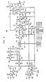
- the filter 400 comprises a pair of input terminals 401 and 405 for receiving an L-R signal and an L+R signal from an AM stereo receiver; a supply terminal 490 having a DC voltage VDD/2 applied thereto; a switched capacitor matrix circuit comprising transmission gates 407, 409, 411, 415, 425 and 428 and capacitors 420 and 422; a summing-type operational amplifier circuit comprising operational amplifier 435, transmission gates 468 and 488, a capacitor 440, and a feed-back capacitor 442; an externally controlled variable attenuator 408; a first switched capacitor coupling network comprising transmission gates 445, 448, 450, and 453 and a capacitor 480; a first integrator comprising an operational amplifier 455 and a feed-back capacitor 457; a second switched capacitor coupling network comprising transmission gates 458, 460, 462 and 467 and a capacitor 464; a second integrator comprising
- the filter 400 receives signals L-R and L+R at terminals 401 and 405, respectively, and operates to form a RIGHT channel signal minus a notch at 10 kHz (VNR) that appears on a terminal 438 coupled to the output of operational amplifier 435.
- VNR 10 kHz
- a similar arrangement may be used to form a LEFT channel signal.
- Switched capacitor clock signal source 493 generates at output terminals thereof clocks signals 1, 1', 2, 2', 3, 3', 4 and 4' which are distributed within the filter 400 to control the terminals of the various transmission gates.
- the clock signal source 493 can be formed from any suitable circuit.
- clock signals 1 and 2 are used by transmission gates 407, 409, 411, 415, 425, 428, 468, 482, 488 and 484 in the matrix and summing amplifier sections of the filter 400.
- Clock signals 1 and 2 are non-overlapping square wave signals having a repetition rate of 45 kHz.
- Clock signals 3 and 4 are used by transmission gates 445, 448, 450, 453, 460, 462, 467, 474 and 477 employed in the first integrator comprising operational amplifier 455 and the second integrator comprising operational amplifier 470.
- Clock signals 3 and 4 are at 225 kHz which is an integral multiple of the 45 kHz 1 and 2 clock signal frequency.
- the signal L-R applied to the terminal 401 is transferred to a terminal 433 by switched capacitor network including 1 clocked transmission gates 409 and 425, 2 clocked transmission gate 407 and the capacitor 420, while signal L+R is coupled to a terminal 433 through the switched capacitor network including 1 clocked transmission gates 411 and 425, the 2 clocked transmission gate 415 and the capacitor 422.
- the resulting signal at terminal 433, i.e. the difference between signals L-R and L+R corresponds to the RIGHT channel signal.
- the terminal 433 also receives the inverse of the notch bandpass signal formed by the switched capacitor arrangement of capacitor 486 and 1 clocked transmission gates 482 and 425 and 2 clocked transmission gate 484.
- the RIGHT channel minus the 10 kHz bandpass signals from terminal 433 is transferred to the negative input of operational amplifier 435 at terminal 430 through 2 clocked transmission gate 428.
- the combined RIGHT channel and the inverse 10 kHz bandpass signal is further combined at terminal 430 with the feedback signals from the switched capacitor circuit including 1 clocked transmission gate 468, 2 clocked transmission gate 488 and capacitor 440 and feedback capacitor 442.
- the signal at an output terminal 438 of operational amplifier 435 is an amplified version of the RIGHT channel signal minus the notch created by subtraction of the 10 kHz bandpass signal (9 kHz in the case of European receivers).
- the Q of the bandpass section of the filter 400 comprising the 1 clocked transmission gates 482 and 425 and the 2 clocked transmission gate 484, is controlled by the effective resistance of the switched capacitor coupling network between the output of amplifier 435 and the input of the first integrator amplifier 455.
- the switched capacitor coupling network comprises the 3 clocked transmission gates 448 and 450 and the 4 clocked transmission gates 445 and 453 and the capacitor 480.
- the effective resistance of this switched capacitor coupling network is controlled by adjusting the attenuation caused by the attenuator 408 on the basis of the DC control voltage VC applied to terminal 410.
- Variable attenuator 408 can be any suitable infinitely adjustable voltage controlled attenuator as in low-pass filter 300 of Figure 3.
- operational amplifier 435 and attenuator 408 together comprise the dual output amplifier shown and described with respect to FIGS. 6 and 7.
- control voltage VC at terminal 410 is at its highest value, e.g., 4 volts
- the quality factor Q of the band-pass filter section of the switched capacitor filter 400 of Figure 4 is at its maximum. If voltage VC decreases to 0.5 volts or less, the quality factor Q of the band-pass section is reduced to its minimum value.
- the centre frequency of the notch e.g., 10 kHz does not change over 0.5 to 4 volt range of control voltage VC.
- the first integrator operational amplifier 455 receives one signal from switched capacitor 480 and another signal from switched capacitor 479 through transmission gate 453 and is adapted by its feedback capacitor 457 to provide at a terminal 494 a bandpass voltage signal VBP.
- the signal VBP may be used for control purposes.
- the effective resistance of switched capacitor 480 and associated transmission gates 445, 448, 450 and 453 determined by voltage controlled attenuator 408 controls the bandwidth and shape of bandpass signal VBP.
- Second integrator operational amplifier 470 receives the bandpass signal VBP through the switched capacitor coupler comprising a capacitor 464 and transmission gates 458, 460, 462, and 467 and a signal through its feedback capacitor 472.
- the coupling and feedback arrangements between operational amplifiers 455 and 470 determine the center frequency of the switched capacitor notch filter 400 which remains invariant and the voltage controlled attenuator 408 permits variation of the quality factor Q of the filter characteristics.
- Operational amplifiers 455 and 470 may be replaced by a variable attenuator arrangement such as employed in the attenuator 408 so that the parameters of the filter circuit 400 determined by the effective resistances of the switched capacitor arrangements including capacitor 464 or 479 may be varied by use of an external control voltage from a source such as control voltage source 409.
Landscapes
- Engineering & Computer Science (AREA)
- Power Engineering (AREA)
- Amplifiers (AREA)
- Networks Using Active Elements (AREA)
Applications Claiming Priority (2)
| Application Number | Priority Date | Filing Date | Title |
|---|---|---|---|
| US07/496,744 US5028893A (en) | 1990-03-21 | 1990-03-21 | Switched capacitor filters with continuous time control |
| US496744 | 1990-03-21 |
Publications (2)
| Publication Number | Publication Date |
|---|---|
| EP0448142A2 true EP0448142A2 (de) | 1991-09-25 |
| EP0448142A3 EP0448142A3 (en) | 1992-03-04 |
Family
ID=23973938
Family Applications (1)
| Application Number | Title | Priority Date | Filing Date |
|---|---|---|---|
| EP19910200464 Withdrawn EP0448142A3 (en) | 1990-03-21 | 1991-03-05 | Switched capacitor filter circuit |
Country Status (2)
| Country | Link |
|---|---|
| US (1) | US5028893A (de) |
| EP (1) | EP0448142A3 (de) |
Families Citing this family (10)
| Publication number | Priority date | Publication date | Assignee | Title |
|---|---|---|---|---|
| US5847626A (en) * | 1994-02-22 | 1998-12-08 | Matsushita Electric Industrial Co., Ltd. | Balanced-type surface acoustic wave lattice filter |
| US6288669B1 (en) | 1999-07-15 | 2001-09-11 | Daramana G. Gata | Switched capacitor programmable gain and attenuation amplifier circuit |
| GB0102637D0 (en) * | 2001-02-01 | 2001-03-21 | Sony Uk Ltd | Elimination of noise during power supply switching in an audio amplifier circuit |
| US7603098B2 (en) * | 2004-03-31 | 2009-10-13 | Broadcom Corporation | Programmable IF frequency filter for enabling a compromise between DC offset rejection and image rejection |
| US7596195B2 (en) * | 2004-03-31 | 2009-09-29 | Broadcom Corporation | Bandpass filter with reversible IQ polarity to enable a high side or low side injection receiver architecture |
| JP2005295460A (ja) * | 2004-04-05 | 2005-10-20 | Sony Corp | フィルタ回路 |
| US7298151B2 (en) * | 2004-04-21 | 2007-11-20 | Analog Devices, Inc. | Methods and apparatus for reducing thermal noise |
| DE102006025116B4 (de) * | 2006-05-30 | 2020-06-04 | Austriamicrosystems Ag | Einstellbare Analog-Digital-Wandleranordnung und Verfahren zur Analog-Digital-Wandlung |
| KR100937437B1 (ko) * | 2007-10-04 | 2010-01-19 | 한국전자통신연구원 | 정착시간 최소화를 위한 스위치드-캐패시터 구조의 이득증폭기 |
| US12633366B2 (en) * | 2024-07-01 | 2026-05-19 | Board Of Regents, The University Of Texas System | Switched-capacitor circuit with reduced thermal noise |
Family Cites Families (5)
| Publication number | Priority date | Publication date | Assignee | Title |
|---|---|---|---|---|
| US4468749A (en) * | 1980-08-20 | 1984-08-28 | Fujitsu Limited | Adjustable attenuator circuit |
| US4634997A (en) * | 1984-11-13 | 1987-01-06 | At&T Bell Laboratories | Automatic gain control amplifier circuit |
| US4721923A (en) * | 1987-01-07 | 1988-01-26 | Motorola, Inc. | Radio receiver speech amplifier circuit |
| JPS63299406A (ja) * | 1987-05-29 | 1988-12-06 | Asahi Kasei Micro Syst Kk | スイッチト・キャパシタ・フィルタ |
| US4866779A (en) * | 1988-07-13 | 1989-09-12 | Delco Electronics Corporation | Adaptive AM audio processor |
-
1990
- 1990-03-21 US US07/496,744 patent/US5028893A/en not_active Expired - Fee Related
-
1991
- 1991-03-05 EP EP19910200464 patent/EP0448142A3/en not_active Withdrawn
Also Published As
| Publication number | Publication date |
|---|---|
| EP0448142A3 (en) | 1992-03-04 |
| US5028893A (en) | 1991-07-02 |
Similar Documents
| Publication | Publication Date | Title |
|---|---|---|
| US6304128B1 (en) | Continuous time capacitor-tuner integrator | |
| US5486791A (en) | Programmable gain amplifier | |
| EP0237203A2 (de) | Hörprothesenschaltung | |
| KR900007918B1 (ko) | 신호 증폭 감쇠용 회로 | |
| JP3431077B2 (ja) | 適応出力インピーダンスを備えたラインドライバ | |
| US6147558A (en) | Attenuating volume control | |
| US4395643A (en) | Broadband circuit with rapidly variable resistor | |
| EP0579876B1 (de) | Frequenzabstimmungssystem für ein Paar C-Transkonduktanzoperationsverstärker | |
| US5028893A (en) | Switched capacitor filters with continuous time control | |
| JPH0147933B2 (de) | ||
| US6069522A (en) | Circuitry and method for providing boost and asymmetry in a continuous-time filter | |
| JPS5840367B2 (ja) | オ−ディオ制御回路 | |
| US4731590A (en) | Circuits with multiple controlled gain elements | |
| US5825250A (en) | Operational amplifier having an adjustable frequency compensation | |
| US4922131A (en) | Differential voltage threshold detector | |
| US2866859A (en) | Audio amplifier bridge input circuits | |
| JP2830087B2 (ja) | 周波数特性補正回路 | |
| EP0052117B1 (de) | Biquadratisches aktives filter im strom-modus | |
| JP3022587B2 (ja) | 平衡フィルタ回路 | |
| US4229716A (en) | Amplitude equalizer circuit | |
| US5151939A (en) | Adaptive audio processor for am stereo signals | |
| JP4272053B2 (ja) | 非線形な特性のcmosコンデンサを使用する線形増幅器 | |
| US4437070A (en) | Amplifier arrangement whose overall gain is controllable by means of a control voltage | |
| US5302868A (en) | Method and apparatus for providing a representation of an input voltage at a disabled voltage multiplier's output | |
| EP0448143A2 (de) | Operationsverstärker |
Legal Events
| Date | Code | Title | Description |
|---|---|---|---|
| PUAI | Public reference made under article 153(3) epc to a published international application that has entered the european phase |
Free format text: ORIGINAL CODE: 0009012 |
|
| AK | Designated contracting states |
Kind code of ref document: A2 Designated state(s): DE FR GB IT |
|
| PUAL | Search report despatched |
Free format text: ORIGINAL CODE: 0009013 |
|
| AK | Designated contracting states |
Kind code of ref document: A3 Designated state(s): DE FR GB IT |
|
| 17P | Request for examination filed |
Effective date: 19920421 |
|
| 17Q | First examination report despatched |
Effective date: 19940302 |
|
| STAA | Information on the status of an ep patent application or granted ep patent |
Free format text: STATUS: THE APPLICATION IS DEEMED TO BE WITHDRAWN |
|
| 18D | Application deemed to be withdrawn |
Effective date: 19951004 |