EP0448268A2 - Dispositif luminescent à semi-conducteur comportant une jonction organique-inorganique - Google Patents
Dispositif luminescent à semi-conducteur comportant une jonction organique-inorganique Download PDFInfo
- Publication number
- EP0448268A2 EP0448268A2 EP91302038A EP91302038A EP0448268A2 EP 0448268 A2 EP0448268 A2 EP 0448268A2 EP 91302038 A EP91302038 A EP 91302038A EP 91302038 A EP91302038 A EP 91302038A EP 0448268 A2 EP0448268 A2 EP 0448268A2
- Authority
- EP
- European Patent Office
- Prior art keywords
- electrode
- organic layer
- layer
- junction
- organic
- Prior art date
- Legal status (The legal status is an assumption and is not a legal conclusion. Google has not performed a legal analysis and makes no representation as to the accuracy of the status listed.)
- Withdrawn
Links
Images






Classifications
-
- C—CHEMISTRY; METALLURGY
- C09—DYES; PAINTS; POLISHES; NATURAL RESINS; ADHESIVES; COMPOSITIONS NOT OTHERWISE PROVIDED FOR; APPLICATIONS OF MATERIALS NOT OTHERWISE PROVIDED FOR
- C09K—MATERIALS FOR MISCELLANEOUS APPLICATIONS, NOT PROVIDED FOR ELSEWHERE
- C09K11/00—Luminescent materials, e.g. electroluminescent or chemiluminescent
- C09K11/06—Luminescent materials, e.g. electroluminescent or chemiluminescent containing organic luminescent materials
-
- H—ELECTRICITY
- H05—ELECTRIC TECHNIQUES NOT OTHERWISE PROVIDED FOR
- H05B—ELECTRIC HEATING; ELECTRIC LIGHT SOURCES NOT OTHERWISE PROVIDED FOR; CIRCUIT ARRANGEMENTS FOR ELECTRIC LIGHT SOURCES, IN GENERAL
- H05B33/00—Electroluminescent light sources
- H05B33/12—Light sources with substantially two-dimensional [2D] radiating surfaces
- H05B33/14—Light sources with substantially two-dimensional [2D] radiating surfaces characterised by the chemical or physical composition or the arrangement of the electroluminescent material, or by the simultaneous addition of the electroluminescent material in or onto the light source
-
- H—ELECTRICITY
- H10—SEMICONDUCTOR DEVICES; ELECTRIC SOLID-STATE DEVICES NOT OTHERWISE PROVIDED FOR
- H10K—ORGANIC ELECTRIC SOLID-STATE DEVICES
- H10K10/00—Organic devices specially adapted for rectifying, amplifying, oscillating or switching; Organic capacitors or resistors having potential barriers
- H10K10/20—Organic diodes
- H10K10/29—Diodes comprising organic-inorganic heterojunctions
-
- H—ELECTRICITY
- H10—SEMICONDUCTOR DEVICES; ELECTRIC SOLID-STATE DEVICES NOT OTHERWISE PROVIDED FOR
- H10K—ORGANIC ELECTRIC SOLID-STATE DEVICES
- H10K10/00—Organic devices specially adapted for rectifying, amplifying, oscillating or switching; Organic capacitors or resistors having potential barriers
- H10K10/40—Organic transistors
- H10K10/46—Field-effect transistors, e.g. organic thin-film transistors [OTFT]
-
- H—ELECTRICITY
- H10—SEMICONDUCTOR DEVICES; ELECTRIC SOLID-STATE DEVICES NOT OTHERWISE PROVIDED FOR
- H10K—ORGANIC ELECTRIC SOLID-STATE DEVICES
- H10K50/00—Organic light-emitting devices
- H10K50/10—OLEDs or polymer light-emitting diodes [PLED]
- H10K50/11—OLEDs or polymer light-emitting diodes [PLED] characterised by the electroluminescent [EL] layers
-
- H—ELECTRICITY
- H10—SEMICONDUCTOR DEVICES; ELECTRIC SOLID-STATE DEVICES NOT OTHERWISE PROVIDED FOR
- H10K—ORGANIC ELECTRIC SOLID-STATE DEVICES
- H10K85/00—Organic materials used in the body or electrodes of devices covered by this subclass
- H10K85/60—Organic compounds having low molecular weight
- H10K85/615—Polycyclic condensed aromatic hydrocarbons, e.g. anthracene
- H10K85/621—Aromatic anhydride or imide compounds, e.g. perylene tetra-carboxylic dianhydride or perylene tetracarboxylic di-imide
-
- H—ELECTRICITY
- H10—SEMICONDUCTOR DEVICES; ELECTRIC SOLID-STATE DEVICES NOT OTHERWISE PROVIDED FOR
- H10K—ORGANIC ELECTRIC SOLID-STATE DEVICES
- H10K85/00—Organic materials used in the body or electrodes of devices covered by this subclass
- H10K85/60—Organic compounds having low molecular weight
- H10K85/615—Polycyclic condensed aromatic hydrocarbons, e.g. anthracene
- H10K85/624—Polycyclic condensed aromatic hydrocarbons, e.g. anthracene containing six or more rings
-
- H—ELECTRICITY
- H10—SEMICONDUCTOR DEVICES; ELECTRIC SOLID-STATE DEVICES NOT OTHERWISE PROVIDED FOR
- H10K—ORGANIC ELECTRIC SOLID-STATE DEVICES
- H10K85/00—Organic materials used in the body or electrodes of devices covered by this subclass
- H10K85/60—Organic compounds having low molecular weight
- H10K85/615—Polycyclic condensed aromatic hydrocarbons, e.g. anthracene
- H10K85/626—Polycyclic condensed aromatic hydrocarbons, e.g. anthracene containing more than one polycyclic condensed aromatic rings, e.g. bis-anthracene
-
- H—ELECTRICITY
- H10—SEMICONDUCTOR DEVICES; ELECTRIC SOLID-STATE DEVICES NOT OTHERWISE PROVIDED FOR
- H10K—ORGANIC ELECTRIC SOLID-STATE DEVICES
- H10K85/00—Organic materials used in the body or electrodes of devices covered by this subclass
- H10K85/60—Organic compounds having low molecular weight
- H10K85/631—Amine compounds having at least two aryl rest on at least one amine-nitrogen atom, e.g. triphenylamine
-
- H—ELECTRICITY
- H10—SEMICONDUCTOR DEVICES; ELECTRIC SOLID-STATE DEVICES NOT OTHERWISE PROVIDED FOR
- H10K—ORGANIC ELECTRIC SOLID-STATE DEVICES
- H10K85/00—Organic materials used in the body or electrodes of devices covered by this subclass
- H10K85/60—Organic compounds having low molecular weight
- H10K85/649—Aromatic compounds comprising a hetero atom
-
- H—ELECTRICITY
- H10—SEMICONDUCTOR DEVICES; ELECTRIC SOLID-STATE DEVICES NOT OTHERWISE PROVIDED FOR
- H10K—ORGANIC ELECTRIC SOLID-STATE DEVICES
- H10K85/00—Organic materials used in the body or electrodes of devices covered by this subclass
- H10K85/60—Organic compounds having low molecular weight
- H10K85/649—Aromatic compounds comprising a hetero atom
- H10K85/657—Polycyclic condensed heteroaromatic hydrocarbons
- H10K85/6572—Polycyclic condensed heteroaromatic hydrocarbons comprising only nitrogen in the heteroaromatic polycondensed ring system, e.g. phenanthroline or carbazole
Definitions
- the present invention relates to a semiconductor luminescent device having an organic/inorganic junction structure.
- These luminescent devices are based on an organic two-layered structure obtained by combining a dye having an electron injecting property and a dye having a hole injecting property and have characteristic features in that the thickness of an organic film is minimized, a material having a small work function is selected as a metal electrode on an electron injection side, and a material is selected so as not to produce an electrical defect when an organic film is formed by a vacuum deposition method or a sublimation method.
- Shogo Saito at Kyushu University has further proposed an organic three-layered structure device of electron-injecting layer/luminescent layer/hole-injecting layer and reported that high-luminosity luminescence can be obtained by selecting a dye having high photoluminescence as a luminescent layer (J.J. Appl. Phys., 27 , L269, 1988).
- each pixel In a flat display panel which has been used in various types of electronic equipment in recent years, a large number of display pixels are arranged in a matrix manner and time-divisionally driven.
- the flat panel display system is classified into a simple matrix system and an active matrix system. In each system, however, a drive voltage to be applied on one pixel is pulsated, and a voltage application time is very short. In order to obtain an image with high quality, therefore, each pixel must have a certain degree of memory function. In a liquid-crystal display, for example, this memory function is obtained by the capacitance of a liquid crystal itself or a capacitance connected in parallel with the liquid crystal.
- an organic film luminescent device must have the memory function when it is applied to the matrix-driven flat panel display as described above. No organic film luminescent device having such a memory function, however, has been reported yet.
- the life of a luminescent device using an organic film is very short, i.e., about 1,000 hours. This is mainly because the luminous efficacy of the device is as low as at most about 1% and Joule heat is generated by current components not contributing to luminescence and destroys an organic film structure which is weak against heat.
- an organic film luminescent device is still far from the stage of practical applications in terms of characteristics and a life.
- a semiconductor device has an organic/inorganic junction structure and is characterized by using a material combination which forms an electric double layer in the junction portion by storage of carriers upon application of a predetermined voltage.
- a luminescent device has a structure in which an organic layer is sandwiched between first and second electrodes. At least the first electrode of the first and second electrodes consists of an inorganic semiconductor, and a junction between the first electrode and the organic layer forms a blocking contact against injection of electrons from one to the other and injection of holes in the opposite direction.
- a voltage having a predetermined polarity with respect to the first electrode is applied to the second electrode, an electric double layer is formed in the junction portion between the organic layer and the first electrode.
- carriers are tunnel-injected between the first electrode and the organic film and recombined to emit light in at least one of the first electrode and the organic film.
- the present invention adopts a junction structure of organic/inorganic semiconductors and utilizes a principle of electric double layer formation caused by injection of electrons and holes in the junction portion, luminescence with a high luminous efficacy can be obtained when it is applied to a luminescent device.
- the luminous efficacy and radiation characteristics of an inorganic device are improved, a long-life device can be obtained.
- a memory function can be imparted to luminescent characteristics because carrier storage at a high density is used.
- a luminescent device has a structure in which an organic layer including one or more organic films is sandwiched between first and second electrodes and a transparent inorganic semiconductor is used as the first electrode.
- the transparent inorganic semiconductor is selected from materials having wide band gaps, e.g., a Group III-V compound semiconductor such as GaP, AlGaAs, and GaAsP and a Group II-VI compound semiconductor such as ZnS, ZnSe, and CdS.
- the inorganic semiconductor is selected such that electrical characteristics of the organic layer and the material of the other electrode have a predetermined relationship in accordance with the conductivity type of the inorganic semiconductor.
- Fig. 1 is a sectional view showing a luminescent device according to one embodiment of the present invention using an n-type semiconductor substrate.
- an organic layer (O) 12 and a metal electrode (M) 13 as a second electrode are stacked on an n-type semiconductor substrate (S) 11 as a first electrode.
- An ohmic metal 14 having a light exit window 15 is formed on the lower surface of the substrate 11.
- Fig. 2 shows electrical characteristics of each portion of the luminescent device of this embodiment obtained before bonding.
- an energy difference (to be simply referred to as a conduction band level hereinafter) of the lower end of a conduction band of the substrate 11 from a vacuum level is E CS
- an energy difference (to be simply referred to as a Fermi level hereinafter) of the Fermi level of the substrate 11 from the vacuum level is E FS
- an energy difference (to be simply referred to as a valence band level hereinafter) of the upper end of a valence band of the substrate 11 from the vacuum level is E VS
- the conduction band level, the Fermi level, and the valence band level of the organic layer 12 are E CO , E FO , and E VO , respectively
- the work function of the metal electrode 13 is E M
- materials are so selected as to satisfy the following relations: E M > E FO E CO ⁇ E CS E FO ⁇ E FS E VO ⁇ E
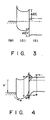
- Fig. 3 is a band diagram showing a thermal equilibrium state of the device of this embodiment.
- a junction which facilitates injection of holes from the metal electrode (M) 13 into the organic layer (O) 12 is formed between the electrode 13 and the layer 12.
- Fig. 4 is a band diagram showing a state in which a positive voltage V is applied to the metal electrode 13 of this luminescent device. Holes injected from the metal electrode 13 into the organic layer 12 upon application of the voltage are stored in a junction interface between the layer 12 and the semiconductor substrate 11, and electrons in the substrate 11 are also stored in the junction interface between the layer 12 and the substrate 11, thereby forming an electric double layer in the junction interface. Since the thickness of this electric double layer is a molecular size ( ⁇ 1 nm) of a dye, an electric field generated in this portion is about 107 V/cm accordingly. As a result, the stored carriers are easily tunnel-injected into an adjacent layer through the blocking contact.
- the holes injected into the n-type semiconductor substrate 11 are recombined with the electrons as major carriers in the substrate 11 to emit light. If the organic layer 12 is a luminescent layer, the electrons injected into the layer 12 are recombined with the holes as major carriers in the layer 12 to emit light. The emitted light is extracted through the semiconductor substrate 11.
- Fig. 5 is a sectional view showing a luminescent device according to another embodiment of the present invention using a p-type semiconductor substrate.
- an organic layer (O) 22 and a metal electrode (M) 23 as a second electrode are stacked on a p-type semiconductor substrate (S) 21 as a first electrode.
- an ohmic metal 24 having a light exit window 25 is formed on the lower surface of the substrate 21.
- Fig. 6 shows electrical characteristics of each portion of the luminescent device of this embodiment obtained before bonding.
- the conduction band level, the Fermi level, and the valence band level of the semiconductor substrate 21 are E CS , E FS , and E VS , respectively
- the conduction band level, the Fermi level, and the valence band level of the organic layer 22 are E CO , E FO , and E VO
- the work function of the metal electrode 23 is E M
- materials are so selected as to satisfy the following relations: E M ⁇ E FO E CO > E CS E FO > E FS E VO > E VS
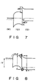
- Fig. 7 is a band diagram showing a thermal equilibrium state of the device of this embodiment.
- a junction which facilitates injection of electrons from the metal electrode (M) 23 into the organic layer (O) 22 is formed between the electrode 23 and the layer 22.
- Fig. 8 is a band diagram showing a state in which a negative voltage -V is applied to the metal electrode 23 of the luminescent device. Electrons injected from the metal electrode 23 into the organic layer 22 upon application of the voltage are stored in a junction interface between the layer 22 and the semiconductor substrate 21, and holes in the substrate 21 are also stored in the junction interface between the layer 22 and the substrate 21, thereby forming an electric double layer in the junction interface. As in the first embodiment, these carriers are tunnel-injected into an adjacent layer through the blocking contact and recombined to emit light in at least one of the semiconductor substrate 21 and the organic layer 22. The emitted light is extracted through the substrate 21.
- the device has a memory function in its luminescent characteristics.
- the memory function is obtained because the two types of carriers, i.e., electrons and holes are simultaneously injected into the organic layer. The reason for this will be described in more detail below.
- an organic material used in a luminescent device generally has a small carrier mobility of at most 10 ⁇ 3 cm/V ⁇ sec, electrons injected in the material form a space charge.
- a current flowing in the material is an ohmic current (proportional to a voltage) in a low electric field and is a space-charge limitation current (proportional to the square of a voltage) which is limited by an internal electric field in a high electric field. Therefore, no memory function can be obtained.
- an electron injection property is imparted to one of the electrodes sandwiching the organic film, and a hole injection property is imparted to the other electrode. When a bias is applied, therefore, electrons and holes are simultaneously injected and stored in the organic film.
- Fig. 9 shows a hysteresis characteristic of voltage V - current I obtained when the luminescent device of the present invention is constant-voltage-driven. Referring to Fig. 9, the current I on the ordinate corresponds to the luminosity of luminescence.
- Fig. 10 is a negative resistance characteristic of voltage V - current I obtained when the luminescent device of the present invention is constant-current-driven. Referring to Fig. 10, the current I on the ordinate corresponds to the luminosity of luminescence.
- a rectification characteristic as shown in Fig. 11 is obtained.
- a polarity which causes the metal electrode 13 to serve as a positive electrode corresponds to a forward direction.
- a forward current is flowed by tunnel injection obtained upon formation of the electric double layer. No current flows upon application of a reverse bias because no electrons are injected from the metal electrode 13 into the organic layer and the semiconductor substrate 11 is depleted.
- a triangular-wave AC bias is applied to the luminescent device to measure a displacement current.
- a measurement region is a small current region near the origin of the voltage-current characteristic as indicated by a broken line in Fig. 11.
- Fig. 12 shows the obtained displacement current characteristic.
- a reverse bias region i.e., on the left side of a point A in Fig. 12
- no carrier injection occurs in the organic film and a semiconductor near the junction portion is depleted as described above.
- a portion between the two electrodes serves as a capacitor sandwiching the organic layer as an insulator and the depletion layer of a semiconductor, and a capacitance C is small.
- the displacement current I is generally represented by the following equation with respect to the capacitance C:
- the capacitance C is small because it is a series capacitance of the capacitance of the organic layer and that of the semiconductor depletion layer. Therefore, the displacement current is small.
- the carrier injection and storage states of the device of this embodiment can be confirmed by measuring the displacement current characteristic of the device.
- the operation mechanism of the luminescent device according to the present invention has been described above.
- formation of the electric double layer required to cause tunnel injection is based on the electrical characteristics of the organic/inorganic semiconductor junction surface.
- a very thin insulating film free from pin holes e.g., about 1 nm or less, must be formed.
- the thickness of the organic layer can be 10 to 100 nm or more. Therefore, a problem of pin holes which is a fatal defect of the MIS luminescent device can be avoided in the present invention.
- the luminescent device shown in Fig. 1 satisfies the relation (9), electron injection from the semiconductor substrate into the organic layer occurs in an electric field lower than that of hole injection from the organic layer into the semiconductor substrate, and luminescence in the organic layer becomes dominant.
- the relation (9) indicates that the band gap of the semiconductor substrate is wider than that of the organic layer, the luminescence in the organic layer is not reabsorbed by the semiconductor substrate but externally extracted.
- the relation (10) is satisfied, the hole injection into the semiconductor substrate is prior to the electron injection, and luminescence in the semiconductor substrate becomes dominant. The luminescence in the semiconductor substrate is not shielded by the organic layer but externally extracted.
- luminescence having mixed colors can be obtained, and a one-pixel multicolor display device can be realized.
- condition of relation (9) long-wavelength luminescence is obtained in the organic layer upon application of a low voltage, and short-wavelength luminescence is additionally obtained in the semiconductor substrate upon application of a high voltage.
- the organic/inorganic semiconductor junction type luminescent device according to the present invention has an advantage of a longer life than that of a device using only an organic layer. This long life is obtained because many inorganic semiconductors have high thermal conductivities and therefore destruction of an organic film caused by Joule heat generated by a current flowing through the device is prevented.
- a device formation process was as follows. That is, a 100-nm thick thin bicoronenyl film was formed by a vacuum sublimation method (vacuum degree ⁇ 10 ⁇ 6 Torr) on an n-type GaP substrate having a donut-like AuGe electrode formed on its lower surface by vacuum deposition, and a 50-nm thick Au electrode was formed thereon by the vacuum deposition method.
- a device formation process was as the same as that of Experimental Example 1.
- a bias was applied by using the Au electrode as an anode, a current of 50 mA/cm2 flowed at an application voltage of 5 V, and green luminescence having a luminosity of 500 Cd/m2 was obtained.
- a device formation process was as follows. That is, a 100-nm thick bicoronenyl derivative film was formed by a vacuum sublimation method on an n-type ZnS substrate having a donut-like InGa electrode formed on its lower surface, and an Au electrode was formed thereon by a vacuum deposition method.
- a device formation process was the same as in Experimental Example 1. When a positive bias was applied to the Au electrode, green luminescence was obtained from the organic layer.
- Fig. 13 shows hysteresis characteristics obtained by constant-voltage-driving the luminescent device of the experimental example.
- Fig. 14 shows negative resistance characteristics obtained by constant-current-driving the device.
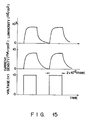
- Fig. 15 shows afterimage characteristics obtained by pulse-driving the device.
- the luminescent device of this experimental example has a memory function in its luminescent characteristics.
- An average luminous efficacy of the device was about 10%, and its life reached 100,000 hours.
- a device formation process was the same as that in Experimental Example 1. When a bias was applied by using the Au electrode as an anode, a current of 50 mA/cm2 flowed at an application voltage of 5 V, and green luminescence having a luminosity of 500 Cd/cm2 was obtained.
- An average luminous efficacy of the device was about 10%, and its life reached 100,000 hours.
- An embodiment in which the present invention is applied to a field-effect device will be described below.
- An FET having excellent characteristics can be obtained by applying an organic/inorganic semiconductor junction of a luminescent device and the principle of formation of an electric double layer utilizing injection of electrons and holes to a gate portion.
- an FET not only a compound semiconductor but also Si and the like can be used.
- An organic layer has a large number of types and a wide range of positions of a conduction band, a Fermi level, and a valence band as a semiconductor as compared with an inorganic semiconductor. In order to realize a heterojunction, a lattice constant is strictly limited in an inorganic semiconductor.
- a dye molecule Since, however, a dye molecule has an electron structure of a closed shell type, it does not have a so-called dangling bond on its surface and therefore can be freely bonded with another material. For these reasons, by using an organic/inorganic semi-conductor junction, a good heterojunction which cannot be obtained by using only an inorganic semiconductor can be easily realized.
- Fig. 16 is an embodiment of a p-channel FET using an n-type inorganic semiconductor substrate.
- a p-type source layer 32 and a p-type drain layer 33 are formed to be separated from each other on an n-type semiconductor substrate (S) 31.
- a gate electrode 35 is formed between the source layer 32 and the drain layer 33 of the substrate 31 via an organic layer (O) 34.
- Fig. 17 shows electrical characteristics of gate electrode (M)-organic layer (O)-semiconductor substrate (S) of the FET of this embodiment obtained before bonding. That is, assuming that the conduction band level, the Fermi level, and the valence band level of the semiconductor substrate 31 are E CS , E FS , and E VS , respectively, the conduction band level, the Fermi level, and the valence band level of the organic layer 34 are E CO , E FO , and E VO , respectively, and the work function of the gate electrode 35 is E M , materials are so selected as to satisfy the following relations: E CO > E CS E VO > E VS E M ⁇ E FO
- Fig. 18 is a band diagram showing a thermal equilibrium state of the gate portion of an FET which satisfies the above conditions.
- the organic layer 34 has an electron injection property.
- a blocking barrier is formed in the conduction band against electrons injected from the layer 34 into the substrate 31, and a blocking barrier is formed in the valence band against holes injected from the substrate 31 into the layer 34. Therefore, en electric double layer is formed in the junction portion between the organic layer 34 and the semiconductor substrate 31.
- a p-type inversion layer is formed on the surface of the substrate 31. Therefore, this device is of a depletion type FET.
- an electric field intensity applied on a channel depends on the thickness of a gate insulating film and is about 105 V/cm in a normal operation.
- an electric field intensity of about 107 V/cm is easily obtained. That is, since a large drain current can be controlled by a small gate voltage, a high transconductance gm is obtained.
- an enhancement type FET can be easily obtained by selecting a combination of the materials of the organic layer 34 and the gate electrode 35.
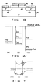
- Fig. 19 shows an embodiment of an n-channel FET.
- an n-type source layer 42 and an n-type drain layer 43 are formed to be separated from each other on a p-type semiconductor substrate 41, and a gate electrode 45 is formed on the surface of the substrate between the layers 42 and 43 via an organic layer 44.
- Fig. 20 shows electrical characteristics of gate electrode (M)-organic layer (O)-semiconductor substrate (S) of the FET of this embodiment obtained before bonding.
- materials are so selected as to satisfy the following relations: E CO ⁇ E CS E VO ⁇ E VS E M > E FO
- Fig. 21 is a band diagram showing a thermal equilibrium state of the gate portion of the FET of this embodiment.
- the organic layer 44 has a hole injection property.
- a blocking barrier is formed in the conduction band against injection of electrons from the substrate 41 into the layer 44, and a blocking barrier is formed in the valence band against injection of holes from the layer 44 into the substrate 41.
- An electric double layer is formed in the junction portion between the organic layer 44 and the semiconductor substrate 41, and an n-type inversion layer is formed on the surface of the substrate 41.
- either a depletion type or enhancement type FET can be obtained by selecting the materials of the gate electrode 45 and the organic layer 44.
- the organic layer causes a structural change to fixedly trap the injected electrons, as shown in Fig. 22C. Even after the gate bias is removed, therefore, the electrons are kept trapped in the organic layer, as shown in Fig. 22D, to keep the ON state of the device. A certain period of time is required before the trapping caused by this structural change is canceled. Therefore, a memory characteristic is obtained.
- an aromatic imide dye may be used as the organic layer.
- an insulating film consisting of an organic polymeric material or an inorganic material such as SiO2 may be formed between the gate electrode and the organic layer. This structure can be effectively used to form an enhancement type FET having a high threshold value.
- n-type semiconductor substrate 31 n-type Si organic layer 34: gate electrode 35: Au were used.
- a device formation process was as follows. P-type source and drain layers were formed by ion implantation into an n-type Si substrate, and source and drain electrodes were formed by depositing and patterning an Al film. Thereafter, a 50-nm thick organic layer was formed across the source and drain regions by a vacuum sublimation method (vacuum degree ⁇ 10 ⁇ 6 Torr), and an Au gate electrode was formed thereon.
- the obtained device was in an OFF state at a gate voltage of 0 V and was turned on upon application of a negative gate voltage.
- the device was kept in the ON state for a predetermined time period after the gate voltage was returned to 0 V.
- p-type semiconductor substrate 41 p-type Si organic layer 44: tetra(paraisopropylphenyl)benzidine gate electrode 45: Au were used.
- a manufacturing process was basically the same as that in Experimental Example 6.
- the obtained FET had a very high gm. That is, the FET of this example had a gm about 100 times that of a MOSFET having the same gate length and gate width and using a 50-nm thick SiO2 film as a gate insulating film.
Landscapes
- Chemical & Material Sciences (AREA)
- Engineering & Computer Science (AREA)
- Materials Engineering (AREA)
- Organic Chemistry (AREA)
- Inorganic Chemistry (AREA)
- Physics & Mathematics (AREA)
- Optics & Photonics (AREA)
- Led Devices (AREA)
- Electroluminescent Light Sources (AREA)
- Insulated Gate Type Field-Effect Transistor (AREA)
Applications Claiming Priority (2)
| Application Number | Priority Date | Filing Date | Title |
|---|---|---|---|
| JP61526/90 | 1990-03-13 | ||
| JP2061526A JPH03262170A (ja) | 1990-03-13 | 1990-03-13 | 有機/無機接合型半導体素子 |
Publications (2)
| Publication Number | Publication Date |
|---|---|
| EP0448268A2 true EP0448268A2 (fr) | 1991-09-25 |
| EP0448268A3 EP0448268A3 (en) | 1992-12-02 |
Family
ID=13173634
Family Applications (1)
| Application Number | Title | Priority Date | Filing Date |
|---|---|---|---|
| EP19910302038 Withdrawn EP0448268A3 (en) | 1990-03-13 | 1991-03-12 | Semiconductor luminescent device having organic/inorganic junction |
Country Status (3)
| Country | Link |
|---|---|
| US (1) | US5105233A (fr) |
| EP (1) | EP0448268A3 (fr) |
| JP (1) | JPH03262170A (fr) |
Cited By (6)
| Publication number | Priority date | Publication date | Assignee | Title |
|---|---|---|---|---|
| WO1997047051A1 (fr) * | 1996-06-05 | 1997-12-11 | International Business Machines Corporation | Anodes au nitrure de gallium pour affichages et dispositifs organiques electroluminescents |
| WO1998007202A1 (fr) * | 1996-08-08 | 1998-02-19 | International Business Machines Corporation | Cathodes en nitrure de gallium pour dispositifs electroluminescents et ecrans de visualisation |
| EP0856896A1 (fr) * | 1997-02-04 | 1998-08-05 | International Business Machines Corporation | Diode émettrice de lumière |
| WO2004003972A3 (fr) * | 2002-07-01 | 2004-07-08 | Hewlett Packard Development Co | Transistor et detecteurs fabriques dans des materiaux moleculaires a dipoles electriques |
| EP1406127A3 (fr) * | 2002-09-30 | 2005-02-02 | Samsung Electronics Co., Ltd. | Organophotorécepteur comprenant un composé contenant un groupe de toluidine |
| CN106632085A (zh) * | 2016-12-23 | 2017-05-10 | 长春海谱润斯科技有限公司 | 一种含氮杂环衍生物及使用该含氮杂环衍生物的有机发光器件 |
Families Citing this family (13)
| Publication number | Priority date | Publication date | Assignee | Title |
|---|---|---|---|---|
| US5343050A (en) * | 1992-01-07 | 1994-08-30 | Kabushiki Kaisha Toshiba | Organic electroluminescent device with low barrier height |
| JP2821347B2 (ja) * | 1993-10-12 | 1998-11-05 | 日本電気株式会社 | 電流制御型発光素子アレイ |
| JPH08102360A (ja) * | 1994-09-29 | 1996-04-16 | Toyota Central Res & Dev Lab Inc | 有機無機複合薄膜型電界発光素子 |
| US6123130A (en) * | 1997-11-11 | 2000-09-26 | Bridgestone/Firestone, Inc. | Tire having improved wet stopping capability |
| EP1111967A1 (fr) * | 1999-04-30 | 2001-06-27 | Idemitsu Kosan Co., Ltd. | Dispositif organique electroluminescent et procede de fabrication |
| KR100657891B1 (ko) * | 2003-07-19 | 2006-12-14 | 삼성전자주식회사 | 반도체 나노결정 및 그 제조방법 |
| WO2005053002A2 (fr) * | 2003-11-25 | 2005-06-09 | Princeton University | Element de memoire a jonction de redressement et a deux composants |
| JP4764085B2 (ja) * | 2005-07-22 | 2011-08-31 | 株式会社ブリヂストン | 空気入りタイヤ |
| JP2008124360A (ja) * | 2006-11-15 | 2008-05-29 | Sony Corp | 機能性分子素子及びその製造方法、並びに機能性分子装置 |
| JP5149389B2 (ja) * | 2007-09-18 | 2013-02-20 | クワンジュ インスティチュート オブ サイエンス アンド テクノロジー | 酸化還元反応を用いる有機−無機ハイブリッド型接合素子およびこれを用いる有機太陽電池 |
| JP4825817B2 (ja) * | 2008-01-18 | 2011-11-30 | 三井化学株式会社 | トリフェニルメタン誘導体、およびそれを含む有機電界発光素子 |
| TWI602901B (zh) * | 2012-12-11 | 2017-10-21 | 半導體能源研究所股份有限公司 | 發光元件,發光裝置,電子裝置,與照明裝置 |
| JP2018160548A (ja) | 2017-03-22 | 2018-10-11 | 東芝メモリ株式会社 | 記憶装置及び整流装置 |
Family Cites Families (8)
| Publication number | Priority date | Publication date | Assignee | Title |
|---|---|---|---|---|
| JPS604276A (ja) * | 1983-06-22 | 1985-01-10 | Nec Corp | 発光素子 |
| GB8406691D0 (en) * | 1984-03-14 | 1984-04-18 | Secr Defence | Electroluminescent devices |
| EP0195395B1 (fr) * | 1985-03-22 | 1989-12-13 | Kanegafuchi Kagaku Kogyo Kabushiki Kaisha | Dispositif électroluminescent |
| EP0218422B1 (fr) * | 1985-09-30 | 1992-09-16 | Kabushiki Kaisha Toshiba | Elément photoémetteur à semi-conducteur |
| JP2581165B2 (ja) * | 1988-06-09 | 1997-02-12 | 日本電気株式会社 | 有機薄膜el素子 |
| JP2636341B2 (ja) * | 1988-06-09 | 1997-07-30 | 日本電気株式会社 | 有機薄膜el素子 |
| US5200668A (en) * | 1988-11-21 | 1993-04-06 | Mitsui Toatsu Chemicals, Inc. | Luminescence element |
| US5006915A (en) * | 1989-02-14 | 1991-04-09 | Ricoh Company, Ltd. | Electric device and photoelectric conversion device comprising the same |
-
1990
- 1990-03-13 JP JP2061526A patent/JPH03262170A/ja active Pending
-
1991
- 1991-03-12 EP EP19910302038 patent/EP0448268A3/en not_active Withdrawn
- 1991-03-13 US US07/669,020 patent/US5105233A/en not_active Expired - Lifetime
Cited By (10)
| Publication number | Priority date | Publication date | Assignee | Title |
|---|---|---|---|---|
| WO1997047051A1 (fr) * | 1996-06-05 | 1997-12-11 | International Business Machines Corporation | Anodes au nitrure de gallium pour affichages et dispositifs organiques electroluminescents |
| WO1997047050A1 (fr) * | 1996-06-05 | 1997-12-11 | International Business Machines Corporation | Semi-conducteurs non degeneres a bande interdite large et/ou electrodes de contact pour dispositifs organiques electroluminescents |
| KR100324869B1 (ko) * | 1996-06-05 | 2002-05-09 | 포만 제프리 엘 | 유기발광디바이스및디스플레이 |
| US6433355B1 (en) * | 1996-06-05 | 2002-08-13 | International Business Machines Corporation | Non-degenerate wide bandgap semiconductors as injection layers and/or contact electrodes for organic electroluminescent devices |
| WO1998007202A1 (fr) * | 1996-08-08 | 1998-02-19 | International Business Machines Corporation | Cathodes en nitrure de gallium pour dispositifs electroluminescents et ecrans de visualisation |
| EP0856896A1 (fr) * | 1997-02-04 | 1998-08-05 | International Business Machines Corporation | Diode émettrice de lumière |
| WO2004003972A3 (fr) * | 2002-07-01 | 2004-07-08 | Hewlett Packard Development Co | Transistor et detecteurs fabriques dans des materiaux moleculaires a dipoles electriques |
| US7186380B2 (en) | 2002-07-01 | 2007-03-06 | Hewlett-Packard Development Company, L.P. | Transistor and sensors made from molecular materials with electric dipoles |
| EP1406127A3 (fr) * | 2002-09-30 | 2005-02-02 | Samsung Electronics Co., Ltd. | Organophotorécepteur comprenant un composé contenant un groupe de toluidine |
| CN106632085A (zh) * | 2016-12-23 | 2017-05-10 | 长春海谱润斯科技有限公司 | 一种含氮杂环衍生物及使用该含氮杂环衍生物的有机发光器件 |
Also Published As
| Publication number | Publication date |
|---|---|
| EP0448268A3 (en) | 1992-12-02 |
| US5105233A (en) | 1992-04-14 |
| JPH03262170A (ja) | 1991-11-21 |
Similar Documents
| Publication | Publication Date | Title |
|---|---|---|
| US5105233A (en) | Semiconductor luminescent device having organic/inorganic junction | |
| EP0498979B1 (fr) | Dispositif électroluminescent organique | |
| Era et al. | Organic‐inorganic heterostructure electroluminescent device using a layered perovskite semiconductor (C6H5C2H4NH3) 2PbI4 | |
| Takahashi et al. | Ambipolar light‐emitting transistors of a tetracene single crystal | |
| US5294810A (en) | Organic electroluminescent device | |
| JPH04297076A (ja) | 有機el素子 | |
| JPH0765958A (ja) | 有機el素子 | |
| KR102674794B1 (ko) | 양자점 발광다이오드, 그 제조 방법 및 양자점 발광표시장치 | |
| JP2636341B2 (ja) | 有機薄膜el素子 | |
| EP0398764B1 (fr) | Dispositif électroluminescent à couche mince organique | |
| JP3237905B2 (ja) | 有機el素子 | |
| US20210388261A1 (en) | Perovskite lighting systems | |
| US3492548A (en) | Electroluminescent device and method of operating | |
| JPWO2006025274A1 (ja) | 有機半導体発光装置およびそれを用いた表示装置 | |
| JP2991450B2 (ja) | 有機膜発光素子 | |
| JP2581165B2 (ja) | 有機薄膜el素子 | |
| Fischer | Electroluminescent II–VI Heterojunctions | |
| US4893154A (en) | Electroluminescent device | |
| Allen | Electroluminescence in reverse-biassed Schottky diodes | |
| Hosokawa et al. | 31.3: Organic EL Materials Based on Styryl and Amine Derivatives | |
| KR102690691B1 (ko) | 양자점 발광다이오드 및 이를 포함하는 양자점 발광표시장치 | |
| JPH02207488A (ja) | 薄膜型発光素子 | |
| US4161814A (en) | Tunnel injection of minority carriers in semi-conductors | |
| JP2658687B2 (ja) | 有機薄膜el素子 | |
| JPH0210693A (ja) | 有機薄膜el素子 |
Legal Events
| Date | Code | Title | Description |
|---|---|---|---|
| PUAI | Public reference made under article 153(3) epc to a published international application that has entered the european phase |
Free format text: ORIGINAL CODE: 0009012 |
|
| 17P | Request for examination filed |
Effective date: 19910327 |
|
| AK | Designated contracting states |
Kind code of ref document: A2 Designated state(s): DE FR GB |
|
| PUAL | Search report despatched |
Free format text: ORIGINAL CODE: 0009013 |
|
| AK | Designated contracting states |
Kind code of ref document: A3 Designated state(s): DE FR GB |
|
| 17Q | First examination report despatched |
Effective date: 19930201 |
|
| STAA | Information on the status of an ep patent application or granted ep patent |
Free format text: STATUS: THE APPLICATION IS DEEMED TO BE WITHDRAWN |
|
| 18D | Application deemed to be withdrawn |
Effective date: 19930612 |