EP0448624B1 - Busschnittstellensteuerung für rechnergrafiken - Google Patents
Busschnittstellensteuerung für rechnergrafiken Download PDFInfo
- Publication number
- EP0448624B1 EP0448624B1 EP90901134A EP90901134A EP0448624B1 EP 0448624 B1 EP0448624 B1 EP 0448624B1 EP 90901134 A EP90901134 A EP 90901134A EP 90901134 A EP90901134 A EP 90901134A EP 0448624 B1 EP0448624 B1 EP 0448624B1
- Authority
- EP
- European Patent Office
- Prior art keywords
- output
- multiplexer
- input
- controller according
- cnt
- Prior art date
- Legal status (The legal status is an assumption and is not a legal conclusion. Google has not performed a legal analysis and makes no representation as to the accuracy of the status listed.)
- Expired - Lifetime
Links
Images
Classifications
-
- G—PHYSICS
- G06—COMPUTING OR CALCULATING; COUNTING
- G06F—ELECTRIC DIGITAL DATA PROCESSING
- G06F13/00—Interconnection of, or transfer of information or other signals between, memories, input/output devices or central processing units
- G06F13/10—Program control for peripheral devices
- G06F13/12—Program control for peripheral devices using hardware independent of the central processor, e.g. channel or peripheral processor
- G06F13/122—Program control for peripheral devices using hardware independent of the central processor, e.g. channel or peripheral processor where hardware performs an I/O function other than control of data transfer
Definitions
- the invention is directed generally to the field of digital information systems and, more particularly, to a bus interface controller apparatus for use in computer graphics systems.
- Some examples of known memory interface chips include the 373/374 latch or 244/245 buffer/transceiver.
- Texas Instruments, Inc. has produced a crossbar switch Model No. 74AS8840 which includes 64 I/O pins arranged in 16 4-bit groups, where each group of four pins serves as a bi-directional input to an output from a 4-bit multiplexer.
- devices such as AMD Company's Model No. Am29C98 which is a 9-bit by four port multiple bus exchange device. Typical port-to-port delays for such devices are in the 9 to 10 nanosecond range. Such devices also require a large amount of external user-supplied control logic relative to the interface device of the invention.
- the invention has advantages over the known devices of the prior art including internal latching buffering architecture which is user configurable, via output configuration control lines.
- the invention provides the speed necessary with TTL/CMOS compatible inputs and outputs.
- a bus interface controller for use in a digital information system having a system clock is set forth in Claim 1.
- the bus interface controller comprises more than four data channels of more than nine bits per channel which feed into apparatus for multiplexing the data channels bi-directionally so as to accomplish routing of data from any channel to any or all of the remaining channels.
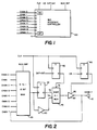
- Figure 1 shows a block diagram of an illustrative example of the bus interface controller device of the invention having a clock line, eight output control lines (Out-Cnt), eight output enable lines (OE), and twenty-four multiplexer control lines (Mux-Cnt) as well as eight 16-bit data channels Chan 0 - Chan 7.
- Figure 2 shows a detailed design of an illustrative embodiment of the bus interface controller chip of the invention.
- FIG. 1 shows a block diagram of an illustrative example of the bus interface controller device of the invention 100.
- the device 100 has a plurality of input/output (I/O) ports including channels Chan 0 through Chan 7. These channels are, in one example of the device, 16-bit bi-directional bus lines.
- user configurable control inputs including the clock input (CLK), the output enable input (OE), the output control input (Out-Cnt) and the multiplexer control input (MUX-CNT).
- CLK clock input
- OE output enable input
- Out-Cnt the output control input
- MUX-CNT multiplexer control input
- input CLK will be a single line routed throughout the chip carrying the clocking signal.
- bus interface controller 100 are eight identically replicated circuits, one for each of the eight channels in this example. If more or less channels are used, the replicated circuits will vary accordingly. These circuits are discussed in more detail below with reference to Figure 2.
- the OE line and Out-Cnt lines are each 8-bits wide and used for controlling each of the eight replicated circuits within the bus interface controller.
- the MUX-CNT lines are advantageously 24-bits wide, using 3 bits to control each of 8 multiplexer circuits as contained within the replicated circuits A0 through A7.
- FIG. 2 shows a functional block diagram of an illustrative embodiment of the invention.
- the bus interface controller of the invention comprises a circuit as shown in Figure 2 replicated into identical circuits A0 - A7 for each channel.
- the example shown in Figure 2 is the circuit block for Chan 7 including I/O port 10 for Chan 7 which feeds back to the channel 7 input of multiplexer 20.
- a similar block exists within the bus interface controller chip for each of the remaining channels 0 through 6.
- the circuit block A6 for chan 6 will have the I/O port for Chan 6 fed back into the Chan 6 input for the A6 multiplexer and the other channels will be cross-fed into Chan 6 through their designated multiplexer inputs.
- a circuit as shown in Figure 2, corresponding to each of the channels used by the bus interface controller of the invention wherein the only variable is the channel designation for the I/O port.
- a first latch or flip-flop 30 is shown having a clock input and a D-input connected to the output of the multiplexer 20.
- Flip-flop 30 has a Q-output.
- Buffer 40 is also connected to the output of the multiplexer 20 and the D-input of flip-flop 30.
- a second flip-flop 50 also has a clocking input and an output control input (Out-Cnt) and a Q-output.
- a third flip-flop 60 has an output enable input (OE), a clocking input and a Q-output.
- the apparatus of the invention further comprises a second multiplexer having first and second inputs and an output and a control input 70. The first input 72 is connected to the Q-output of flip-flop 30.
- the second input 74 is connected to the output of buffer 40.
- the second latch 50 has its output connected to the control input of the multiplexer 70 at 76.
- the output of multiplexer 70 is connected to the input of buffer 80.
- Buffer 80 has a control input 82 connected to the output of latch 60.
- the output of buffer 80 is connected to the input 10 of channel 7 which is further feedback to the channel input of the first multiplexer 20.
- Multiplexer 20 has a control input MUX-CNT which is preferably a 3-bit control line for a 16-bit, eight channel device as shown in Figure 2 by way of illustration and not by way of limitation.
- the design of the invention may be embodied in a semi-conductor material preferably comprised of gallium arsenide.
- a bus interface controller comprised of eight 16-bit, bi-directional buses will have a power dissipation of less than 500 milliwatts. Such a system will operate at 26 MHz and above with less than a four nanosecond propagation delay.
- the output drives of such a system will preferably be in the range of six to eight milliamps.
- Inputs and outputs will be TTL/CMOS compatible with tri-state outputs.
- the latch/buffer architecture can be user-configurable.
- data may be introduced onto channels Chan 0 through Chan 7 through the I/O ports such as input 10 as shown in Figure 2.
- the multiplexer 20 for each channel selects the data to be throughput in accordance with the 3-bit control signal on line MUX-CNT. For example, if the bits appearing on MUX-CNT during a control cycle read "001", channel 1 would be switched onto the output of multiplexer 20.
- the latches 30, 50 and 60 together with multiplexer 70 determine which direction the data is flowing, in or out. If latch 60 receives an output enable signal, it is passed on the next control clock cycle to enable data to flow through buffer 80. If buffer 80 is disabled through the operation of flip-flop 60, data can flow into the channel, in this case, channel 7, from elsewhere in the digital system, such as a user input. Similarly, multiplexer 70 is controlled by latch 50 and determines whether data will flow into the I/O port 10 through latch 30 or through buffer 40 from multiplexer 20. Each of the channels operates in a similar manner.
Landscapes
- Engineering & Computer Science (AREA)
- Theoretical Computer Science (AREA)
- Physics & Mathematics (AREA)
- General Engineering & Computer Science (AREA)
- General Physics & Mathematics (AREA)
- Information Transfer Systems (AREA)
- Bus Control (AREA)
Claims (9)
- Bus-Schnittstellensteuerung (100) zur Verwendung in einem digitalen Informationssystem mit einem Systemtakt, gekennzeichnet durch eine Einrichtung (CLK,OE,OUT-CNT,MUX-CNT) zum Steuern des Datenflusses;
mehr als vier Datenkanäle (CHAN0-CHAN7) mit jeweils mehr als 9 Bit;
mehrere Multiplexerschaltkreise, wobei jeweils ein Multiplexerschaltkreis für jeden Kanal vorgesehen ist und jeder Multiplexerschaltkreis umfaßt einen ersten Multiplexer (20) mit einem Ausgang und mehreren Eingängen, deren Anzahl wenigstens der Anzahl der Kanäle entspricht;
eine erste Verriegelung (30) mit einem an den Ausgang des Multiplexers (20) an einem ersten Knoten angeschlossenen Eingang und einem Ausgang; einen ersten Puffer (40) mit einem an den ersten Knoten angeschlossenen Eingang und einem Ausgang; eine zweite Verriegelung (50) mit einem Ausgang-Steuereingang und einem Ausgang;
einen zweiten Multiplexer (70), der mit einem ersten Eingang an den Ausgang des ersten Puffers (40) und mit einem zweiten Eingang an den Ausgang der ersten Verriegelung (30) sowie mit einem Steuereingang an den Ausgang der zweiten Verriegelung (50) angeschlossen ist und ferner einen Ausgang aufweist; eine dritte Verriegelung (60) mit einem Ausgang-Freigabeeingang und einem Ausgang; und
einen zweiten Puffer (80), der mit einem Eingang an den Ausgang des zweiten Multiplexers (70) und mit einem Steuereingang an den Ausgang der dritten Verriegelung (60) angeschlossen ist und der einen Ausgang aufweist, der an einen Ein/Ausgabe-Anschluß (10) und den entsprechenden Kanaleingang des ersten Multiplexers (20) angeschlossen ist. - Steuerung nach Anspruch 1, dadurch gekennzeichnet, daß der erste Multiplexer (20) ein 8 aus 1-Codierer ist.
- Steuerung nach Anspruch 1, dadurch gekennzeichnet, daß der zweite Multiplexer (70) ein 2 aus 1-Codierer ist.
- Steuerung nach Anspruch 1, dadurch gekennzeichnet, daß die Verriegelungen (30,50,60) D-Flip-Flop-Schaltkreise umfassen.
- Steuerung nach Anspruch 1, dadurch gekennzeichnet, daß sie in ein Halbleitermaterial aus Gallium-Arsenid eingebettet ist.
- Steuerung nach Anspruch 1, dadurch gekennzeichnet, daß die Datenkanäle Dreistufen-Ausgänge umfassen.
- Steuerung nach Anspruch 1, gekennzeichnet durch Ein/Ausgangsleitungen, welche TTL/CMOS-kompatibel sind.
- Steuerung nach Anspruch 1, dadurch gekennzeichnet, daß die Steuereinrichtung umfaßt:
Eine System-Taktleitung (CLK);
mehrere Ausgang-Freigabeleitungen (OE);
mehrere Ausgang-Steuerleitungen (OUT-CNT); und
mehrere Multiplexer-Steuerleitungen (MUX-CNT). - Steuerung nach einem der Ansprüche 1 bis 7,
gekennzeichnet durch:
Eine System-Taktleitung (CLK);
wenigstens acht Ausgang-Freigabeleitungen (OE);
wenigstens acht bidirektionale Kanäle (CHAN0-CHAN7) mit jeweils wenigstens 16 Bit;
Einrichtungen (20-80) zum Multiplexen der bidirektionalen Datenkanäle, um eine Datenverzweigung von irgendeinem Kanal zu irgendeinem oder allen anderen Kanälen zu bewerkstelligen;
wenigstens acht Ausgang-Steuerleitungen (OUT-CNT), die so konfiguriert sind, um die Übertragung der Verzweigungdaten von der Multiplexereinrichtung zu steuern; und
wenigstens 24 Multiplexer-Steuerleitungen (MUX-CNT), die so konfiguriert sind, daß sie den Datenkanal auswählen, auf den durch die Multiplexereinrichtung verzweigt wird.
Applications Claiming Priority (2)
| Application Number | Priority Date | Filing Date | Title |
|---|---|---|---|
| US07/287,100 US5070449A (en) | 1988-12-19 | 1988-12-19 | Bus interface controller for computer graphics |
| US287100 | 1988-12-19 |
Publications (2)
| Publication Number | Publication Date |
|---|---|
| EP0448624A1 EP0448624A1 (de) | 1991-10-02 |
| EP0448624B1 true EP0448624B1 (de) | 1994-03-30 |
Family
ID=23101446
Family Applications (1)
| Application Number | Title | Priority Date | Filing Date |
|---|---|---|---|
| EP90901134A Expired - Lifetime EP0448624B1 (de) | 1988-12-19 | 1989-11-13 | Busschnittstellensteuerung für rechnergrafiken |
Country Status (6)
| Country | Link |
|---|---|
| US (1) | US5070449A (de) |
| EP (1) | EP0448624B1 (de) |
| JP (1) | JP2952521B2 (de) |
| CA (1) | CA2003554A1 (de) |
| DE (1) | DE68914289T2 (de) |
| WO (1) | WO1990007156A1 (de) |
Families Citing this family (9)
| Publication number | Priority date | Publication date | Assignee | Title |
|---|---|---|---|---|
| GB2246683A (en) * | 1990-06-22 | 1992-02-05 | Rank Cintel Ltd | Digital video data routing apparatus |
| GB9018992D0 (en) * | 1990-08-31 | 1990-10-17 | Ncr Co | Internal bus for work station interfacing means |
| US5379386A (en) * | 1991-09-05 | 1995-01-03 | International Business Machines Corp. | Micro channel interface controller |
| US5428797A (en) * | 1991-12-23 | 1995-06-27 | Apple Computer, Inc. | Circuitry for eliminating bus contention at high frequencies by driving a bus to an available state prior to its relinquishing control of the bus |
| US5426739A (en) * | 1992-03-16 | 1995-06-20 | Opti, Inc. | Local bus - I/O Bus Computer Architecture |
| US5309568A (en) * | 1992-03-16 | 1994-05-03 | Opti, Inc. | Local bus design |
| US5463658A (en) * | 1994-03-23 | 1995-10-31 | Intel Corporation | Low impact collision detection method |
| US5596765A (en) * | 1994-10-19 | 1997-01-21 | Advanced Micro Devices, Inc. | Integrated processor including a device for multiplexing external pin signals |
| CN104348889B (zh) * | 2013-08-09 | 2019-04-16 | 鸿富锦精密工业(深圳)有限公司 | 切换开关及电子装置 |
Family Cites Families (7)
| Publication number | Priority date | Publication date | Assignee | Title |
|---|---|---|---|---|
| US4214213A (en) * | 1977-10-25 | 1980-07-22 | Rca Corporation | Signal selecting system |
| US4471456A (en) * | 1980-04-14 | 1984-09-11 | Sperry Corporation | Multifunction network |
| US4404556A (en) * | 1981-11-25 | 1983-09-13 | Western Electric Company, Inc. | Bit expansion circuit |
| US4717912A (en) * | 1982-10-07 | 1988-01-05 | Advanced Micro Devices, Inc. | Apparatus for producing any one of a plurality of signals at a single output |
| DE3247834A1 (de) * | 1982-12-23 | 1984-06-28 | Siemens AG, 1000 Berlin und 8000 München | Schaltkreis-baustein |
| US4761647A (en) * | 1987-04-06 | 1988-08-02 | Intel Corporation | Eprom controlled tri-port transceiver |
| US4852083A (en) * | 1987-06-22 | 1989-07-25 | Texas Instruments Incorporated | Digital crossbar switch |
-
1988
- 1988-12-19 US US07/287,100 patent/US5070449A/en not_active Expired - Lifetime
-
1989
- 1989-11-13 WO PCT/US1989/004970 patent/WO1990007156A1/en not_active Ceased
- 1989-11-13 JP JP2501199A patent/JP2952521B2/ja not_active Expired - Fee Related
- 1989-11-13 DE DE68914289T patent/DE68914289T2/de not_active Expired - Fee Related
- 1989-11-13 EP EP90901134A patent/EP0448624B1/de not_active Expired - Lifetime
- 1989-11-22 CA CA002003554A patent/CA2003554A1/en not_active Abandoned
Also Published As
| Publication number | Publication date |
|---|---|
| US5070449A (en) | 1991-12-03 |
| DE68914289D1 (de) | 1994-05-05 |
| EP0448624A1 (de) | 1991-10-02 |
| WO1990007156A1 (en) | 1990-06-28 |
| DE68914289T2 (de) | 1994-08-25 |
| CA2003554A1 (en) | 1990-06-19 |
| JP2952521B2 (ja) | 1999-09-27 |
| JPH04502378A (ja) | 1992-04-23 |
Similar Documents
| Publication | Publication Date | Title |
|---|---|---|
| US5418911A (en) | Data path switch method and apparatus that provides capacitive load isolation | |
| US5208491A (en) | Field programmable gate array | |
| US5625780A (en) | Programmable backplane for buffering and routing bi-directional signals between terminals of printed circuit boards | |
| US6049225A (en) | Input/output interface circuitry for programmable logic array integrated circuit devices | |
| US5136188A (en) | Input/output macrocell for programmable logic device | |
| US6278291B1 (en) | Programmable logic array devices with interconnect lines of various lengths | |
| EP0448624B1 (de) | Busschnittstellensteuerung für rechnergrafiken | |
| KR100326207B1 (ko) | 병렬버스를 통한 디지털 데이터 전송률을 증가시키는 방법 및 회로 | |
| US6888376B1 (en) | Multiple data rates in programmable logic device serial interface | |
| US6218864B1 (en) | Structure and method for generating a clock enable signal in a PLD | |
| US4851717A (en) | Master slice integrated circuit capable of high speed operation | |
| EP0363086B1 (de) | Masken-programmierbares Bussteuerungsgattenfeld | |
| US4894563A (en) | Output macrocell for programmable logic device | |
| JPH0711787B2 (ja) | デ−タ処理装置 | |
| US6225823B1 (en) | Input/output circuitry for programmable logic devices | |
| EP0674411A1 (de) | Virtueller Verbindungsspeicher spezial für Kommunikation zwischen Endgeräten die auf unterschiedlichen Geschwindigkeiten funktionieren | |
| US6031767A (en) | Integrated circuit I/O interface that uses excess data I/O pin bandwidth to input control signals or output status information | |
| US7350013B2 (en) | Bus communication apparatus for programmable logic devices and associated methods | |
| Akata et al. | A 250-Mb/s 32* 32 CMOS crosspoint LSI for ATM switching systems | |
| JPS6095940A (ja) | 多重路信号分配システム | |
| US6429681B1 (en) | Programmable logic device routing architecture to facilitate register re-timing | |
| US6304933B1 (en) | Method and apparatus for transmitting data on a bus | |
| US6904062B1 (en) | Method and apparatus for efficient and flexible routing between multiple high bit-width endpoints | |
| US7328361B2 (en) | Digital bus synchronizer for generating read reset signal | |
| EP0929042B1 (de) | Bussteuerung in einem Datenprozessor |
Legal Events
| Date | Code | Title | Description |
|---|---|---|---|
| PUAI | Public reference made under article 153(3) epc to a published international application that has entered the european phase |
Free format text: ORIGINAL CODE: 0009012 |
|
| 17P | Request for examination filed |
Effective date: 19910619 |
|
| AK | Designated contracting states |
Kind code of ref document: A1 Designated state(s): DE FR GB IT |
|
| 17Q | First examination report despatched |
Effective date: 19930913 |
|
| GRAA | (expected) grant |
Free format text: ORIGINAL CODE: 0009210 |
|
| AK | Designated contracting states |
Kind code of ref document: B1 Designated state(s): DE FR GB IT |
|
| REF | Corresponds to: |
Ref document number: 68914289 Country of ref document: DE Date of ref document: 19940505 |
|
| ET | Fr: translation filed | ||
| ITF | It: translation for a ep patent filed | ||
| PLBE | No opposition filed within time limit |
Free format text: ORIGINAL CODE: 0009261 |
|
| STAA | Information on the status of an ep patent application or granted ep patent |
Free format text: STATUS: NO OPPOSITION FILED WITHIN TIME LIMIT |
|
| 26N | No opposition filed | ||
| PGFP | Annual fee paid to national office [announced via postgrant information from national office to epo] |
Ref country code: FR Payment date: 19970916 Year of fee payment: 9 |
|
| PGFP | Annual fee paid to national office [announced via postgrant information from national office to epo] |
Ref country code: GB Payment date: 19970919 Year of fee payment: 9 |
|
| PGFP | Annual fee paid to national office [announced via postgrant information from national office to epo] |
Ref country code: DE Payment date: 19971007 Year of fee payment: 9 |
|
| PG25 | Lapsed in a contracting state [announced via postgrant information from national office to epo] |
Ref country code: GB Free format text: LAPSE BECAUSE OF NON-PAYMENT OF DUE FEES Effective date: 19981113 |
|
| GBPC | Gb: european patent ceased through non-payment of renewal fee |
Effective date: 19981113 |
|
| PG25 | Lapsed in a contracting state [announced via postgrant information from national office to epo] |
Ref country code: FR Free format text: LAPSE BECAUSE OF NON-PAYMENT OF DUE FEES Effective date: 19990730 |
|
| REG | Reference to a national code |
Ref country code: FR Ref legal event code: ST |
|
| PG25 | Lapsed in a contracting state [announced via postgrant information from national office to epo] |
Ref country code: DE Free format text: LAPSE BECAUSE OF NON-PAYMENT OF DUE FEES Effective date: 19990901 |
|
| PG25 | Lapsed in a contracting state [announced via postgrant information from national office to epo] |
Ref country code: IT Free format text: LAPSE BECAUSE OF NON-PAYMENT OF DUE FEES Effective date: 20051113 |