EP0449282A2 - Circuit de mémoire à semi-conducteurs - Google Patents
Circuit de mémoire à semi-conducteurs Download PDFInfo
- Publication number
- EP0449282A2 EP0449282A2 EP91104959A EP91104959A EP0449282A2 EP 0449282 A2 EP0449282 A2 EP 0449282A2 EP 91104959 A EP91104959 A EP 91104959A EP 91104959 A EP91104959 A EP 91104959A EP 0449282 A2 EP0449282 A2 EP 0449282A2
- Authority
- EP
- European Patent Office
- Prior art keywords
- pair
- data bus
- circuit
- bus lines
- lines
- Prior art date
- Legal status (The legal status is an assumption and is not a legal conclusion. Google has not performed a legal analysis and makes no representation as to the accuracy of the status listed.)
- Granted
Links
- 239000004065 semiconductor Substances 0.000 title claims abstract description 34
- 230000008859 change Effects 0.000 description 10
- 101100386518 Caenorhabditis elegans dbl-1 gene Proteins 0.000 description 8
- 238000011084 recovery Methods 0.000 description 8
- 238000010586 diagram Methods 0.000 description 7
- 238000004519 manufacturing process Methods 0.000 description 7
- 230000003111 delayed effect Effects 0.000 description 3
- 230000003247 decreasing effect Effects 0.000 description 2
- 230000005540 biological transmission Effects 0.000 description 1
- 230000007547 defect Effects 0.000 description 1
- 230000006870 function Effects 0.000 description 1
- 238000012986 modification Methods 0.000 description 1
- 230000004048 modification Effects 0.000 description 1
- 230000004044 response Effects 0.000 description 1
- 229920006395 saturated elastomer Polymers 0.000 description 1
Images



Classifications
-
- G—PHYSICS
- G11—INFORMATION STORAGE
- G11C—STATIC STORES
- G11C7/00—Arrangements for writing information into, or reading information out from, a digital store
- G11C7/10—Input/output [I/O] data interface arrangements, e.g. I/O data control circuits, I/O data buffers
- G11C7/1048—Data bus control circuits, e.g. precharging, presetting, equalising
-
- G—PHYSICS
- G11—INFORMATION STORAGE
- G11C—STATIC STORES
- G11C11/00—Digital stores characterised by the use of particular electric or magnetic storage elements; Storage elements therefor
- G11C11/21—Digital stores characterised by the use of particular electric or magnetic storage elements; Storage elements therefor using electric elements
- G11C11/34—Digital stores characterised by the use of particular electric or magnetic storage elements; Storage elements therefor using electric elements using semiconductor devices
- G11C11/40—Digital stores characterised by the use of particular electric or magnetic storage elements; Storage elements therefor using electric elements using semiconductor devices using transistors
- G11C11/41—Digital stores characterised by the use of particular electric or magnetic storage elements; Storage elements therefor using electric elements using semiconductor devices using transistors forming static cells with positive feedback, i.e. cells not needing refreshing or charge regeneration, e.g. bistable multivibrator or Schmitt trigger
- G11C11/413—Auxiliary circuits, e.g. for addressing, decoding, driving, writing, sensing, timing or power reduction
- G11C11/417—Auxiliary circuits, e.g. for addressing, decoding, driving, writing, sensing, timing or power reduction for memory cells of the field-effect type
- G11C11/419—Read-write [R-W] circuits
Definitions
- the present invention relates to a semiconductor memory circuit, and more specifically to a semiconductor memory circuit configured so that information stored in a memory cell connected to a selected word line and a selected pair of digit lines is transferred to a sense amplifier through a switch circuit connected to the selected pair of digit lines, and through one or several stages of data bus lines for collecting information on a plurality of digit line pairs.
- each memory cell is connected to a pair of digit lines respectively pulled up by a pair of load transistors.
- the pair of digit lines are respectively connected through a pair of gate transistors to a pair of data bus lines, which are in turn connected to a sense amplifier and are also connected to a pair of driving transistors, respectively.
- the pair of gate transistors connected to the digit line pair connected to the selected memory cell are turned on, and the pair of driving transistors connected to the data bus lines connected to the turned-on gate transistors are also turned on. In this condition, data is read out of the selected memory cell.
- a data bus line potential namely an input potential of the sense amplifier is determined by a conductivity ratio of the load transistors, the gate transistors, and the driving transistors.
- the corresponding gate transistors and the corresponding driving transistors are turned off, so that the data bus line potential is determined by auxiliary transistors which are provided for each of data bus line pair and which are ceaselessly maintained in an on condition. In other words, a standby current is flowed by these auxiliary transistors.
- the circuit for setting the potential of the selected data bus and the circuit for setting the potential of the non-selected data bus are respectively formed of transistors having different shapes and powers, a difference between the selection time potential and the non-selection time potential is liable to occur due to variations in characteristics attributable to a manufacturing process.
- Another object of the present invention is to provide a semiconductor memory circuit capable of realizing a stable and high speed access operation with a small power consumption.
- a semiconductor memory circuit comprising a plurality of memory cells each connected to a corresponding word line and a corresponding pair of digit lines, the pair of digit lines being connected through a switch circuit to a corresponding pair of data bus lines, which are in turn connected to a sense amplifier.
- the semiconductor memory circuit also includes a voltage supply circuit composed of circuit elements having the same characteristics as that of circuit elements included in a circuit for determining a potential on the pair of data bus lines when the pair of digit lines and the pair of data bus lines are selected.
- the voltage supply circuit operates to generate, on the basis of the potential on the pair of data bus lines when the pair of digit lines and the pair of data bus lines are selected, a voltage to be applied to the pair of data bus lines when the pair of digit lines and the pair of data bus lines are not selected.
- the voltage generated by the voltage supply circuit is supplied to the pair of digit lines or the pair of data bus lines through another switch circuit which is turned on when the pair of digit lines and the pair of data bus lines are not selected.
- the pair of data bus lines are clamped to the voltage generated by the voltage supply circuit.
- the voltage generated by the voltage supply circuit can be designed to show a variation similar to the variation in the selection time data bus potential caused by variations in characteristics attributable to a manufacturing process. Therefore, the selection time data bus potential and the non-selection time data bus potential do not relatively sustain influence of the variations in characteristics attributable to a manufacturing process.
- FIG. 1 there is shown a circuit diagram of a conventional semiconductor memory circuit.
- a memory cell MC includes a flipflop type information hold circuit composed of NMOS (N-channel MOS) transistors M C1 and M C2 and resistors R C1 and R C2 connected as shown, and transfer gates of NMOS transistors M C3 and M C4 connected between the memory cell and a pair of digit lines D0 and D1. Gates of the NMOS transistors M C3 and M C4 are connected to a word line WL, which is selected by a word decoder (not shown).
- NMOS N-channel MOS
- the digit lines D0 and D1 are connected to a load PMOS (p-channel MOS) transistors M0 and M1 for generating a potential difference between the pair of digit lines D0 and D1 dependently upon a current flowing out from the memory cell.
- the digit lines D0 and D1 are also connected to transfer gate PMOS transistors M2 and M3 for transferring information to a sense amplifier SA.
- a digit line selection signal Y1 is applied to the gates of the PMOS transistors M2 and M3 so that the pair of digit lines D0 and D1 are selected and information is transferred to data bus lines DB0 and DB1.
- NMOS transistors M4 and M5 are connected to the data bus lines DB0 and DB1, respectively.
- the data bus lines DB0 and DB1 are brought to a set potential (of a selection time) which is determined by a conductivity ratio of the PMOS transistors M0, M1, M2 and M3 and the NMOS transistors M4 and M5, so that the data bus is selected.
- potentials appearing on the data bus lines DB0 and DB1 are respectively applied to gates of bipolar transistors Q0 and Q1, which are connected to form a differential amplifier.
- an NMOS transistor M6 which is connected as an emitter coupled logic current source to a commonly connected emitters of the bipolar transistors Q0 and Q1, is turned on by the selection signal Y2, so that the sense amplifier SA is brought into a selected or operating condition.
- Collectors of the bipolar transistors Q0 and Q1 of the sense amplifier SA are respectively connected to read bus lines RB0 and RB1, which constitute common collector lines for the sense amplifier SA and other sense amplifiers (not shown). Therefore, the read information is transferred through the read bus lines RB0 and RB1 to a current-voltage converter SA1 in the form of a current difference produced by the selected sense amplifier.
- the current-voltage converter SA1 includes a pair of bipolar transistors Q2 and Q3 having commonly connected bases, so that a difference of emitter current is converted to a voltage difference by resistors connected to collectors of these bipolar transistors Q2 and Q3. The voltage difference is outputted through an output buffer to an output terminal Dout.
- an operating potential range of the selected data bus lines DB0 and DB1 which is an input of the sense amplifier SA, is determined by a conductivity ratio of the load PMOS transistors M0 and M1, the transfer gate PMOS transistors M2 and M3, and the driving NMOS transistors M2 and M3.
- the operating potential range of the selected data bus lines DB0 and DB1 is on the order of about -2.0 V to about -2.5 V.
- the MOS transistors M2 to M5 are turned off, so that the data bus potential is determined by MOS transistors M20, M21, M22 and M23 which are provided for each of data bus line pair and which are ceaselessly maintained in an on condition. In other words, a standby current Is flowed by these MOS transistors M20, M21, M22 and M23.
- one of the selected pair of digit lines is brought to a lowest potential, and one of the pair of transistors of the flipflop of the memory cell MC is turned off.
- the data can be read out at a high speed in the selection operation by setting the data bus potential of the non-selection time at the same level as that of the selection time.
- off-timings of the digit line selection signal Y1 and the data bus line selection signal Y2 are liable to deviate from each other. If the deviation of the off-timing between the selection signals Y1 and Y2 becomes large (for example, on the order of about 1 nanosecond), the data bus potential in a half-selected condition will transiently and rapidly change toward a voltage supply voltage V CC or V EE , as shown in a dotted line in Figure 3.
- a long time (about several tens nanoseconds or more) is required for restoring an appropriate voltage after it becomes a complete non-selected condition, since the driving power of the permanent-on MOS transistor provided for each data bus line so as to set the data bus potential is small.
- the data bus is selected in a condition in which the data bus potential of the non-selection time is greatly deviated from that of the selection time (for example, by about ⁇ 1 V or more), a time for restoring the selection potential is required. As a result, a time required until it enters a normal sense amplifier operation will decrease an access speed.
- a current driving capacity of the permanent-on MOS transistors should be increased. This will result in increase of the standby current in each data bus line. Namely, this will greatly increase a consumption power in a large scale integrated circuit. For example, in a stack RAM (random access memory) of 256 Kbits or 1 Mbits, since the number of the data bus lines is on the order of 128 or 256, an increase of 50 ⁇ A in the standby current will result in increase of 6 mA to 12 mA of an power supply current.
- the circuit for setting the potential of the selection time and the circuit for setting the potential of the non-selection time are respectively formed of transistors having different shapes and powers, a difference between the selection time potential and the non-selection time potential is liable to occur due to variations in characteristics attributable to a manufacturing process.
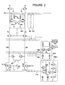
- FIG 2 there is shown a circuit diagram of a first embodiment of the semiconductor memory circuit in accordance with the present invention.
- Figures 3A and 3B show a voltage change in time in a data bus switching over operation of the semiconductor memory circuit shown in Figure 2.
- elements similar to those shown in Figure 1 are given the same Reference Signs, and explanation thereof will be omitted for simplification of description.
- the semiconductor memory circuit shown in Figure 2 additionally comprises a voltage supply circuit DBL1 including three dummy transistors M9, M10 and M11 having the same power and the same shape as those of the three MOS transistors M0 (M1), M2 (M3) and M4 (M5) which determine the data bus potential at the selection time.
- These dummy transistors M9, M10 and M11 are connected in series for generating a reference voltage V DBO which is the same as the data bus potential of the selection time.
- This reference voltage V DBO is connected to a base of a bipolar transistor Q4 which constitutes an emitter follower.
- a voltage supply voltage V CC is connected to an emitter of the bipolar transistor Q4 through a resistor R1 and two diodes D1 and D2 in a forward direction, so that a potential higher than an emitter potential of the bipolar transistor Q4 by 2V f (where V f is a forward direction voltage in a PN junction of each diode) is applied to a base of a bipolar transistor Q5 which constitutes an output emitter follower.
- V DB generated by the voltage supply circuit DBL1 substantially becomes equal to V DB0 and V DB1 .
- a voltage supply circuit current required for clamping the non-selection time data bus potential to a clamp level given by the output voltage V DB generated by the voltage supply circuit DBL1 is only a current of the voltage supply circuit DBL1 itself, and therefore, is on the order of about 1 mA to 2 mA. This remarkably small in comparison with about several tens milliamperes required in the case of increasing the standby current for each data bus line in the conventional semiconductor memory circuit.
- the output voltage V DB generated by the voltage supply circuit DBL1 is connected to the data bus lines DB0 and DB1 through PMOS transistors M7 and M8, respectively.
- the selection signal Y2 for the data bus is applied directly to gates of the PMOS transistors M7 and M8. Therefore, at the non-selection time, namely when the data bus driving NMOS transistors M4 and M5 are off, the PMOS transistors M7 and M8 are on without exception, so that the data bus lines DB0 and DB1 are clamped to the output voltage V DB generated by the voltage supply circuit DBL1.
- the selection signals Y1 and Y2 are turned off so that the MOS transistors M2, M3, M4 and M5 are turned off. In fact, however, the off-timing of the digit line selection signal Y1 and the off-timing of the data bus line selection signal Y2 are liable to deviate from each other.
- the data bus potential rises toward a potential Va determined by dividing a voltage difference V CC - V DB by a conductivity ratio of the transistors M0 (M1), M2 (M3), and M7 (M8).
- the voltage Va is -1 V to -1.5 V.
- the voltage difference V CC - V DB is divided by a conductivity ratio of the transistors M0 (M1), M2 (M3), and M22 (M23).
- the current drive power of the transistors M22 (M23) is small, the voltage Va rises to almost V CC .
- the selection signal Y2 When the selection signal Y2 is actually turned off, the potential of the data bus lines DB0 and DB1 starts to change toward the non-selection time voltage.
- the transistors M7 (M8) of the shown embodiment and the transistors M22 (M23) of the conventional circuit are greatly different in discharge capability, the shown embodiment and the conventional circuit have greatly different time constants.
- the shown embodiment needs only a time on the order of several nanoseconds until the potential of the data bus lines DB0 and DB1 is actually brought to the output voltage V DB generated by the voltage supply circuit DBL1, but the conventional circuit requires a time of 30-ns to 50-ns.
- the drop speed of the data bus line potential is slightly slowed by the permanent-on pull-up transistors M20 and M21.
- the current driving power of the permanent-on pull-up transistors M20 and M21 is small, a restoring time of 40-ns to 60-ns is required after the selection signal Y2 is turned off until the data bus line potential is brought to the set or clamp level V DB .
- the data bus line is brought into the selection condition when the non-selection time potential of the data bus line is not substantially the same as the selection time potential of the data bus line, an access is delayed by a time required until the set voltage of the selection time is restored and the potential of the data bus line is brought into a range allowing a normal operation of the sense amplifier. For example, if the data bus line is about -0.9-V or more, the transistors Q0 and Q1 of the sense amplifier are brought int a saturated condition since the read bus lines RB0 and RB1 are about - 1.5 V.
- the source-drain voltage of the MOS transistor M6 which functions as the current source for the sense amplifier SA becomes about 0.8-V or less.
- the current of the sense amplifier is decreased, and therefore, a delay occurs in a sense operation of the sense amplifier.
- FIG 4 there is shown a second embodiment of the semiconductor memory circuit.
- elements similar to those shown in Figure 2 are given the same Reference Signs, and explanation thereof will be omitted for simplification of description.
- a second switch circuit for a multiplexer operation is located between the data bus lines DB0 and DB1 and the sense amplifier composed of the transistors Q0, Q2 and M6.
- This second switching circuit includes bipolar transistors Q10 to Q13 having commonly connected emitters and bipolar transistors Q20 to Q23 having commonly connected emitters. Bases of the bipolar transistors Q10 to Q13 and Q20 to Q23 are connected to corresponding first data bus lines, as shown in Figure 4.
- the commonly connected emitters of the bipolar transistors Q10 to Q13 and the commonly connected emitters of the bipolar transistors Q20 to Q23 form a pair of second data bus lines SB0 and SB1, which are connected to the bases of the bipolar transistors Q0 and Q1 of the sense amplifier SA.
- the bipolar transistors for the second data bus lines SB0 and SB1 and the bipolar transistors of the sense amplifier SA both are of an emitter coupled type, and therefore, the second data bus lines SB0 and SB1 and the sense amplifier SA are selected by turning on the MOS transistor M8 and MOS transistors M24 and M25 (functioning as a current source), by means of a third selection signal Y3.
- the second switch circuit is formed of a wired OR circuit composed of bipolar transistors having a high driving force, a data transmission time in the second switching circuit is as short as about 0.05-ns to 0.2 ns. For this and other reasons, the access speed can be greatly improved by about 2-ns or more.
- the multiplexing operation of the second switch circuit is realized by a potential difference in the first data bus lines. Therefore, it is required to ensure that a potential of the non-selection side is sufficiently lower than the set potential of the selection side (by for example about 400-mV or less, namely, an operating margin of 300-mV and a data bus amplitude of 100-mV or less).
- a constant voltage circuit DBL2 for generating a common data bus non-selection time potential V DB includes a series-connected dummy transistors M9, M10 and M11 for generating the reference potential V DB0 equivalent to the selection time data bus line potential, and a bipolar transistor Q7 having a base connected to receive the reference potential V DB0 and forming an emitter follower, so that an emitter of the bipolar transistor Q7 gives the set or clamp voltage V DB which is lower than the data bus line potential of the selection time by about 0.8 V. Therefore, this 0.8-V determines the potential difference between the selected first data bus lines and the non-selected first data bus line, independently upon the variations in characteristics attributable to a manufacturing process. This value of 0.8-V is sufficient as the base potential difference in the second switch circuit.
- the deviation in the off-timing between the selection signals Y1 and Y2 in the conventional semiconductor memory circuit causes a large delay in the reading time, since several tens nanoseconds are required to restore the potential of the non-selected data bus line to the appropriate level.
- the change of the selected and non-selected first data bus lines to the respective appropriate levels are rapidly completed within a range of about 1 -ns to 2 ns.
- the data bus can be selected without substantially delaying the information read out of a selected memory cell. Namely, a stable and high speed access can be realized.
- FIG. 5 there is shown a circuit diagram of a third embodiment of the semiconductor memory circuit in accordance with the present invention.
- Figure 6 shows voltage change in time of various points in the case of a writing operation of the third embodiment shown in Figure 5
- the third embodiment includes a writing circuit in addition to the first embodiment.
- the third embodiment includes a pair of MOS transistors M30 and M31 having common connected bases receiving the digit line selection signal Y1.
- the MOS transistors M30 and M31 are connected between the corresponding digit lines D0 and D1 and corresponding write data lines WB0 and WB1, respectively. Either of the write data lines WB0 and WB1 is brought to a lowest potential in accordance with data to be written. Here, assume that the write data line WB1 is brought to the lowest potential.
- bases of the PMOS load transistors M0 and M1 are connected in common to receive a write signal WA.
- the PMOS load transistors M0 and M1 for the digit lines D0 and D1 are turned off in response to the write signal WA
- V T is a threshold of the transistor M31
- transistor M31 is turned on, and therefore, the potential on the digit line D1 drops following the drop of the potential V WB1 on the write data line WB1.
- the load transistor M1 since the load transistor M1 is off, there is no transistor serving to pull up the digit line D1 to the high level voltage supply voltage V CC . Therefore, the potential on the digit line D1 smoothly drops to the lowest potential with no pass-through current flowing from the high level voltage supply voltage V CC to the write data line WB1. With this, data is written into the memory cell.
- the MOS transistor M1 In a recovery operation after the writing, the MOS transistor M1 is turned on at the same time as the write data line WB1 is brought to a high level. Therefore, a charge current flows into the digit line D1 through the MOS transistors M1 and M31. After the MOS transistors M31 is turned off, the charge current is supplied through only the MOS transistor M1, so that the digit line D1 rises to the selection potential at the time of reading. In order to realize a high speed writing and a high speed recovery, it is necessary to quickly raise and drop the digit line potential. In ordinary cases, however, one digit line is connected with a few hundreds memory cells, and therefore, it can be said that several ten picofarads of capacitance is added to each one digit line. Therefore, it has become difficult to obtain a sufficient speed by only the transistors M31 and M1.
- the data bus selection signal is not changed in the writing operation.
- the data bus selection signal Y2 selecting the data bus connected to the memory cell to be written is turned off with some delay time t d1 after the write signals WA and WB are activated, so that all the data buses are brought into the non-selected condition.
- This delay time t d1 of the turn-off of the data bus selection signal for bringing the data bus into the non-selection condition at the time of writing is set to extend until a timing which is later, by 2 ns to 3 ns or more, from a timing where the digit line D1 drops and the data is written to the memory cell.
- the operation for dropping the potential of the digit line is facilitated by the NMOS transistor M5 through the transfer gate MOS transistor M3, and therefore, the writing operation can be speeded up.
- a timing t1 of the turn-on of the data bus selection signal for bringing the data bus into the selection condition at the time of recovery is set at a timing which is later, by 2 ns to 3 ns or more, from a timing where the potential of the digit line D1 rises and becomes substantially equal to the voltage V DB .
- the data bus potential since the data bus potential has been already pulled up to the voltage V DB of - 1 V to -2 V before the recovery operation starts, the data bus operates to pull up the digit line, in the contrary of the conventional operation in which the data bus is pulled up by the digit line. Therefore, the recovery operation, which had required 5 ns to 10 ns in the conventional example, can be shortened to about 2 ns to 4 ns (which is smaller than a half of the conventional recovery time) without additional recovery improving circuit.
Landscapes
- Engineering & Computer Science (AREA)
- Microelectronics & Electronic Packaging (AREA)
- Computer Hardware Design (AREA)
- Static Random-Access Memory (AREA)
- Dram (AREA)
Applications Claiming Priority (2)
| Application Number | Priority Date | Filing Date | Title |
|---|---|---|---|
| JP2078112A JP2550743B2 (ja) | 1990-03-27 | 1990-03-27 | 半導体メモリ回路 |
| JP78112/90 | 1990-03-27 |
Publications (3)
| Publication Number | Publication Date |
|---|---|
| EP0449282A2 true EP0449282A2 (fr) | 1991-10-02 |
| EP0449282A3 EP0449282A3 (en) | 1993-06-16 |
| EP0449282B1 EP0449282B1 (fr) | 1996-05-22 |
Family
ID=13652804
Family Applications (1)
| Application Number | Title | Priority Date | Filing Date |
|---|---|---|---|
| EP91104959A Expired - Lifetime EP0449282B1 (fr) | 1990-03-27 | 1991-03-27 | Circuit de mémoire à semi-conducteurs |
Country Status (4)
| Country | Link |
|---|---|
| US (1) | US5199000A (fr) |
| EP (1) | EP0449282B1 (fr) |
| JP (1) | JP2550743B2 (fr) |
| DE (1) | DE69119636T2 (fr) |
Cited By (2)
| Publication number | Priority date | Publication date | Assignee | Title |
|---|---|---|---|---|
| EP0645772A3 (fr) * | 1993-09-29 | 1995-07-19 | Nippon Electric Co | Dispositif de mémoire à semi-conducteurs. |
| EP0717412A3 (fr) * | 1994-12-15 | 1997-05-28 | Oki Electric Ind Co Ltd | Dispositif de mémoire à semi-conducteurs |
Families Citing this family (7)
| Publication number | Priority date | Publication date | Assignee | Title |
|---|---|---|---|---|
| JP2817490B2 (ja) * | 1992-01-16 | 1998-10-30 | 日本電気株式会社 | スタティック型半導体メモリ読みだし回路 |
| JP3181759B2 (ja) * | 1993-06-10 | 2001-07-03 | 富士通株式会社 | 半導体記憶装置 |
| FR2725103B1 (fr) * | 1994-09-23 | 1996-12-27 | Alcatel Mobile Comm France | Economie d'energie dans un systeme incluant un radiotelephone portatif connecte a un dispositif peripherique |
| US5907251A (en) * | 1996-11-22 | 1999-05-25 | International Business Machines Corp. | Low voltage swing capacitive bus driver device |
| FR2756409B1 (fr) * | 1996-11-28 | 1999-01-15 | Sgs Thomson Microelectronics | Circuit de lecture pour memoire |
| ITRM20010298A1 (it) * | 2001-05-31 | 2002-12-02 | Micron Technology Inc | Interfaccia di comando di utilizzatore con decodificatore programmabile. |
| US8448587B2 (en) * | 2010-01-26 | 2013-05-28 | Cnh Canada, Ltd. | Row unit bounce monitoring system |
Family Cites Families (4)
| Publication number | Priority date | Publication date | Assignee | Title |
|---|---|---|---|---|
| JPS5833635B2 (ja) * | 1979-12-25 | 1983-07-21 | 富士通株式会社 | 半導体記憶装置 |
| JPS613390A (ja) * | 1984-06-15 | 1986-01-09 | Hitachi Ltd | 記憶装置 |
| US4636988A (en) * | 1985-01-07 | 1987-01-13 | Thomson Components-Mostek Corporation | CMOS memory arrangement with reduced data line compacitance |
| JPH0766945B2 (ja) * | 1988-09-06 | 1995-07-19 | 株式会社東芝 | スタティック型メモリ |
-
1990
- 1990-03-27 JP JP2078112A patent/JP2550743B2/ja not_active Expired - Fee Related
-
1991
- 1991-03-27 EP EP91104959A patent/EP0449282B1/fr not_active Expired - Lifetime
- 1991-03-27 US US07/675,836 patent/US5199000A/en not_active Expired - Fee Related
- 1991-03-27 DE DE69119636T patent/DE69119636T2/de not_active Expired - Fee Related
Cited By (4)
| Publication number | Priority date | Publication date | Assignee | Title |
|---|---|---|---|---|
| EP0645772A3 (fr) * | 1993-09-29 | 1995-07-19 | Nippon Electric Co | Dispositif de mémoire à semi-conducteurs. |
| EP0717412A3 (fr) * | 1994-12-15 | 1997-05-28 | Oki Electric Ind Co Ltd | Dispositif de mémoire à semi-conducteurs |
| US5768210A (en) * | 1994-12-15 | 1998-06-16 | Oki Electric Industry Co., Ltd. | Semiconductor memory device |
| US5818787A (en) * | 1994-12-15 | 1998-10-06 | Oki Electric Industry Co., Ltd. | Semiconductor memory device |
Also Published As
| Publication number | Publication date |
|---|---|
| DE69119636T2 (de) | 1997-01-23 |
| US5199000A (en) | 1993-03-30 |
| EP0449282A3 (en) | 1993-06-16 |
| EP0449282B1 (fr) | 1996-05-22 |
| DE69119636D1 (de) | 1996-06-27 |
| JPH03278395A (ja) | 1991-12-10 |
| JP2550743B2 (ja) | 1996-11-06 |
Similar Documents
| Publication | Publication Date | Title |
|---|---|---|
| US5239502A (en) | Bit storage cell | |
| US4161040A (en) | Data-in amplifier for an MISFET memory device having a clamped output except during the write operation | |
| US3983412A (en) | Differential sense amplifier | |
| CN108766493B (zh) | 一种应用于sram的可调节wlud读写辅助电路 | |
| US5963495A (en) | Dynamic sense amplifier with embedded latch | |
| KR100207942B1 (ko) | 개별 비트 라인 회복 회로 | |
| EP0449282B1 (fr) | Circuit de mémoire à semi-conducteurs | |
| US5208773A (en) | Semiconductor memory device having bit lines and word lines different in data reading and data writing | |
| US4417326A (en) | Static semiconductor memory device | |
| EP0050008A2 (fr) | Dispositif semi-conducteur | |
| EP0405105A2 (fr) | Générateur de tension référence pour préchargement de lignes de bit d'une mémoire à transistor | |
| KR100424510B1 (ko) | 반도체기억장치및센스회로방식 | |
| KR890003373B1 (ko) | 씨모오스 반도체 메모리 장치의 입출력 회로 | |
| US4939691A (en) | Static random access memory | |
| GB2159013A (en) | A mos amplifier and semiconductor memory using the same | |
| US5229967A (en) | BICMOS sense circuit for sensing data during a read cycle of a memory | |
| JPH07169290A (ja) | 半導体記憶装置 | |
| KR950005171B1 (ko) | 전류 미러 증폭회로 및 그의 구동 방법 | |
| US4467456A (en) | Memory circuit | |
| US4442509A (en) | Bit line powered translinear memory cell | |
| EP0469834B1 (fr) | Circuit logique BICMOS avec immunité à l'auto-survoltage et méthode adaptée | |
| KR900004633B1 (ko) | 반도체 메모리 장치 | |
| US5475635A (en) | Memory with a combined global data line load and multiplexer | |
| KR0137083B1 (ko) | 반도체 메모리 장치 및 데이타 판독방법 | |
| US5687127A (en) | Sense amplifier of semiconductor memory having an increased reading speed |
Legal Events
| Date | Code | Title | Description |
|---|---|---|---|
| PUAI | Public reference made under article 153(3) epc to a published international application that has entered the european phase |
Free format text: ORIGINAL CODE: 0009012 |
|
| 17P | Request for examination filed |
Effective date: 19910327 |
|
| AK | Designated contracting states |
Kind code of ref document: A2 Designated state(s): DE FR GB |
|
| PUAL | Search report despatched |
Free format text: ORIGINAL CODE: 0009013 |
|
| AK | Designated contracting states |
Kind code of ref document: A3 Designated state(s): DE FR GB |
|
| 17Q | First examination report despatched |
Effective date: 19941221 |
|
| GRAH | Despatch of communication of intention to grant a patent |
Free format text: ORIGINAL CODE: EPIDOS IGRA |
|
| GRAA | (expected) grant |
Free format text: ORIGINAL CODE: 0009210 |
|
| AK | Designated contracting states |
Kind code of ref document: B1 Designated state(s): DE FR GB |
|
| REF | Corresponds to: |
Ref document number: 69119636 Country of ref document: DE Date of ref document: 19960627 |
|
| ET | Fr: translation filed | ||
| PLBE | No opposition filed within time limit |
Free format text: ORIGINAL CODE: 0009261 |
|
| STAA | Information on the status of an ep patent application or granted ep patent |
Free format text: STATUS: NO OPPOSITION FILED WITHIN TIME LIMIT |
|
| 26N | No opposition filed | ||
| REG | Reference to a national code |
Ref country code: GB Ref legal event code: IF02 |
|
| PGFP | Annual fee paid to national office [announced via postgrant information from national office to epo] |
Ref country code: FR Payment date: 20020312 Year of fee payment: 12 |
|
| PGFP | Annual fee paid to national office [announced via postgrant information from national office to epo] |
Ref country code: GB Payment date: 20020327 Year of fee payment: 12 |
|
| PGFP | Annual fee paid to national office [announced via postgrant information from national office to epo] |
Ref country code: DE Payment date: 20020404 Year of fee payment: 12 |
|
| PG25 | Lapsed in a contracting state [announced via postgrant information from national office to epo] |
Ref country code: GB Free format text: LAPSE BECAUSE OF NON-PAYMENT OF DUE FEES Effective date: 20030327 |
|
| PG25 | Lapsed in a contracting state [announced via postgrant information from national office to epo] |
Ref country code: DE Free format text: LAPSE BECAUSE OF NON-PAYMENT OF DUE FEES Effective date: 20031001 |
|
| GBPC | Gb: european patent ceased through non-payment of renewal fee |
Effective date: 20030327 |
|
| PG25 | Lapsed in a contracting state [announced via postgrant information from national office to epo] |
Ref country code: FR Free format text: LAPSE BECAUSE OF NON-PAYMENT OF DUE FEES Effective date: 20031127 |
|
| REG | Reference to a national code |
Ref country code: FR Ref legal event code: ST |