EP0449418A2 - Dispositif à effet de champ à grille isolée avec canal cintré et méthode de fabrication - Google Patents
Dispositif à effet de champ à grille isolée avec canal cintré et méthode de fabrication Download PDFInfo
- Publication number
- EP0449418A2 EP0449418A2 EP91301405A EP91301405A EP0449418A2 EP 0449418 A2 EP0449418 A2 EP 0449418A2 EP 91301405 A EP91301405 A EP 91301405A EP 91301405 A EP91301405 A EP 91301405A EP 0449418 A2 EP0449418 A2 EP 0449418A2
- Authority
- EP
- European Patent Office
- Prior art keywords
- concave
- semiconductor substrate
- main surface
- effect device
- insulated gate
- Prior art date
- Legal status (The legal status is an assumption and is not a legal conclusion. Google has not performed a legal analysis and makes no representation as to the accuracy of the status listed.)
- Withdrawn
Links
- 230000005669 field effect Effects 0.000 title claims abstract description 18
- 238000004519 manufacturing process Methods 0.000 title 1
- 239000000758 substrate Substances 0.000 claims abstract description 43
- 239000004065 semiconductor Substances 0.000 claims abstract description 29
- 239000012535 impurity Substances 0.000 claims abstract description 12
- 230000000694 effects Effects 0.000 claims description 8
- 238000000034 method Methods 0.000 claims description 6
- 238000005530 etching Methods 0.000 claims description 3
- 229910044991 metal oxide Inorganic materials 0.000 claims 1
- 150000004706 metal oxides Chemical class 0.000 claims 1
- 230000015556 catabolic process Effects 0.000 description 5
- XUIMIQQOPSSXEZ-UHFFFAOYSA-N Silicon Chemical compound [Si] XUIMIQQOPSSXEZ-UHFFFAOYSA-N 0.000 description 4
- 229910052710 silicon Inorganic materials 0.000 description 4
- 239000010703 silicon Substances 0.000 description 4
- 230000015572 biosynthetic process Effects 0.000 description 3
- 238000006731 degradation reaction Methods 0.000 description 3
- 238000010586 diagram Methods 0.000 description 3
- 238000009792 diffusion process Methods 0.000 description 3
- 230000007423 decrease Effects 0.000 description 2
- 239000002784 hot electron Substances 0.000 description 2
- 230000010354 integration Effects 0.000 description 2
- 229910052796 boron Inorganic materials 0.000 description 1
- -1 boron ions Chemical class 0.000 description 1
- 238000010884 ion-beam technique Methods 0.000 description 1
- 238000002955 isolation Methods 0.000 description 1
- 230000003647 oxidation Effects 0.000 description 1
- 238000007254 oxidation reaction Methods 0.000 description 1
- 238000001020 plasma etching Methods 0.000 description 1
Images


Classifications
-
- H—ELECTRICITY
- H10—SEMICONDUCTOR DEVICES; ELECTRIC SOLID-STATE DEVICES NOT OTHERWISE PROVIDED FOR
- H10D—INORGANIC ELECTRIC SEMICONDUCTOR DEVICES
- H10D64/00—Electrodes of devices having potential barriers
- H10D64/20—Electrodes characterised by their shapes, relative sizes or dispositions
- H10D64/27—Electrodes not carrying the current to be rectified, amplified, oscillated or switched, e.g. gates
- H10D64/311—Gate electrodes for field-effect devices
- H10D64/411—Gate electrodes for field-effect devices for FETs
- H10D64/511—Gate electrodes for field-effect devices for FETs for IGFETs
Definitions
- the invention relates generally to insulated gate field effect devices. Achievement of a longer effective channel length without increasing the occupying area for insulated gate field effect devices and a method of forming the same will be described.
- FIG. 6 is a sectional view showing a structure of a conventional planar insulated gate field effect device.
- a MOS transistor is indicated in this figure.
- the MOS transistor comprises an n type semiconductor substrate e.g. an n type silicon substrate 6, a p+ source 4 and a p+ drain 5 each formed in the vicinity of the main surface of semiconductor substrate 6 by diffusion, a gate oxide film 22 formed on the main surface of substrate 6, and a conductive layer formed above the main surface of substrate 6 with an insulating film 22 interposed therebetween, i.e. a gate 21.
- a channel region 27 which is indicated by "x" in the figure is formed in the vicinity of the main surface between the source 4 and the drain 5. Since the length of the channel region will be slightly corroded by a diffusion for the formation of the source 4 and the drain 5, an effective channel length Le1 is obtained in practice.
- Figure 7 is a structural sectional view showing the development of a depletion layer in the MOS transistor of Figure 6.
- the source 4 and the drain 5 are grounded to make definite the development of a depletion layer.
- a depletion layer 29 is formed so as to surround the source 4 and the drain 5.
- voltage VG is supplied to the gate 1 causing a depletion layer 20 with a trapezoid configuration to be formed under the gate 1 and between the depletion layers 29.
- the effective channel length Le1 is defined by the longer side of the trapezoid depletion layer 20.
- Substrate voltage Vs is supplied to the substrate 6.
- FIG 8 is a structural sectional diagram of the structure in Figure 7 when seen from the arrow 8.
- a depletion layer 20 having an effective channel width of We1 is formed between local oxidation of silicons (referred to as LOCOS hereinafter) 11 for element isolation.
- Figure 9 is a structural sectional view showing the status when operating voltage is supplied to the MOS transistor of Figure 6.
- voltage VD is supplied to the drain 5
- voltage VG is supplied to the gate 1.
- the source 4 is grounded. It is seen from Figure 9 that the length of channel region 13 retracts from the drain 5 when the operating voltages VD and VG are supplied. In other words, between one end of the channel region 13 and the drain 5, there is a region of a length Lg1 without a channel being formed therein. This means that field concentration will occur in the vicinity of the main surface of the depletion layer 20 near the drain 5.
- This field concentration will cause the following several problems.
- breakdown voltage will occur in the vicinity of the drain due to its field concentration resulting in current to flow into the substrate 6. This means that a greater voltage cannot be supplied to the gate 1 and the drain 5.
- electrons (hot electrons) accelerated by field concentration will flow into the gate oxide film 22 to cause degradation in withstand voltage of the gate oxide film 22.
- the depletion layer 20 has a trapezoid configuration as shown in Figure 9 (this phenomenon is called "fringe effect")
- this phenomenon is called "fringe effect”
- the current is not increased in proportion to the length of the gate.
- the current flowing between the drain and the source increases in proportion to the length of the gate in an insulated gate field effect device.
- the above mentioned fringe effect will hinder the proportional increase of the current. That is to say, as the channel length shortens, threshold voltage Vt decreases. Therefore, subthreshold current will flow to the source 4 from drain 5 when the transistor should be turned off.
- An insulated gate field effect device in accordance with the present invention comprises: a first conductivity type semiconductor substrate having a main surface, said semiconductor substrate having a concave with a curved surface formed on said main surface, an insulating film formed on the main surface including said concave, first and second impurity regions of a second conductivity type formed in the vicinity of said main surface of said semiconductor substrate, and at one side and the other side of said concave, respectively, said first conductivity type region of said semiconductor substrate between said first and second impurity regions having a channel region formed along said concave, and a conductive layer formed above said channel region with said insulating film interposed therebetween.
- the present invention also provides a method of forming an insulated gate filed effect device on a first conductivity type semiconductor substrate having a main surface, comprising the steps of: forming a concave having a curved surface at the main surface of said semiconductor substrate, forming a first insulating film above the main surface including said concave, forming a conductive layer above said concave having been formed in said semiconductor substrate, with said first insulating film interposed therebetween, and forming first and second impurity regions of a second conductivity type at one side and the other side of said concave, respectively, in the vicinity of the main surface of said semiconductor substrate.
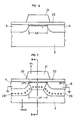
- Figure 1 is a sectional view of the structure of a MOS transistor showing an embodiment of the invention.
- Figure 2 is a structural sectional view showing the development of a depletion layer in the MOS transistor of Figure 1.
- Figure 3 is a sectional structure view of the structure in Figure 2 when seen from a different direction.
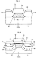
- Figure 4 is a structural sectional view of the state when operating voltages are supplied to the MOS transistor of Figure 1.
- FIGS 5A-5E are processing diagrams showing the formation of the MOS transistor of Figure 1.
- Figure 6 already referred to, is a sectional view showing the structure of a conventional MOS transistor.
- Figure 7 is a structural sectional view showing the development of a depletion layer in the MOS transistor of Figure 6.
- Figure 8 already referred to, is a structural sectional view of the structure in Figure 7 when seen from a different direction.
- Figure 9 is a structural sectional view showing the state when operating voltages are supplied to the MOS transistor of Figure 6.
- 1 is the gate
- 2 is the gate oxide film
- 4 is the source
- 5 is the drain
- 6 is the semiconductor substrate
- 7 is the channel region
- 9 and 10 are the depletion layer
- Le1 and Le2 are the effective channel lengths.
- FIG. 1 is a sectional view of a structure of an insulated gate field effect device showing an embodiment of the invention.
- a MOS transistor is indicated by way of an example.
- the MOS transistor comprises a semiconductor substrate having a concave which is formed as a smooth curve, i.e. a silicon substrate 6, a source 4 and a drain 5 formed on one side and the other side of the concave by diffusion respectively, a gate oxide film 2 formed on the main surface of the substrate 6 including the concave, and a conductive layer formed on the concave, i.e. a gate 1.
- a channel region 7 is formed along the concave between the source 4 and the drain 5 to obtain an effective channel length Le2 that is longer than the effective channel length Le1 shown in Figure 6.
- Figure 2 is a structural sectional view showing the development of a depletion layer in the MOS transistor of Figure 1.
- a source 4 and a drain 5 is provided to facilitate the development of the depletion layer.
- a depletion layer 9 is formed below the source 4 and the drain 5.
- a depletion layer 10 is formed along the concave between the source 4 and the drain 5. When gate voltage VG is supplied, a channel region is formed in the depletion layer 10 along the concave.
- Figure 3 is a structural sectional view of the structure in Figure 2 when seen from the direction of the arrow 3.
- a depletion layer 10 is formed between LOCOS 11 along the concave when gate voltage VI is supplied.
- a channel region 12 having the effective channel width We2 is formed along the concave in the depletion layer 10.
- Figure 4 is a structural sectional view showing the status when operating voltages are supplied to the MOS transistor of Figure 1.
- the MOS transistor of Figure 4 has the same operating voltages shown in Figure 9, that is, has gate voltage VG and drain voltage VD supplied.
- Figure 4 it can be seen that the two MOS transistors have the same occupying area, except that the distance Lg2 between the end of channel region 12 and the drain 5 is longer than the distance Lg1 indicated in Figure 9. That is to say, since the effective channel length Le2 shown in Figure 1 is longer than the effective channel length Le1 shown in Figure 6, the field concentration in the vicinity of the drain is reduced as compared with that of the MOS transistor in Figure 6.
- a strip depletion layer 10 is formed along the concave as shown in Figures 2 and 4, resulting in a current flow which is proportional to the gate length.
- a depletion layer 10 having a trapezoid configuration as shown in Figures 7 and 9 due to fringe effect is formed.
- a strip depletion layer 10 as shown in Figures 2 and 4 is obtained. Consequently, the effect of a short or a long effective channel length is reduced.
- the variation of threshold voltage Vt caused by the variation of the supplied gate voltage can be prevented.
- the generation of the sub threshold current may also be avoided.
- FIGS 5A-5E are diagrams showing the process of forming the MOS transistor of Figure 1.
- an oxide film 2 is formed on a silicon substrate 6, followed by the formation of a patterned resist 21 on the oxide film 2.
- an isotropic etching such as plasma etching or focal ion beam (hereinafter referred to as EB) from above is performed to form a concave on the substrate 6.
- EB focal ion beam
- an oxide film 2 is formed on the substrate 6 including the concave portion, and a conductive layer 1 for constituting a gate is formed at the concave portion of the oxide film 2.
- the depth of the concave formed in the vicinity of the main surface of the substrate 6 is preferably set to the same value of the depth of the source 4 and the drain 5.
- the effect of the embodiment of this invention is most significant when the depth of the concave is set to a value which ranges between the depth of the source 4 and the drain 5 and its twofold. That is to say, when the depth of the drain is 0.5-0.6 ⁇ m, the depth of the concave is set to a maximum of approximately 1.0 ⁇ m.
- the effective channel length will be designed to lie within the range of 0.5 to 1.0 ⁇ m, resulting in the achievement of a 0.7 to 1.4 ⁇ m effective channel length in practice.
- the configuration of the concave should preferably be smooth towards the direction of the drain 5 from the source 4. In other words, it is preferable to form a concave which is comprised of a curved surface. This is because if a concave which does not have a smooth configuration is formed, field concentration will occur at that portion.
- a channel region is formed along a concave between first and second impurity regions to obtain an insulated gate field effect device having a longer effective channel length without increasing the occupying area.
Landscapes
- Insulated Gate Type Field-Effect Transistor (AREA)
Applications Claiming Priority (2)
| Application Number | Priority Date | Filing Date | Title |
|---|---|---|---|
| JP47100/90 | 1990-02-26 | ||
| JP2047100A JPH03254156A (ja) | 1990-02-26 | 1990-02-26 | 絶縁ゲート電界効果素子およびその形成方法 |
Publications (2)
| Publication Number | Publication Date |
|---|---|
| EP0449418A2 true EP0449418A2 (fr) | 1991-10-02 |
| EP0449418A3 EP0449418A3 (en) | 1992-01-02 |
Family
ID=12765760
Family Applications (1)
| Application Number | Title | Priority Date | Filing Date |
|---|---|---|---|
| EP19910301405 Withdrawn EP0449418A3 (en) | 1990-02-26 | 1991-02-21 | Insulated gate field effect device with a curved channel and method of fabrication |
Country Status (2)
| Country | Link |
|---|---|
| EP (1) | EP0449418A3 (fr) |
| JP (1) | JPH03254156A (fr) |
Cited By (1)
| Publication number | Priority date | Publication date | Assignee | Title |
|---|---|---|---|---|
| WO2003009391A1 (fr) * | 2001-07-10 | 2003-01-30 | Sony Corporation | Composant a semi-conducteur tranchee-grille et son procede de fabrication |
-
1990
- 1990-02-26 JP JP2047100A patent/JPH03254156A/ja active Pending
-
1991
- 1991-02-21 EP EP19910301405 patent/EP0449418A3/en not_active Withdrawn
Cited By (1)
| Publication number | Priority date | Publication date | Assignee | Title |
|---|---|---|---|---|
| WO2003009391A1 (fr) * | 2001-07-10 | 2003-01-30 | Sony Corporation | Composant a semi-conducteur tranchee-grille et son procede de fabrication |
Also Published As
| Publication number | Publication date |
|---|---|
| JPH03254156A (ja) | 1991-11-13 |
| EP0449418A3 (en) | 1992-01-02 |
Similar Documents
| Publication | Publication Date | Title |
|---|---|---|
| US5510279A (en) | Method of fabricating an asymmetric lightly doped drain transistor device | |
| JP3221766B2 (ja) | 電界効果トランジスタの製造方法 | |
| JP3049492B2 (ja) | Mosfet及びその製造方法 | |
| US6951792B1 (en) | Dual-oxide transistors for the improvement of reliability and off-state leakage | |
| US4933730A (en) | Semiconductor device having a high breakdown voltage characteristic | |
| US6300207B1 (en) | Depleted sidewall-poly LDD transistor | |
| US6077736A (en) | Method of fabricating a semiconductor device | |
| US5212542A (en) | Semiconductor device having at least two field effect transistors and method of manufacturing the same | |
| US3631312A (en) | High-voltage mos transistor method and apparatus | |
| KR100276744B1 (ko) | Ldd구조를 갖는 반도체 장치와 그 제조방법 | |
| JP3057436B2 (ja) | 半導体デバイス及びその製造方法 | |
| US5623154A (en) | Semiconductor device having triple diffusion | |
| US5248893A (en) | Insulated gate field effect device with a smoothly curved depletion boundary in the vicinity of the channel-free zone | |
| JP2961525B2 (ja) | 半導体装置及びその製造方法 | |
| US6057582A (en) | Semiconductor device with gate electrode having end portions to reduce hot carrier effects | |
| US6597038B1 (en) | MOS transistor with double drain structure for suppressing short channel effect | |
| JP3008154B2 (ja) | 半導体装置の製造方法 | |
| JP3194162B2 (ja) | Mos fet製造方法 | |
| JPH07263693A (ja) | Fetの製造方法及び集積構造 | |
| JPH04264776A (ja) | 半導体装置 | |
| JPH10144922A (ja) | 電界効果トランジスタ(fet)および半導体電界効果トランジスタを形成する方法 | |
| EP0449418A2 (fr) | Dispositif à effet de champ à grille isolée avec canal cintré et méthode de fabrication | |
| US6215153B1 (en) | MOSFET and method for fabricating the same | |
| JP2578662B2 (ja) | 半導体装置の製造方法 | |
| KR100947567B1 (ko) | 고전압 소자 및 그 제조 방법 |
Legal Events
| Date | Code | Title | Description |
|---|---|---|---|
| PUAI | Public reference made under article 153(3) epc to a published international application that has entered the european phase |
Free format text: ORIGINAL CODE: 0009012 |
|
| AK | Designated contracting states |
Kind code of ref document: A2 Designated state(s): AT BE CH DE DK ES FR GB GR IT LI LU NL SE |
|
| PUAL | Search report despatched |
Free format text: ORIGINAL CODE: 0009013 |
|
| AK | Designated contracting states |
Kind code of ref document: A3 Designated state(s): AT BE CH DE DK ES FR GB GR IT LI LU NL SE |
|
| 17P | Request for examination filed |
Effective date: 19920407 |
|
| 17Q | First examination report despatched |
Effective date: 19940317 |
|
| STAA | Information on the status of an ep patent application or granted ep patent |
Free format text: STATUS: THE APPLICATION IS DEEMED TO BE WITHDRAWN |
|
| 18D | Application deemed to be withdrawn |
Effective date: 19970902 |