EP0449496A1 - Procédé pour le montage d'un dispositif semi-conducteur - Google Patents
Procédé pour le montage d'un dispositif semi-conducteur Download PDFInfo
- Publication number
- EP0449496A1 EP0449496A1 EP91302413A EP91302413A EP0449496A1 EP 0449496 A1 EP0449496 A1 EP 0449496A1 EP 91302413 A EP91302413 A EP 91302413A EP 91302413 A EP91302413 A EP 91302413A EP 0449496 A1 EP0449496 A1 EP 0449496A1
- Authority
- EP
- European Patent Office
- Prior art keywords
- semiconductor device
- circuit board
- electrodes
- adhesive
- electrode
- Prior art date
- Legal status (The legal status is an assumption and is not a legal conclusion. Google has not performed a legal analysis and makes no representation as to the accuracy of the status listed.)
- Granted
Links
Images

Classifications
-
- H—ELECTRICITY
- H10—SEMICONDUCTOR DEVICES; ELECTRIC SOLID-STATE DEVICES NOT OTHERWISE PROVIDED FOR
- H10W—GENERIC PACKAGES, INTERCONNECTIONS, CONNECTORS OR OTHER CONSTRUCTIONAL DETAILS OF DEVICES COVERED BY CLASS H10
- H10W74/00—Encapsulations, e.g. protective coatings
- H10W74/01—Manufacture or treatment
- H10W74/012—Manufacture or treatment of encapsulations on active surfaces of flip-chip devices, e.g. forming underfills
-
- H—ELECTRICITY
- H10—SEMICONDUCTOR DEVICES; ELECTRIC SOLID-STATE DEVICES NOT OTHERWISE PROVIDED FOR
- H10W—GENERIC PACKAGES, INTERCONNECTIONS, CONNECTORS OR OTHER CONSTRUCTIONAL DETAILS OF DEVICES COVERED BY CLASS H10
- H10W74/00—Encapsulations, e.g. protective coatings
- H10W74/10—Encapsulations, e.g. protective coatings characterised by their shape or disposition
- H10W74/15—Encapsulations, e.g. protective coatings characterised by their shape or disposition on active surfaces of flip-chip devices, e.g. underfills
-
- H—ELECTRICITY
- H10—SEMICONDUCTOR DEVICES; ELECTRIC SOLID-STATE DEVICES NOT OTHERWISE PROVIDED FOR
- H10W—GENERIC PACKAGES, INTERCONNECTIONS, CONNECTORS OR OTHER CONSTRUCTIONAL DETAILS OF DEVICES COVERED BY CLASS H10
- H10W72/00—Interconnections or connectors in packages
- H10W72/071—Connecting or disconnecting
- H10W72/072—Connecting or disconnecting of bump connectors
-
- H—ELECTRICITY
- H10—SEMICONDUCTOR DEVICES; ELECTRIC SOLID-STATE DEVICES NOT OTHERWISE PROVIDED FOR
- H10W—GENERIC PACKAGES, INTERCONNECTIONS, CONNECTORS OR OTHER CONSTRUCTIONAL DETAILS OF DEVICES COVERED BY CLASS H10
- H10W72/00—Interconnections or connectors in packages
- H10W72/071—Connecting or disconnecting
- H10W72/073—Connecting or disconnecting of die-attach connectors
- H10W72/07331—Connecting techniques
- H10W72/07337—Connecting techniques using a polymer adhesive, e.g. an adhesive based on silicone or epoxy
- H10W72/07338—Connecting techniques using a polymer adhesive, e.g. an adhesive based on silicone or epoxy hardening the adhesive by curing, e.g. thermosetting
-
- H—ELECTRICITY
- H10—SEMICONDUCTOR DEVICES; ELECTRIC SOLID-STATE DEVICES NOT OTHERWISE PROVIDED FOR
- H10W—GENERIC PACKAGES, INTERCONNECTIONS, CONNECTORS OR OTHER CONSTRUCTIONAL DETAILS OF DEVICES COVERED BY CLASS H10
- H10W72/00—Interconnections or connectors in packages
- H10W72/20—Bump connectors, e.g. solder bumps or copper pillars; Dummy bumps; Thermal bumps
- H10W72/241—Dispositions, e.g. layouts
-
- H—ELECTRICITY
- H10—SEMICONDUCTOR DEVICES; ELECTRIC SOLID-STATE DEVICES NOT OTHERWISE PROVIDED FOR
- H10W—GENERIC PACKAGES, INTERCONNECTIONS, CONNECTORS OR OTHER CONSTRUCTIONAL DETAILS OF DEVICES COVERED BY CLASS H10
- H10W72/00—Interconnections or connectors in packages
- H10W72/30—Die-attach connectors
- H10W72/321—Structures or relative sizes of die-attach connectors
-
- H—ELECTRICITY
- H10—SEMICONDUCTOR DEVICES; ELECTRIC SOLID-STATE DEVICES NOT OTHERWISE PROVIDED FOR
- H10W—GENERIC PACKAGES, INTERCONNECTIONS, CONNECTORS OR OTHER CONSTRUCTIONAL DETAILS OF DEVICES COVERED BY CLASS H10
- H10W72/00—Interconnections or connectors in packages
- H10W72/30—Die-attach connectors
- H10W72/351—Materials of die-attach connectors
- H10W72/353—Materials of die-attach connectors not comprising solid metals or solid metalloids, e.g. ceramics
- H10W72/354—Materials of die-attach connectors not comprising solid metals or solid metalloids, e.g. ceramics comprising polymers
-
- H—ELECTRICITY
- H10—SEMICONDUCTOR DEVICES; ELECTRIC SOLID-STATE DEVICES NOT OTHERWISE PROVIDED FOR
- H10W—GENERIC PACKAGES, INTERCONNECTIONS, CONNECTORS OR OTHER CONSTRUCTIONAL DETAILS OF DEVICES COVERED BY CLASS H10
- H10W72/00—Interconnections or connectors in packages
- H10W72/851—Dispositions of multiple connectors or interconnections
- H10W72/853—On the same surface
- H10W72/856—Bump connectors and die-attach connectors
-
- H—ELECTRICITY
- H10—SEMICONDUCTOR DEVICES; ELECTRIC SOLID-STATE DEVICES NOT OTHERWISE PROVIDED FOR
- H10W—GENERIC PACKAGES, INTERCONNECTIONS, CONNECTORS OR OTHER CONSTRUCTIONAL DETAILS OF DEVICES COVERED BY CLASS H10
- H10W90/00—Package configurations
- H10W90/701—Package configurations characterised by the relative positions of pads or connectors relative to package parts
- H10W90/721—Package configurations characterised by the relative positions of pads or connectors relative to package parts of bump connectors
- H10W90/724—Package configurations characterised by the relative positions of pads or connectors relative to package parts of bump connectors between a chip and a stacked insulating package substrate, interposer or RDL
-
- H—ELECTRICITY
- H10—SEMICONDUCTOR DEVICES; ELECTRIC SOLID-STATE DEVICES NOT OTHERWISE PROVIDED FOR
- H10W—GENERIC PACKAGES, INTERCONNECTIONS, CONNECTORS OR OTHER CONSTRUCTIONAL DETAILS OF DEVICES COVERED BY CLASS H10
- H10W90/00—Package configurations
- H10W90/701—Package configurations characterised by the relative positions of pads or connectors relative to package parts
- H10W90/731—Package configurations characterised by the relative positions of pads or connectors relative to package parts of die-attach connectors
- H10W90/734—Package configurations characterised by the relative positions of pads or connectors relative to package parts of die-attach connectors between a chip and a stacked insulating package substrate, interposer or RDL
-
- H—ELECTRICITY
- H10—SEMICONDUCTOR DEVICES; ELECTRIC SOLID-STATE DEVICES NOT OTHERWISE PROVIDED FOR
- H10W—GENERIC PACKAGES, INTERCONNECTIONS, CONNECTORS OR OTHER CONSTRUCTIONAL DETAILS OF DEVICES COVERED BY CLASS H10
- H10W99/00—Subject matter not provided for in other groups of this subclass
Definitions
- the present invention relates to a method for mounting a semiconductor device wherein the semiconductor device is mounted on a circuit board by means of an adhesive.
- an electrode of the semiconductor device and that of a circuit board are pressurized and connected in a so-called face-down state where they are opposed to each other and then fixed by means of a light setting adhesive, a heating step is not needed. Consequently, the semiconductor device and circuit board are not thermally damaged.
- the electrodes are connected to each other with pressure. Accordingly, an electrode material is not limited to a material which can be bonded by metals, i.e., can be soldered. In addition, steps can be carried out simply and quickly.
- the present invention provides a method for mounting a semiconductor device wherein a semiconductor device on which connection electrodes are formed is connected to a circuit board on which electrodes are formed in positions corresponding to the connection electrodes of the semiconductor device, the method comprising steps of applying an adhesive on a connection face of the semiconductor device to the circuit board or that of the circuit board to the semiconductor device, aligning the electrodes in positions corresponding to each other with the semiconductor device opposed to the circuit board, partially curing the adhesive in portions other than the electrodes, electrically evaluating the connection of the semiconductor device to the circuit board, and curing the uncured adhesive.
- the circuit board may be translucent and the adhesive may have light setting properties.
- the electrode of the semiconductor device and that of the circuit board may electrically be connected to each other with pressure through conductive particles.
- the electrode of the semiconductor device may be a bump electrode and may electrically be connected to the electrode of the circuit board with pressure.
- the method for mounting a semiconductor device further comprises a step of pressurizing the semiconductor device onto the circuit board between the steps of aligning and partially curing the adhesive.
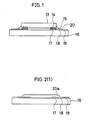
- Fig. 1 is a section view showing a structure in which a semiconductor device 13 is mounted on a circuit board 16.
- the semiconductor device 13 is made of a material such as silicon or gallium arsenic.
- the semiconductor device 13 has an integrated circuit formed on one of surfaces thereof.
- the integrated circuit includes a lot of transistors, diodes and the like (not shown).
- An electrode 14 to be connected to a connection electrode 17 on the circuit board 16 is formed on the periphery of the integrated circuit.
- Conductive particles 15 as connection members are disposed on the electrode 14 (see Japanese Unexamined Patent Publication No. 2-23623 for further details of the conductive particles 15).
- the circuit board 16 is formed of a translucent material such as glass.
- the electrode 17 having the size corresponding to the electrode 14 is formed in a position corresponding to the electrode 14 on one of surfaces of the circuit board 16.
- the electrode 17 is connected to an electrode 19 for an electric test through a wire 18.
- the electrode 19 for an electric test is formed on the circuit board 16.
- the electrode 14 of the semiconductor device 13 is electrically connected to the electrode 17 of the circuit board 16 with pressure through the conductive particles 15. In this state, the semiconductor device 13 is fixed onto the circuit board 16 by means of a light setting adhesive 20 (for example, No. 350 manufactured by Nippon Lock Tight Kabushiki Kaisha).
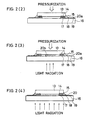
- an uncured light setting adhesive layer 20a is formed in a region where the semiconductor device 13 is to be mounted on the circuit board 16 by printing, transfer or dispenser dropping.
- the semiconductor device 13 is disposed and pressurized on the circuit board 16 in such a manner that the electrodes 14 and 17 are opposed to each other.
- a light setting adhesive layer 20b is cured by irradiating light having a cure wavelength of the light setting adhesive.
- the light setting adhesive layer 20b is formed in a region where the electrode 14 of the semiconductor device 13 does not exist between the semiconductor device 13 and the circuit board 16, i.e., a central region. Consequently, the electrode 14 of the semiconductor device 13 is electrically connected to the electrode 17 of the circuit board 16 after pressurization. In addition, the light setting adhesive is kept uncured in an electrode portion.
- the light having the cure wavelength of the light setting adhesive is irradiated on an entire region of the light setting adhesive layer 20 through the circuit board 16 so that the uncured light setting adhesive is cured as shown in Fig. 2 (4).
- mounting is completed.
- the light passing through the back of the circuit board 16 is reflected and scattered by the semiconductor device 13 so that the light setting adhesive layer 20 of the electrode 17 is cured. Consequently, it is not required to always use a transparent electrode for the electrode 17.
- a heating temperature depends on physical properties of the light setting adhesive.
- the heating temperature is 100 to 200°C.
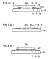
- the cured matter 20b of the light setting adhesive exists in a central portion of a semiconductor device mounting region, in which the connection electrode 17 is not provided, on the circuit board 16.
- the light setting adhesive 20a in a peripheral portion including the electrode 17 is kept uncured.
- the light setting adhesive is further supplied onto the semiconductor device mounting region of the circuit board 16 by a dispenser dropping method or the like. Then, another semiconductor device 13a is mounted according to the method for mounting a semiconductor device mentioned above (see Fig. 3 (3)).
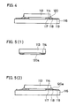
- Fig. 4 is a section view showing a structure in which a semiconductor device 113 is mounted on a circuit board 116.
- the semiconductor device 113 is made of a material such as silicon or gallium arsenic.
- the semiconductor device 113 has an integrated circuit formed on one of surfaces thereof.
- the integrated circuit includes a lot of transistors, diodes and the like (not shown).
- a bump electrode 114 to be connected to a connection electrode 117 on the circuit board 116 is formed on the periphery of the integrated circuit.
- the circuit board 116 is formed of a translucent material such as glass.
- the electrode 117 having the size corresponding to the bump electrode 114 is formed in a position corresponding to the bump electrode 114 on one of surfaces of the circuit board 116.
- the electrode 117 is connected to an electrode 119 for an electric test through a wire 118.
- the electrode 119 for an electric test is formed on the circuit board 116.
- the bump electrode 114 of the semiconductor device 113 is electrically connected to the electrode 117 of the circuit board 116 with pressure. In this state, the semiconductor device 113 is fixed onto the circuit board 116 by means of a light setting adhesive 120.
- an uncured light setting adhesive layer 120a is formed on the side, on which the bump electrode 114 of the semiconductor device 113 is formed, by printing, transfer or dispenser dropping.
- the semiconductor device 113 is aligned and disposed on the circuit board 116 in such a manner that the bump electrode 114 is opposed to the electrode 117.
- a light setting adhesive layer 120b is cured by irradiating light having a cure wavelength of the light setting adhesive.
- the light setting adhesive layer 120b is formed in a region where the bump electrode 114 of the semiconductor device 113 does not exist between the semiconductor device 113 and the circuit board 116, i.e., a central region. Consequently, the semiconductor device 113 is temporarily fixed onto the circuit board 116. In such a state, it is not required to always connect the bump electrode 114 of the semiconductor device 113 to the electrode 117 of the circuit board 116 electrically.
- the semiconductor device 113 is pressurized on the circuit board 116 so as to electrically connect the bump electrode 114 of the semiconductor device 113 to the electrode 117 of the circuit board 116.
- an electric test is given to the semiconductor device 113 through the electrode 119 for an electric test formed on the circuit board 116.
- the light having the cure wavelength of the light setting adhesive is irradiated on an entire region of the light setting adhesive layer 120 through the circuit board 116 in a state where the semiconductor device 113 is pressurized on the circuit board 116 as shown in Fig. 5 (4). Consequently, the uncured light setting adhesive is cured. As a result, mounting is completed.
- a connection structure of the electrodes of the semiconductor device is not limited to the above-mentioned embodiments. It is needless to say- that the present invention can be applied to a semiconductor device capable of being mounted with pressure by means of a light setting adhesive.
- the present invention there is cured only a light setting adhesive on a connection face of the semiconductor device to the circuit board in a central region where electrodes do not exist. Then, an electric test is given. Consequently, even if defects in the semiconductor device or in connection of the semiconductor device to the circuit board are found as a result of the electric test so that it is required to exchange the semiconductor device, another semiconductor device can easily be mounted again without removing the light setting adhesive on the circuit board.
Landscapes
- Wire Bonding (AREA)
Applications Claiming Priority (4)
| Application Number | Priority Date | Filing Date | Title |
|---|---|---|---|
| JP7029690 | 1990-03-20 | ||
| JP70296/90 | 1990-03-20 | ||
| JP2274650A JP2547895B2 (ja) | 1990-03-20 | 1990-10-12 | 半導体装置の実装方法 |
| JP274650/90 | 1990-10-12 |
Publications (2)
| Publication Number | Publication Date |
|---|---|
| EP0449496A1 true EP0449496A1 (fr) | 1991-10-02 |
| EP0449496B1 EP0449496B1 (fr) | 1994-07-20 |
Family
ID=26411462
Family Applications (1)
| Application Number | Title | Priority Date | Filing Date |
|---|---|---|---|
| EP91302413A Expired - Lifetime EP0449496B1 (fr) | 1990-03-20 | 1991-03-20 | Procédé pour le montage d'un dispositif semi-conducteur |
Country Status (2)
| Country | Link |
|---|---|
| EP (1) | EP0449496B1 (fr) |
| DE (1) | DE69102919T2 (fr) |
Cited By (3)
| Publication number | Priority date | Publication date | Assignee | Title |
|---|---|---|---|---|
| EP0642157A1 (fr) * | 1993-09-06 | 1995-03-08 | Commissariat A L'energie Atomique | Procédé d'assemblage de composants par collage |
| AP648A (en) * | 1995-01-10 | 1998-05-25 | Smithkline Beecham Farm S P A | Indole derivatives useful in the treatment of osteoporosis. |
| EP0954021A1 (fr) * | 1998-04-30 | 1999-11-03 | SCHLUMBERGER Systèmes | Procédé de réalisation d'un composant électronique et composant électronique |
Citations (3)
| Publication number | Priority date | Publication date | Assignee | Title |
|---|---|---|---|---|
| US4811081A (en) * | 1987-03-23 | 1989-03-07 | Motorola, Inc. | Semiconductor die bonding with conductive adhesive |
| EP0321238A2 (fr) * | 1987-12-17 | 1989-06-21 | Matsushita Electric Industrial Co., Ltd. | Procédé pour la connexion d'une électrode |
| EP0321239A2 (fr) * | 1987-12-17 | 1989-06-21 | Matsushita Electric Industrial Co., Ltd. | Procédé pour la fabrication d'un dispositif semi-conducteur |
-
1991
- 1991-03-20 EP EP91302413A patent/EP0449496B1/fr not_active Expired - Lifetime
- 1991-03-20 DE DE69102919T patent/DE69102919T2/de not_active Expired - Fee Related
Patent Citations (3)
| Publication number | Priority date | Publication date | Assignee | Title |
|---|---|---|---|---|
| US4811081A (en) * | 1987-03-23 | 1989-03-07 | Motorola, Inc. | Semiconductor die bonding with conductive adhesive |
| EP0321238A2 (fr) * | 1987-12-17 | 1989-06-21 | Matsushita Electric Industrial Co., Ltd. | Procédé pour la connexion d'une électrode |
| EP0321239A2 (fr) * | 1987-12-17 | 1989-06-21 | Matsushita Electric Industrial Co., Ltd. | Procédé pour la fabrication d'un dispositif semi-conducteur |
Non-Patent Citations (2)
| Title |
|---|
| PATENT ABSTRACTS OF JAPAN vol. 013, no. 268 (E-773) 15 June 1989, & JP-A-01 054739 (MATSUSHITA ELECTRIC INDUSTRIAL CO. LTD.) 02 March 1989, * |
| PATENT ABSTRACTS OF JAPAN vol. 014, no. 268 (E-939) 11 June 1990, & JP-A-02 084747 (SEIKO EPSON CORP.) 26 March 1990, * |
Cited By (6)
| Publication number | Priority date | Publication date | Assignee | Title |
|---|---|---|---|---|
| EP0642157A1 (fr) * | 1993-09-06 | 1995-03-08 | Commissariat A L'energie Atomique | Procédé d'assemblage de composants par collage |
| FR2709871A1 (fr) * | 1993-09-06 | 1995-03-17 | Commissariat Energie Atomique | Procédé d'assemblage de composants par hybridation et collage. |
| AP648A (en) * | 1995-01-10 | 1998-05-25 | Smithkline Beecham Farm S P A | Indole derivatives useful in the treatment of osteoporosis. |
| EP0954021A1 (fr) * | 1998-04-30 | 1999-11-03 | SCHLUMBERGER Systèmes | Procédé de réalisation d'un composant électronique et composant électronique |
| FR2778308A1 (fr) * | 1998-04-30 | 1999-11-05 | Schlumberger Systems & Service | Procede de realisation d'un composant electronique et composant electronique |
| US6281048B1 (en) | 1998-04-30 | 2001-08-28 | Schlumberger Systemes | Method of making an electronic component, and an electronic component |
Also Published As
| Publication number | Publication date |
|---|---|
| EP0449496B1 (fr) | 1994-07-20 |
| DE69102919D1 (de) | 1994-08-25 |
| DE69102919T2 (de) | 1994-12-15 |
Similar Documents
| Publication | Publication Date | Title |
|---|---|---|
| US5296063A (en) | Method for mounting a semiconductor device | |
| US6040630A (en) | Integrated circuit package for flip chip with alignment preform feature and method of forming same | |
| US5525545A (en) | Semiconductor chip assemblies and components with pressure contact | |
| KR100244583B1 (ko) | 액정표시장치및그제조방법 | |
| EP0641019A2 (fr) | Cadre de montage flexible imprimé sur un polymère | |
| KR970066683A (ko) | 액정장치, 액정장치의 제조방법 및 전자기기 | |
| KR0179717B1 (ko) | 반도체 패키지의 제조방법과 반도체의 실장방법 및 반도체 실장장치 | |
| JPH06232186A (ja) | 電子部品の接着方法 | |
| JPH05347464A (ja) | 電気回路基板の接続構造および接続方法 | |
| EP0449496B1 (fr) | Procédé pour le montage d'un dispositif semi-conducteur | |
| JPH05102343A (ja) | 半導体装置の実装構造及び半導体装置の実装方法 | |
| JPH07226569A (ja) | 回路基板並びに電極接続体及びその製造方法 | |
| JPH0121620B2 (fr) | ||
| US20030011078A1 (en) | Semiconductor module and producing method therefor | |
| JP2002299809A (ja) | 電子部品の実装方法および実装装置 | |
| JPS62132331A (ja) | 半導体装置の製造方法 | |
| JP3267071B2 (ja) | Tab−セル圧着装置及び圧着方法 | |
| EP0501414A1 (fr) | Méthode de connexion d'électrodes pour dispositif d'affichage | |
| JP2596633B2 (ja) | 半導体素子の実装方法 | |
| JPH05297401A (ja) | 回路基板の接続方法 | |
| JP2706405B2 (ja) | 半導体チップの実装方法 | |
| JPH0541409A (ja) | 接着剤及びそれを用いた実装構造 | |
| JP2827565B2 (ja) | 半導体装置の製造方法 | |
| JP3816144B2 (ja) | 圧着ヘッド及びそれを用いた表示パネルの製造方法 | |
| JPH08102464A (ja) | 突起電極構造とその形成方法及び突起電極を用いた接続構造とその接続方法 |
Legal Events
| Date | Code | Title | Description |
|---|---|---|---|
| PUAI | Public reference made under article 153(3) epc to a published international application that has entered the european phase |
Free format text: ORIGINAL CODE: 0009012 |
|
| 17P | Request for examination filed |
Effective date: 19910411 |
|
| AK | Designated contracting states |
Kind code of ref document: A1 Designated state(s): DE FR GB |
|
| 17Q | First examination report despatched |
Effective date: 19930714 |
|
| GRAA | (expected) grant |
Free format text: ORIGINAL CODE: 0009210 |
|
| AK | Designated contracting states |
Kind code of ref document: B1 Designated state(s): DE FR GB |
|
| PG25 | Lapsed in a contracting state [announced via postgrant information from national office to epo] |
Ref country code: FR Effective date: 19940720 |
|
| REF | Corresponds to: |
Ref document number: 69102919 Country of ref document: DE Date of ref document: 19940825 |
|
| EN | Fr: translation not filed | ||
| PLBE | No opposition filed within time limit |
Free format text: ORIGINAL CODE: 0009261 |
|
| STAA | Information on the status of an ep patent application or granted ep patent |
Free format text: STATUS: NO OPPOSITION FILED WITHIN TIME LIMIT |
|
| 26N | No opposition filed | ||
| PGFP | Annual fee paid to national office [announced via postgrant information from national office to epo] |
Ref country code: DE Payment date: 20010312 Year of fee payment: 11 |
|
| PGFP | Annual fee paid to national office [announced via postgrant information from national office to epo] |
Ref country code: GB Payment date: 20010314 Year of fee payment: 11 |
|
| REG | Reference to a national code |
Ref country code: GB Ref legal event code: IF02 |
|
| PG25 | Lapsed in a contracting state [announced via postgrant information from national office to epo] |
Ref country code: GB Free format text: LAPSE BECAUSE OF NON-PAYMENT OF DUE FEES Effective date: 20020320 |
|
| PG25 | Lapsed in a contracting state [announced via postgrant information from national office to epo] |
Ref country code: DE Free format text: LAPSE BECAUSE OF NON-PAYMENT OF DUE FEES Effective date: 20021001 |
|
| GBPC | Gb: european patent ceased through non-payment of renewal fee |
Effective date: 20020320 |