EP0449640B1 - Method for mounting electrical components. - Google Patents
Method for mounting electrical components. Download PDFInfo
- Publication number
- EP0449640B1 EP0449640B1 EP91302781A EP91302781A EP0449640B1 EP 0449640 B1 EP0449640 B1 EP 0449640B1 EP 91302781 A EP91302781 A EP 91302781A EP 91302781 A EP91302781 A EP 91302781A EP 0449640 B1 EP0449640 B1 EP 0449640B1
- Authority
- EP
- European Patent Office
- Prior art keywords
- electrical components
- metal base
- recesses
- electrical
- circuit board
- Prior art date
- Legal status (The legal status is an assumption and is not a legal conclusion. Google has not performed a legal analysis and makes no representation as to the accuracy of the status listed.)
- Expired - Lifetime
Links
Images


Classifications
-
- H—ELECTRICITY
- H05—ELECTRIC TECHNIQUES NOT OTHERWISE PROVIDED FOR
- H05K—PRINTED CIRCUITS; CASINGS OR CONSTRUCTIONAL DETAILS OF ELECTRIC APPARATUS; MANUFACTURE OF ASSEMBLAGES OF ELECTRICAL COMPONENTS
- H05K1/00—Printed circuits
- H05K1/02—Details
- H05K1/0201—Thermal arrangements, e.g. for cooling, heating or preventing overheating
- H05K1/0203—Cooling of mounted components
-
- H—ELECTRICITY
- H02—GENERATION; CONVERSION OR DISTRIBUTION OF ELECTRIC POWER
- H02M—APPARATUS FOR CONVERSION BETWEEN AC AND AC, BETWEEN AC AND DC, OR BETWEEN DC AND DC, AND FOR USE WITH MAINS OR SIMILAR POWER SUPPLY SYSTEMS; CONVERSION OF DC OR AC INPUT POWER INTO SURGE OUTPUT POWER; CONTROL OR REGULATION THEREOF
- H02M7/00—Conversion of AC power input into DC power output; Conversion of DC power input into AC power output
- H02M7/003—Constructional details, e.g. physical layout, assembly, wiring or busbar connections
-
- H—ELECTRICITY
- H05—ELECTRIC TECHNIQUES NOT OTHERWISE PROVIDED FOR
- H05K—PRINTED CIRCUITS; CASINGS OR CONSTRUCTIONAL DETAILS OF ELECTRIC APPARATUS; MANUFACTURE OF ASSEMBLAGES OF ELECTRICAL COMPONENTS
- H05K7/00—Constructional details common to different types of electric apparatus
- H05K7/20—Modifications to facilitate cooling, ventilating, or heating
- H05K7/2039—Modifications to facilitate cooling, ventilating, or heating characterised by the heat transfer by conduction from the heat generating element to a dissipating body
- H05K7/20436—Inner thermal coupling elements in heat dissipating housings, e.g. protrusions or depressions integrally formed in the housing
-
- H—ELECTRICITY
- H05—ELECTRIC TECHNIQUES NOT OTHERWISE PROVIDED FOR
- H05K—PRINTED CIRCUITS; CASINGS OR CONSTRUCTIONAL DETAILS OF ELECTRIC APPARATUS; MANUFACTURE OF ASSEMBLAGES OF ELECTRICAL COMPONENTS
- H05K7/00—Constructional details common to different types of electric apparatus
- H05K7/20—Modifications to facilitate cooling, ventilating, or heating
- H05K7/2039—Modifications to facilitate cooling, ventilating, or heating characterised by the heat transfer by conduction from the heat generating element to a dissipating body
- H05K7/20436—Inner thermal coupling elements in heat dissipating housings, e.g. protrusions or depressions integrally formed in the housing
- H05K7/20445—Inner thermal coupling elements in heat dissipating housings, e.g. protrusions or depressions integrally formed in the housing the coupling element being an additional piece, e.g. thermal standoff
- H05K7/20463—Filling compound, e.g. potted resin
-
- H—ELECTRICITY
- H10—SEMICONDUCTOR DEVICES; ELECTRIC SOLID-STATE DEVICES NOT OTHERWISE PROVIDED FOR
- H10W—GENERIC PACKAGES, INTERCONNECTIONS, CONNECTORS OR OTHER CONSTRUCTIONAL DETAILS OF DEVICES COVERED BY CLASS H10
- H10W40/00—Arrangements for thermal protection or thermal control
- H10W40/20—Arrangements for cooling
- H10W40/22—Arrangements for cooling characterised by their shape, e.g. having conical or cylindrical projections
-
- H—ELECTRICITY
- H10—SEMICONDUCTOR DEVICES; ELECTRIC SOLID-STATE DEVICES NOT OTHERWISE PROVIDED FOR
- H10W—GENERIC PACKAGES, INTERCONNECTIONS, CONNECTORS OR OTHER CONSTRUCTIONAL DETAILS OF DEVICES COVERED BY CLASS H10
- H10W40/00—Arrangements for thermal protection or thermal control
- H10W40/60—Securing means for detachable heating or cooling arrangements, e.g. clamps
- H10W40/611—Bolts or screws
-
- H—ELECTRICITY
- H10—SEMICONDUCTOR DEVICES; ELECTRIC SOLID-STATE DEVICES NOT OTHERWISE PROVIDED FOR
- H10W—GENERIC PACKAGES, INTERCONNECTIONS, CONNECTORS OR OTHER CONSTRUCTIONAL DETAILS OF DEVICES COVERED BY CLASS H10
- H10W72/00—Interconnections or connectors in packages
-
- H—ELECTRICITY
- H05—ELECTRIC TECHNIQUES NOT OTHERWISE PROVIDED FOR
- H05K—PRINTED CIRCUITS; CASINGS OR CONSTRUCTIONAL DETAILS OF ELECTRIC APPARATUS; MANUFACTURE OF ASSEMBLAGES OF ELECTRICAL COMPONENTS
- H05K2201/00—Indexing scheme relating to printed circuits covered by H05K1/00
- H05K2201/06—Thermal details
- H05K2201/062—Means for thermal insulation, e.g. for protection of parts
-
- H—ELECTRICITY
- H05—ELECTRIC TECHNIQUES NOT OTHERWISE PROVIDED FOR
- H05K—PRINTED CIRCUITS; CASINGS OR CONSTRUCTIONAL DETAILS OF ELECTRIC APPARATUS; MANUFACTURE OF ASSEMBLAGES OF ELECTRICAL COMPONENTS
- H05K2201/00—Indexing scheme relating to printed circuits covered by H05K1/00
- H05K2201/09—Shape and layout
- H05K2201/09209—Shape and layout details of conductors
- H05K2201/09654—Shape and layout details of conductors covering at least two types of conductors provided for in H05K2201/09218 - H05K2201/095
- H05K2201/09745—Recess in conductor, e.g. in pad or in metallic substrate
-
- H—ELECTRICITY
- H05—ELECTRIC TECHNIQUES NOT OTHERWISE PROVIDED FOR
- H05K—PRINTED CIRCUITS; CASINGS OR CONSTRUCTIONAL DETAILS OF ELECTRIC APPARATUS; MANUFACTURE OF ASSEMBLAGES OF ELECTRICAL COMPONENTS
- H05K2201/00—Indexing scheme relating to printed circuits covered by H05K1/00
- H05K2201/10—Details of components or other objects attached to or integrated in a printed circuit board
- H05K2201/10007—Types of components
- H05K2201/10015—Non-printed capacitor
-
- H—ELECTRICITY
- H05—ELECTRIC TECHNIQUES NOT OTHERWISE PROVIDED FOR
- H05K—PRINTED CIRCUITS; CASINGS OR CONSTRUCTIONAL DETAILS OF ELECTRIC APPARATUS; MANUFACTURE OF ASSEMBLAGES OF ELECTRICAL COMPONENTS
- H05K2201/00—Indexing scheme relating to printed circuits covered by H05K1/00
- H05K2201/10—Details of components or other objects attached to or integrated in a printed circuit board
- H05K2201/10227—Other objects, e.g. metallic pieces
- H05K2201/10409—Screws
-
- H—ELECTRICITY
- H05—ELECTRIC TECHNIQUES NOT OTHERWISE PROVIDED FOR
- H05K—PRINTED CIRCUITS; CASINGS OR CONSTRUCTIONAL DETAILS OF ELECTRIC APPARATUS; MANUFACTURE OF ASSEMBLAGES OF ELECTRICAL COMPONENTS
- H05K2201/00—Indexing scheme relating to printed circuits covered by H05K1/00
- H05K2201/10—Details of components or other objects attached to or integrated in a printed circuit board
- H05K2201/10431—Details of mounted components
- H05K2201/1056—Metal over component, i.e. metal plate over component mounted on or embedded in PCB
-
- H—ELECTRICITY
- H05—ELECTRIC TECHNIQUES NOT OTHERWISE PROVIDED FOR
- H05K—PRINTED CIRCUITS; CASINGS OR CONSTRUCTIONAL DETAILS OF ELECTRIC APPARATUS; MANUFACTURE OF ASSEMBLAGES OF ELECTRICAL COMPONENTS
- H05K3/00—Apparatus or processes for manufacturing printed circuits
- H05K3/30—Assembling printed circuits with electric components, e.g. with resistors
- H05K3/32—Assembling printed circuits with electric components, e.g. with resistors electrically connecting electric components or wires to printed circuits
- H05K3/325—Assembling printed circuits with electric components, e.g. with resistors electrically connecting electric components or wires to printed circuits by abutting or pinching; Mechanical auxiliary parts therefor
-
- H—ELECTRICITY
- H10—SEMICONDUCTOR DEVICES; ELECTRIC SOLID-STATE DEVICES NOT OTHERWISE PROVIDED FOR
- H10W—GENERIC PACKAGES, INTERCONNECTIONS, CONNECTORS OR OTHER CONSTRUCTIONAL DETAILS OF DEVICES COVERED BY CLASS H10
- H10W40/00—Arrangements for thermal protection or thermal control
- H10W40/20—Arrangements for cooling
- H10W40/231—Arrangements for cooling characterised by their places of attachment or cooling paths
-
- H—ELECTRICITY
- H10—SEMICONDUCTOR DEVICES; ELECTRIC SOLID-STATE DEVICES NOT OTHERWISE PROVIDED FOR
- H10W—GENERIC PACKAGES, INTERCONNECTIONS, CONNECTORS OR OTHER CONSTRUCTIONAL DETAILS OF DEVICES COVERED BY CLASS H10
- H10W74/00—Encapsulations, e.g. protective coatings
Definitions
- This invention relates to a method of producing an electrical device for mounting electrical components by which method a variety of electrical components can be assembled compactly with enhanced assembling efficiency.
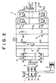
- Fig. 2 is a circuit diagram of an electrical device disclosed, for example, in Japanese laid-open utility model application No. 60-151186.
- Fig. 3 is a top view of the electrical device for mounting electrical components of the circuit of Fig. 2, and Figs. 4 and 5 show the sections along the lines A-A and B-B of Fig. 3, respectively. As shown in Fig.
- the circuit is an inverter circuit for converting the frequency, etc., of a three-phase power, and thus includes: an electromagnetic contactor 1 for turning on and off the power; reactors 2; control transformer 3 for converting the input voltage to a predetermined voltage level; diode bridge rectifier circuit 4 for rectifying the AC current; smoothing capacitor 5 for smoothing the DC current rectified via the diode bridge rectifier circuit 4; discharge transistor 6 for discharging the current charging the capacitors such as smoothing capacitor 5; and transistor inverter circuit 7 for converting the DC current, smoothed via the smoothing capacitor 5, into an AC current of desired frequency.
- Mold resin box 9 accommodates the electromagnetic contactor 1, the reactors 2, the control transformer 3, and the smoothing capacitor 5.
- An electrically insulating substrate 10 is provided with short bars for making large-current-carrying electrical connections among the terminals 14 of the electromagnetic contactor 1, the smoothing capacitor 5, the transistor invertor circuit 7, etc.
- a printed circuit board 11 includes electronic elements for generating control signals.
- the mold resin box 9 is provided with a cover 12 (removed in Figs. 3 and 5).
- the electrical components are fixed via screws on finned aluminum base 8 or within mold resin box 9, in such a manner that the terminals 14 of the electrical components are leveled in their height.
- the electrically insulating substrate 10 is disposed above the electrical components, such that the short bars on the electrically insulating substrate 10 are in contact with the terminals 14 of the electrical components.
- the printed circuit board 11 is positioned above the electrically insulating substrate 10 with a predetermined gap formed therebetween. Screws 13 extending through the printed circuit board 11 and the short bars and the electrically insulating substrate 10 secure the electrically insulating substrate 10 and the printed circuit board 11 such that secure electrical connections among the electrical components are ensured. It is noted that the finned aluminum base 8 carries the electrical components which generate a large amount of heat.
- the above electrical device for mounting electrical components has the following disadvantages.
- the device is in need of two bases, the finned aluminun base 8 and the mold resin box 9. Thus, it is difficult to reduce the overall size of the electrical device for mounting electrical components.
- DE-A-2919058 discloses an electrical device for mounting electrical components, comprising: a base having a plurality of recesses formed on one side thereof for receiving electrical components having terminals projecting therefrom, wherein said recesses have dimensions corresponding to exterior dimensions of the electrical components accommodated therein, such that said terminals of the respective electrical components accommodated in the recesses will project to a predetermined height above the base; and a circuit board carrying a predetermined pattern of electrical conductors thereon, said circuit board being positioned above said one side of the base such that said terminals of the electrical components are in electrical contact with said pattern of electrical conductors carried on said circuit board.
- IBM Technical Disclosure Bulletin Vol. 14 No. 1 June 1971 page 182 discloses an external heat sink for a module fastened to a circuit board.
- the heat sink has a recess accommodating the module and locates the module with its terminals in contact with terminals of the circuit board.
- An object of the present invention is to provide a method of producing an electrical device for mounting a variety of electrical components of different heat-generating capacity, providing a compact assembly, with enhanced assembling efficiency and precision.
- a method of producing an electrical device for mounting electrical components comprises the steps of: forming a metal base having on one side thereof recesses for receiving the electrical components, said recesses having dimensions corresponding to exterior dimensions of the respective electrical components received therein, such that terminals of the respective electrical components accommodated in the recesses will project to a predetermined height above the metal base; fixing board-mounted electrical components on a circuit board carrying a pattern of electrical conductors thereon; pouring predetermined amounts of a high heat conductivity resin and a heat insulating resin into respective recesses of the metal base intended to accommodate components generating large and small amounts of heat respectively; inserting, before the resins are set, electrical components other than said board-mounted electrical components into respective recesses of the metal base; and positioning, before the resins are set, said circuit board above said side of the metal base having the recesses formed therein and inserting the board-mounted electrical components carried on said circuit board into respective recesses of the metal base, terminals of
- An aluminum metal base 20, made via aluminum die casting process, is provided, at the upper side thereof, with a plurality of recesses 20a for receiving and fittingly accommodating the electrical components, and, at the bottom side thereof, with radiating fins 20b for radiating the heat generated by the electrical components.
- the recesses 20a, formed at predetermined positions on the metal base 20, have dimensions corresponding to the respective heights and the shapes of the electrical components accommodated therein, such that the terminals of the electrical components are leveled, i.e., extend above the upper surface of the metal base 20 to substantially the same height.
- the recesses 20a and the radiating fins 20b are formed simultaneously when the metal base 20 is cast by aluminum die casting process.
- a printed circuit board 21 having a predetermined pattern of electrical conductors 21a is disposed above t he metal base 20 to make electrical connections among the electrical components accommodated in the respective recesses 20a of the metal base 20 (such as a resistor 22, a cement resistor 23, a electrolytic capacitor 26, and a power module 27 such as a power transistor module) and the electrical components disposed on the printed circuit board 21 (such as a capacitor 24).
- the cement resistor 23 generating a particularly large amount of heat is enclosed in an copper covering 28.
- the copper covering 28 has the same form as the exterior of the cement resistor 23 and is disposed in the recess 20a such that the bottom thereof is in direct contact with the metal base 20.
- the cover 28 may be made of a good heat conductive material other than copper, such as aluminum, iron, or zinc alloys.
- a high heat conductivity resin 29 is filled into the recesses 20a accommodating the resistor 22, cement resistor 23, and the power module 27, which generate a large amount of heat. It is noted that the high heat conductivity resin 29 fills the gap between the cement resistor 23, the copper covering 28, and the recess 20a.
- a resin having fluidity at the normal or elevated temperature such as an epoxy resin, a silicone resin, an urethane resin or a polyester resin, or an mixture thereof, may be utilized as the high heat conductivity resin 29, which preferably includes, as a good heat conducting filler material, a powder made of one or a plurality of the materials selected from: copper, aluminum, silver, gold, iron, stainless steel, brass, alumina, magnesia, crystalline silica, aluminum nitride, silicon oxide, beryllia, silicon, boron nitride, zirconium silicate, silicon carbide, and diamond.
- the high heat conductivity resin 29 is made as follows. An amine type setting agent is added to an epoxy resin. Further, to 100 parts by weight of the epoxy resin are mixed as a filler material 900 parts by weight of alumina powder, thereby obtaining a resin having a heat conductivity at about 51 ⁇ 10 ⁇ 4 cal/cm ⁇ sec ⁇ °C.
- a heat insulating resin 30 is filled in the recess 20a accommodating the electrolytic capacitor 26 generating a small amount of heat.
- a resin having fluidity at the normal or elevated temperature such as an epoxy resin, a silicone resin, an urethane resin, or a polyester resin, or a mixture thereof, may be utilized as the heat insulating resin 30, which preferably includes a filler made of minute hollow spheres (referred to as balloon filler) that are made of one or a plurality of the materials selected from: phenol resin (phenol aldehyde resin), epoxy resin, silicone resin, urea resin (urea-formaldehyde resin), alumina, quartz sand, silica, zirconia, and glass.
- the heat insulating resin 30 is made as follows. An amine type setting agent is added to an epoxy resin. Further, to 100 parts by weight of the epoxy resin are mixed as balloon filler 50 parts by weight of minute hollow silica spheres, thereby obtaining a resin having a heat conductivity at about 2 X 10 ⁇ 4 cal/cm ⁇ sec ⁇ °C.
- the electrical components accommodated in the recesses 20a of the metal base 20 are electrically connected to the printed circuit board 21 via terminals 31 thereof.
- the terminals 31 of the resistor 22 and cement resistor 23 are electrically connected to the electrical conductors 21a of the printed circuit board 21 via the solder 25.
- the terminals 31 of the electrolytic capacitor 26 are electrically connected to the electrical conductors 21a of the printed circuit board 21 via nuts 32.
- the terminals 31 of the power module 27 are electrically connected to the electrical conductors 21a of the printed circuit board 21 via fixing screws 33.
- the printed circuit board 21 is supported on the metal base 20 via side supports 34 secured on the metal base 20.
- the electrical device for mounting electrical components of this embodiment is assembled as follows. First, the board-mounted electrical components, the capacitor 24, the resistor 22, and the cement resistor 23, are soldered to and fixed on the printed circuit board 21 via the solder 25. Thereafter, a predetermined amount of the high heat conductivity resin 29 is poured into the copper covering 28 for the cement resistor 23, and then the cement resistor 23 is encapsulated via the copper covering 28. Further, predetermined amounts of the high heat conductivity resin 29 are poured into the recesses 20a for accommodating the power module 27, the resistor 22, and the cement resistor 23, while a predetermined amount of the heat insulating resin 30 is poured into the recess 20a for accommodating the electrolytic capacitor 26.
- the power module 27 and the electrolytic capacitor 26 are fitted into the respective recesses 20a of the metal base 20, and the printed circuit board 21 having mounted thereon the resistor 22 and the cement resistor 23, etc., is fixed via screws on the side supports 34 secured on the metal base 20. Furthermore, before the high heat conductivity resin 29 and the heat insulating resin 30 are set, the fixing screws 33 and the nuts 32 are fastened on the terminals 31 of the power module 27 and the electrolytic capacitor 26, respectively. The high heat conductivity resin 29 and the heat insulating resin 30 are set by leaving them at the normal temperature or by heating them. The assembling of the electrical device for mounting electrical components is thus completed.
- the electrical device for mounting electrical components has the following advantages. Since the recesses 20a are formed on the metal base 20 in accordance with the height and the exterior forms of the power module 27 and the electrolytic capacitor 26, the horizontal and the vertical positioning of these electrical components on the metal base 20 can be accomplished accurately simply by fitting them into the respective recesses 20a. Further, there may be variations in the dimensions of the electrical components or of the gap between the metal base 20 and the printed circuit board 21, such that the bottom ends of the electrical components, such as the resistor 22 and the cement resistor 23, screwed or soldered to the printed circuit board 21, are not necessarily in contact with the metal base 20.
- the resins are interposed between the recesses 20a of the metal base 20 and the electrical components such as resistor 22 and the cement resistor 23, the variations of dimensions are thereby absorbed and buffered, and the electrical components are securely fixed to the metal base 20 when the resins are set. Furthermore, since the high heat conductivity resin 29 is filled in the recesses 20a for the heat generating electrical components such as the power module 27 and the heat insulating resin 30 is filled in the recesses 20a for the non-heat generating electrical components such as electrolytic capacitor 26, the heat generating electrical components are cooled efficiently while the intrusion of heat into the non-heat generating electrical components is effectively prevented.
- the electrical components generating a particularly large amount of heat such as the cement resistor 23, are encapsulated in the copper covering 28.
- the heat generated in such electrical components are quickly transmitted to the copper covering 28, and from the copper covering 28 to the metal base 20, to be effectively radiated from the radiating fins 20b of the metal base 20.
- the metal base 20 may be made of any one of good heat conductor metals other than the diecast aluminum, such as copper, zinc alloys, or iron. Even then, substantially the same meritorious effect can be obtained.
Landscapes
- Engineering & Computer Science (AREA)
- Microelectronics & Electronic Packaging (AREA)
- Physics & Mathematics (AREA)
- Thermal Sciences (AREA)
- Power Engineering (AREA)
- Cooling Or The Like Of Electrical Apparatus (AREA)
- Cooling Or The Like Of Semiconductors Or Solid State Devices (AREA)
- Structures For Mounting Electric Components On Printed Circuit Boards (AREA)
- Insulated Metal Substrates For Printed Circuits (AREA)
Description
- This invention relates to a method of producing an electrical device for mounting electrical components by which method a variety of electrical components can be assembled compactly with enhanced assembling efficiency.
- Fig. 2 is a circuit diagram of an electrical device disclosed, for example, in Japanese laid-open utility model application No. 60-151186. Fig. 3 is a top view of the electrical device for mounting electrical components of the circuit of Fig. 2, and Figs. 4 and 5 show the sections along the lines A-A and B-B of Fig. 3, respectively. As shown in Fig. 2, the circuit is an inverter circuit for converting the frequency, etc., of a three-phase power, and thus includes: an
electromagnetic contactor 1 for turning on and off the power;reactors 2;control transformer 3 for converting the input voltage to a predetermined voltage level; diodebridge rectifier circuit 4 for rectifying the AC current;smoothing capacitor 5 for smoothing the DC current rectified via the diodebridge rectifier circuit 4;discharge transistor 6 for discharging the current charging the capacitors such assmoothing capacitor 5; andtransistor inverter circuit 7 for converting the DC current, smoothed via thesmoothing capacitor 5, into an AC current of desired frequency. - Finned
aluminum base 8 radiates the heat generated by thetransistor invertor circuit 7.Mold resin box 9 accommodates theelectromagnetic contactor 1, thereactors 2, thecontrol transformer 3, and thesmoothing capacitor 5. An electricallyinsulating substrate 10 is provided with short bars for making large-current-carrying electrical connections among theterminals 14 of theelectromagnetic contactor 1, thesmoothing capacitor 5, thetransistor invertor circuit 7, etc. A printed circuit board 11 includes electronic elements for generating control signals. Themold resin box 9 is provided with a cover 12 (removed in Figs. 3 and 5). - The electrical components are fixed via screws on
finned aluminum base 8 or withinmold resin box 9, in such a manner that theterminals 14 of the electrical components are leveled in their height. The electrically insulatingsubstrate 10 is disposed above the electrical components, such that the short bars on the electrically insulatingsubstrate 10 are in contact with theterminals 14 of the electrical components. The printed circuit board 11 is positioned above the electrically insulatingsubstrate 10 with a predetermined gap formed therebetween.Screws 13 extending through the printed circuit board 11 and the short bars and the electricallyinsulating substrate 10 secure the electricallyinsulating substrate 10 and the printed circuit board 11 such that secure electrical connections among the electrical components are ensured. It is noted that thefinned aluminum base 8 carries the electrical components which generate a large amount of heat. - The above electrical device for mounting electrical components has the following disadvantages. First, since the electrical components are fixed via screws on the
mold resin box 9 and thefinned aluminum base 8, precise positioning of the electrical components is difficult to accomplish. Second, if theterminals 14 are not at the same level, the short bars are deformed or their electrical contacts with theterminals 14 of the electrical components may fail. In order to make equal the heights of theterminals 14, it is necessary to extend the length of some of the terminals or to interpose spacers between some of the electrical components and the bases. This precise leveling of the terminals is difficult to accomplish. Finally and thirdly, since a separatefinned aluminum base 8 is necessary for radiating the heat of heat generating electrical components, the device is in need of two bases, thefinned aluminun base 8 and themold resin box 9. Thus, it is difficult to reduce the overall size of the electrical device for mounting electrical components. - DE-A-2919058 discloses an electrical device for mounting electrical components, comprising: a base having a plurality of recesses formed on one side thereof for receiving electrical components having terminals projecting therefrom, wherein said recesses have dimensions corresponding to exterior dimensions of the electrical components accommodated therein, such that said terminals of the respective electrical components accommodated in the recesses will project to a predetermined height above the base; and a circuit board carrying a predetermined pattern of electrical conductors thereon, said circuit board being positioned above said one side of the base such that said terminals of the electrical components are in electrical contact with said pattern of electrical conductors carried on said circuit board.
- IBM Technical Disclosure Bulletin Vol. 14 No. 1 June 1971 page 182 discloses an external heat sink for a module fastened to a circuit board. The heat sink has a recess accommodating the module and locates the module with its terminals in contact with terminals of the circuit board.
- An object of the present invention is to provide a method of producing an electrical device for mounting a variety of electrical components of different heat-generating capacity, providing a compact assembly, with enhanced assembling efficiency and precision.
- According to the invention, a method of producing an electrical device for mounting electrical components which in use generate large and small amounts of heat respectively, comprises the steps of: forming a metal base having on one side thereof recesses for receiving the electrical components, said recesses having dimensions corresponding to exterior dimensions of the respective electrical components received therein, such that terminals of the respective electrical components accommodated in the recesses will project to a predetermined height above the metal base; fixing board-mounted electrical components on a circuit board carrying a pattern of electrical conductors thereon; pouring predetermined amounts of a high heat conductivity resin and a heat insulating resin into respective recesses of the metal base intended to accommodate components generating large and small amounts of heat respectively; inserting, before the resins are set, electrical components other than said board-mounted electrical components into respective recesses of the metal base; and positioning, before the resins are set, said circuit board above said side of the metal base having the recesses formed therein and inserting the board-mounted electrical components carried on said circuit board into respective recesses of the metal base, terminals of electrical components already accommodated in the recesses of the metal base coming into electrical contact with electrical conductors on the circuit board.
- The invention will be further described, by way of example, with reference to the accompanying drawings in which:
-
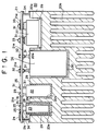
- Fig. 1 is a sectional side view of a electrical device for mounting electrical components including a thick substantially plate-shaped metal base according to this invention;
- Fig. 2 is a circuit diagram showing the circuit of a typical converter the electrical components of which are mounted on an electrical device for mounting electrical components;
- Fig. 3 is a top view of a conventional electrical device for mounting electrical components for mounting the electrical components of the circuit of Fig. 2; and
- Figs. 4 and 5 show sections along the lines A-A and B-B of Fig. 3.
- In the drawings, like reference numeral represent like or corresponding parts.
- Referring now to Fig. 1 of the drawings, an embodiment of this invention is described.
- An
aluminum metal base 20, made via aluminum die casting process, is provided, at the upper side thereof, with a plurality ofrecesses 20a for receiving and fittingly accommodating the electrical components, and, at the bottom side thereof, with radiatingfins 20b for radiating the heat generated by the electrical components. Therecesses 20a, formed at predetermined positions on themetal base 20, have dimensions corresponding to the respective heights and the shapes of the electrical components accommodated therein, such that the terminals of the electrical components are leveled, i.e., extend above the upper surface of themetal base 20 to substantially the same height. Therecesses 20a and theradiating fins 20b are formed simultaneously when themetal base 20 is cast by aluminum die casting process. - A printed
circuit board 21 having a predetermined pattern ofelectrical conductors 21a is disposed above t hemetal base 20 to make electrical connections among the electrical components accommodated in therespective recesses 20a of the metal base 20 (such as aresistor 22, acement resistor 23, aelectrolytic capacitor 26, and a power module 27 such as a power transistor module) and the electrical components disposed on the printed circuit board 21 (such as a capacitor 24). Thecement resistor 23 generating a particularly large amount of heat is enclosed in an copper covering 28. The copper covering 28 has the same form as the exterior of thecement resistor 23 and is disposed in therecess 20a such that the bottom thereof is in direct contact with themetal base 20. Thecover 28 may be made of a good heat conductive material other than copper, such as aluminum, iron, or zinc alloys. A highheat conductivity resin 29 is filled into therecesses 20a accommodating theresistor 22,cement resistor 23, and the power module 27, which generate a large amount of heat. It is noted that the high heat conductivity resin 29 fills the gap between thecement resistor 23, the copper covering 28, and therecess 20a. A resin having fluidity at the normal or elevated temperature, such as an epoxy resin, a silicone resin, an urethane resin or a polyester resin, or an mixture thereof, may be utilized as the highheat conductivity resin 29, which preferably includes, as a good heat conducting filler material, a powder made of one or a plurality of the materials selected from: copper, aluminum, silver, gold, iron, stainless steel, brass, alumina, magnesia, crystalline silica, aluminum nitride, silicon oxide, beryllia, silicon, boron nitride, zirconium silicate, silicon carbide, and diamond. - In the case of this embodiment, the high
heat conductivity resin 29 is made as follows. An amine type setting agent is added to an epoxy resin. Further, to 100 parts by weight of the epoxy resin are mixed as a filler material 900 parts by weight of alumina powder, thereby obtaining a resin having a heat conductivity at about 51×10⁻⁴ cal/cm·sec·°C. - A
heat insulating resin 30 is filled in therecess 20a accommodating theelectrolytic capacitor 26 generating a small amount of heat. A resin having fluidity at the normal or elevated temperature, such as an epoxy resin, a silicone resin, an urethane resin, or a polyester resin, or a mixture thereof, may be utilized as theheat insulating resin 30, which preferably includes a filler made of minute hollow spheres (referred to as balloon filler) that are made of one or a plurality of the materials selected from: phenol resin (phenol aldehyde resin), epoxy resin, silicone resin, urea resin (urea-formaldehyde resin), alumina, quartz sand, silica, zirconia, and glass. - In the case of this embodiment, the
heat insulating resin 30 is made as follows. An amine type setting agent is added to an epoxy resin. Further, to 100 parts by weight of the epoxy resin are mixed as balloon filler 50 parts by weight of minute hollow silica spheres, thereby obtaining a resin having a heat conductivity at about 2 X 10⁻⁴ cal/cm·sec·°C. - The electrical components accommodated in the
recesses 20a of themetal base 20 are electrically connected to the printedcircuit board 21 viaterminals 31 thereof. Theterminals 31 of theresistor 22 andcement resistor 23 are electrically connected to theelectrical conductors 21a of theprinted circuit board 21 via thesolder 25. Theterminals 31 of theelectrolytic capacitor 26 are electrically connected to theelectrical conductors 21a of theprinted circuit board 21 vianuts 32. Theterminals 31 of the power module 27 are electrically connected to theelectrical conductors 21a of theprinted circuit board 21 viafixing screws 33. The printedcircuit board 21 is supported on themetal base 20 via side supports 34 secured on themetal base 20. - The electrical device for mounting electrical components of this embodiment is assembled as follows. First, the board-mounted electrical components, the
capacitor 24, theresistor 22, and thecement resistor 23, are soldered to and fixed on the printedcircuit board 21 via thesolder 25. Thereafter, a predetermined amount of the highheat conductivity resin 29 is poured into the copper covering 28 for thecement resistor 23, and then thecement resistor 23 is encapsulated via the copper covering 28. Further, predetermined amounts of the highheat conductivity resin 29 are poured into therecesses 20a for accommodating the power module 27, theresistor 22, and thecement resistor 23, while a predetermined amount of theheat insulating resin 30 is poured into therecess 20a for accommodating theelectrolytic capacitor 26. Thereafter, the power module 27 and theelectrolytic capacitor 26 are fitted into therespective recesses 20a of themetal base 20, and the printedcircuit board 21 having mounted thereon theresistor 22 and thecement resistor 23, etc., is fixed via screws on the side supports 34 secured on themetal base 20. Furthermore, before the highheat conductivity resin 29 and theheat insulating resin 30 are set, the fixing screws 33 and the nuts 32 are fastened on theterminals 31 of the power module 27 and theelectrolytic capacitor 26, respectively. The highheat conductivity resin 29 and theheat insulating resin 30 are set by leaving them at the normal temperature or by heating them. The assembling of the electrical device for mounting electrical components is thus completed. - The electrical device for mounting electrical components according to this embodiment has the following advantages. Since the
recesses 20a are formed on themetal base 20 in accordance with the height and the exterior forms of the power module 27 and theelectrolytic capacitor 26, the horizontal and the vertical positioning of these electrical components on themetal base 20 can be accomplished accurately simply by fitting them into therespective recesses 20a. Further, there may be variations in the dimensions of the electrical components or of the gap between themetal base 20 and the printedcircuit board 21, such that the bottom ends of the electrical components, such as theresistor 22 and thecement resistor 23, screwed or soldered to the printedcircuit board 21, are not necessarily in contact with themetal base 20. However, since the resins are interposed between therecesses 20a of themetal base 20 and the electrical components such asresistor 22 and thecement resistor 23, the variations of dimensions are thereby absorbed and buffered, and the electrical components are securely fixed to themetal base 20 when the resins are set. Furthermore, since the highheat conductivity resin 29 is filled in therecesses 20a for the heat generating electrical components such as the power module 27 and theheat insulating resin 30 is filled in therecesses 20a for the non-heat generating electrical components such aselectrolytic capacitor 26, the heat generating electrical components are cooled efficiently while the intrusion of heat into the non-heat generating electrical components is effectively prevented. In addition, the electrical components generating a particularly large amount of heat, such as thecement resistor 23, are encapsulated in the copper covering 28. Thus, the heat generated in such electrical components are quickly transmitted to the copper covering 28, and from the copper covering 28 to themetal base 20, to be effectively radiated from the radiatingfins 20b of themetal base 20. - It is noted that the
metal base 20 may be made of any one of good heat conductor metals other than the diecast aluminum, such as copper, zinc alloys, or iron. Even then, substantially the same meritorious effect can be obtained.
Claims (5)
- A method of producing an electrical device for mounting electrical components which in use generate large and small amounts of heat respectively, comprising the steps of:
forming a metal base (20) having on one side thereof recesses (20a) for receiving the electrical components, said recesses having dimensions corresponding to exterior dimensions of the respective electrical components received therein, such that terminals (31) of the respective electrical components accommodated in the recesses will project to a predetermined height above the metal base;
fixing board-mounted electrical components (22, 23, 24) on a circuit board (21) carrying a pattern of electrical conductors thereon;
pouring predetermined amounts of a high heat conductivity resin (29) and a heat insulating resin (30) into respective recesses of the metal base intended to accommodate components generating large (22, 23, 27) and small (26) amounts of heat respectively;
inserting, before the resins are set, electrical components (26, 27) other than said board-mounted electrical components into respective recesses of the metal base; and
positioning, before the resins are set, said circuit board (21) above said side of the metal base having the recesses formed therein and inserting the board-mounted electrical components (22, 23, 24) carried on said circuit board into respective recesses of the metal base, terminals (31) of electrical components (26, 27) already accommodated in the recesses of the metal base coming into electrical contact with electrical conductors on the circuit board. - A method of producing of an electrical device for mounting electrical components as claimed in claim 1, wherein said forming step comprises an aluminum die casting process forming an integral metal base made of aluminum.
- A method as claimed in claim 1 or 2, wherein said terminals of the electrical components accommodated in the recesses of the metal base extend substantially to an equal height above said metal base.
- A method as claimed in claim 1, 2 or 3, wherein said metal base has fins (20b) formed integrally on a side thereof opposite to the side on which said recesses are formed, said fins radiating heat generated by electrical components accommodated in the recesses of the metal base.
- A method as claimed in claim 1, 2, 3 or 4, wherein at least one electrical component (23) generating a particularly large amount of heat is encapsulated in a cover (28) made of a good heat conductive material, and gaps between the electrical component and the cover and between the cover and the recess accommodating the electrical component are filled with said high heat conductivity resin (29).
Applications Claiming Priority (2)
| Application Number | Priority Date | Filing Date | Title |
|---|---|---|---|
| JP79503/90 | 1990-03-28 | ||
| JP2079503A JP2536657B2 (en) | 1990-03-28 | 1990-03-28 | Electric device and manufacturing method thereof |
Publications (2)
| Publication Number | Publication Date |
|---|---|
| EP0449640A1 EP0449640A1 (en) | 1991-10-02 |
| EP0449640B1 true EP0449640B1 (en) | 1994-11-09 |
Family
ID=13691739
Family Applications (1)
| Application Number | Title | Priority Date | Filing Date |
|---|---|---|---|
| EP91302781A Expired - Lifetime EP0449640B1 (en) | 1990-03-28 | 1991-03-28 | Method for mounting electrical components. |
Country Status (5)
| Country | Link |
|---|---|
| US (1) | US5373418A (en) |
| EP (1) | EP0449640B1 (en) |
| JP (1) | JP2536657B2 (en) |
| DE (1) | DE69105020T2 (en) |
| HK (1) | HK1003819A1 (en) |
Families Citing this family (111)
| Publication number | Priority date | Publication date | Assignee | Title |
|---|---|---|---|---|
| DE4237632A1 (en) * | 1992-11-07 | 1994-05-11 | Export Contor Ausenhandelsgese | Circuit arrangement |
| EP0612100B1 (en) * | 1993-02-16 | 1996-08-21 | Koninklijke Philips Electronics N.V. | Electrodeless high-pressure discharge lamp |
| EP0655881A1 (en) * | 1993-11-26 | 1995-05-31 | Siemens Aktiengesellschaft | Casing |
| FR2724283B1 (en) * | 1994-09-02 | 1996-10-18 | Schneider Electric Sa | ELECTRONIC SPEED VARIATOR |
| US5757620A (en) * | 1994-12-05 | 1998-05-26 | International Business Machines Corporation | Apparatus for cooling of chips using blind holes with customized depth |
| JP3159071B2 (en) * | 1996-08-01 | 2001-04-23 | 株式会社日立製作所 | Electric device having radiating fins |
| US5798916A (en) * | 1997-03-20 | 1998-08-25 | Electric Power Research Institute, Inc. | High power inverter pole employing series connected devices configured for reduced stray loop inductance |
| FR2766967A1 (en) * | 1997-07-31 | 1999-02-05 | Scps | THERMAL DISSIPATION AND / OR ELECTROMAGNETIC PROTECTION DEVICE FOR ELECTRONIC CARDS AND COMPONENTS |
| JPH1154971A (en) * | 1997-08-06 | 1999-02-26 | Kobe Nippon Denki Software Kk | Cooling structure of electronic device |
| JPH11121666A (en) | 1997-10-20 | 1999-04-30 | Fujitsu Ltd | Multi-chip module cooling system |
| FR2771594B1 (en) * | 1997-11-21 | 1999-12-31 | Schneider Electric Sa | ELECTRONIC SPEED VARIATOR |
| US6147869A (en) * | 1997-11-24 | 2000-11-14 | International Rectifier Corp. | Adaptable planar module |
| US5894402A (en) * | 1997-11-25 | 1999-04-13 | Pacesetter, Inc. | Electrolytic capacitor and heat sink assembly |
| DE19846156C1 (en) * | 1998-10-07 | 2000-07-27 | Bosch Gmbh Robert | Arrangement of a multi-phase converter |
| DE19850153B4 (en) * | 1998-10-30 | 2005-07-21 | Siemens Ag | Semiconductor circuit arrangement, in particular high-current converter with low DC link voltage |
| DE19919098A1 (en) * | 1998-12-15 | 2000-07-06 | Mannesmann Vdo Ag | Electronic device |
| US6195257B1 (en) * | 1999-02-13 | 2001-02-27 | Lucent Technologies Inc. | Apparatus and method of adapting a rectifier module to enhance cooling |
| DE19914497A1 (en) * | 1999-03-30 | 2000-10-19 | Siemens Ag | Heat-removal metal base arrangement for circuit board especially ceramic substrate |
| JP2001054286A (en) * | 1999-08-06 | 2001-02-23 | Mitsubishi Electric Corp | Electronic control board |
| DE10009398C2 (en) | 2000-02-28 | 2002-03-14 | Epcos Ag | Heatsink module and arrangement of heatsink modules |
| JP4009056B2 (en) * | 2000-05-25 | 2007-11-14 | 三菱電機株式会社 | Power module |
| DE10138711B4 (en) * | 2000-10-02 | 2009-12-31 | Siemens Ag | Cooling arrangement for arranged in a housing loss heat generating electrical components and electrical device with such a cooling arrangement |
| US6631071B2 (en) * | 2002-01-16 | 2003-10-07 | Matsushita Electric Industrial Co., Ltd. | Capacitor module |
| JP3611548B2 (en) * | 2002-02-20 | 2005-01-19 | Tdk株式会社 | Switching power supply and manufacturing method thereof |
| FI20021232A0 (en) * | 2002-06-24 | 2002-06-24 | Nokia Corp | Method for manufacturing an electronic unit for a radio system and an electronic unit |
| US7057896B2 (en) | 2002-08-21 | 2006-06-06 | Matsushita Electric Industrial Co., Ltd. | Power module and production method thereof |
| GB0221123D0 (en) * | 2002-09-12 | 2002-10-23 | Bae Systems Plc | Improvements in or relating to cooling of electronic components |
| US6781834B2 (en) * | 2003-01-24 | 2004-08-24 | Hewlett-Packard Development Company, L.P. | Cooling device with air shower |
| US7027300B2 (en) * | 2003-09-16 | 2006-04-11 | Mobility Electronics, Inc. | Compact electronics plenum |
| EP1589547A4 (en) * | 2003-09-18 | 2009-11-25 | Panasonic Corp | CAPACITOR BLOCK |
| US20050257913A1 (en) * | 2004-05-21 | 2005-11-24 | Acroman Co., Ltd. | Heat sink with fins fitted and bonded thereto by applying conductive glue |
| DE102004047182A1 (en) * | 2004-09-29 | 2006-03-30 | Robert Bosch Gmbh | Electronic device with a multilayer ceramic substrate |
| GB2419463A (en) * | 2004-10-25 | 2006-04-26 | Elan House Ltd | Heat sink |
| US7365273B2 (en) * | 2004-12-03 | 2008-04-29 | Delphi Technologies, Inc. | Thermal management of surface-mount circuit devices |
| FR2881018B1 (en) * | 2005-01-19 | 2007-04-06 | Intelligent Electronic Systems | METHOD FOR COOLING A STATIC POWER CONVERSION DEVICE AND CORRESPONDING DEVICE |
| US7310233B2 (en) * | 2005-01-28 | 2007-12-18 | Tyco Electronics Power Systems | Apparatus and method for transferring heat from an electrical module |
| WO2006095436A1 (en) * | 2005-03-11 | 2006-09-14 | Fujitsu Limited | Heat absorption member, cooling device, and electronic apparatus |
| JP2007012941A (en) * | 2005-06-30 | 2007-01-18 | Toshiba Corp | Electronic device and heat sink incorporated in the electronic device |
| DE102005034546A1 (en) * | 2005-07-23 | 2007-01-25 | Conti Temic Microelectronic Gmbh | Module with cooling device, has melt-body retained in number of cooling chambers |
| DE102005036299B4 (en) * | 2005-08-02 | 2008-01-24 | Siemens Ag | cooling arrangement |
| ES2655254T3 (en) * | 2006-01-16 | 2018-02-19 | Mitsubishi Electric Corporation | Motor control circuit and outdoor unit of air conditioner |
| US7450387B2 (en) * | 2006-03-02 | 2008-11-11 | Tdk Innoveta Technologies, Inc. | System for cooling electronic components |
| DE102006061215A1 (en) * | 2006-08-12 | 2008-02-21 | Diehl Ako Stiftung & Co. Kg | Power electronics with heat sink |
| ES2504515T3 (en) * | 2007-05-25 | 2014-10-08 | Sma Solar Technology Ag | Investor Housing |
| TWM331763U (en) * | 2007-11-14 | 2008-05-01 | Simplo Technology Co Ltd | A PCB with advanced soldering holes and the same implemented on a battery set |
| US7791887B2 (en) * | 2008-02-12 | 2010-09-07 | Honeywell International Inc. | Contour surface cooling of electronics devices |
| US8017451B2 (en) | 2008-04-04 | 2011-09-13 | The Charles Stark Draper Laboratory, Inc. | Electronic modules and methods for forming the same |
| US8273603B2 (en) * | 2008-04-04 | 2012-09-25 | The Charles Stark Draper Laboratory, Inc. | Interposers, electronic modules, and methods for forming the same |
| DE102008023714B4 (en) * | 2008-05-15 | 2011-01-20 | Semikron Elektronik Gmbh & Co. Kg | Arrangement with a main carrier and a printed circuit board with components |
| DE102009044368B4 (en) * | 2009-10-30 | 2014-07-03 | Lear Corporation Gmbh | cooling arrangement |
| DE102010028927A1 (en) * | 2010-05-12 | 2011-11-17 | Zf Friedrichshafen Ag | Power electronics arrangement |
| DE102010043445B3 (en) * | 2010-11-05 | 2012-04-19 | Semikron Elektronik Gmbh & Co. Kg | Capacitor assembly for power electronic apparatus, has spacer and electrical isolating capping material that are arranged such that capacitor is in non contact with metal structure |
| ITUD20110040A1 (en) * | 2011-03-15 | 2012-09-16 | Eurotech S P A | LIQUID COOLING DEVICE OF ELECTRONIC BOARDS |
| US9317079B2 (en) * | 2011-03-29 | 2016-04-19 | Echostar Uk Holdings Limited | Media content device with customized panel |
| DE102011006632A1 (en) * | 2011-04-01 | 2012-10-04 | Robert Bosch Gmbh | electronic module |
| DE102011076325B4 (en) * | 2011-05-24 | 2016-05-04 | Semikron Elektronik Gmbh & Co. Kg | Cooling arrangement for a power electronic component with subsystems and a cooling device |
| DE102011081283A1 (en) * | 2011-08-19 | 2013-02-21 | Robert Bosch Gmbh | Capacitor with a heat sink |
| JP5693419B2 (en) * | 2011-08-31 | 2015-04-01 | 三菱電機株式会社 | Electrical equipment housing |
| CN103090338B (en) * | 2011-11-03 | 2018-10-09 | 欧司朗股份有限公司 | Actuator assembly and its manufacturing method |
| EP2637489B1 (en) * | 2012-03-06 | 2018-01-24 | ABB Schweiz AG | Electrical power circuit assembly |
| CN104335471B (en) * | 2012-05-23 | 2017-11-10 | 三菱电机株式会社 | Inverter unit |
| US10392959B2 (en) * | 2012-06-05 | 2019-08-27 | General Electric Company | High temperature flame sensor |
| JP5992235B2 (en) * | 2012-07-11 | 2016-09-14 | 東芝機械株式会社 | Control device |
| JP6145717B2 (en) * | 2012-11-21 | 2017-06-14 | パナソニックIpマネジメント株式会社 | Power converter |
| CN103002722B (en) * | 2012-12-18 | 2015-03-25 | 武汉光迅科技股份有限公司 | Heat control device for power equipment |
| JP6166081B2 (en) * | 2013-03-28 | 2017-07-19 | 株式会社ケーヒン | Electronic control device for vehicle |
| CN109166711A (en) * | 2013-06-10 | 2019-01-08 | 施耐德电气太阳能逆变器美国股份有限公司 | Electronic system and forming method thereof |
| US20150029668A1 (en) * | 2013-07-24 | 2015-01-29 | Aura Systems, Inc. | Clamping Structure for Power Electronic Components |
| JP6209737B2 (en) * | 2013-08-30 | 2017-10-11 | パナソニックIpマネジメント株式会社 | Inverter device |
| JP6169181B2 (en) * | 2013-10-07 | 2017-07-26 | 日立オートモティブシステムズ株式会社 | DC-DC converter device |
| JP2015082951A (en) * | 2013-10-24 | 2015-04-27 | トヨタ自動車株式会社 | Electric power conversion system |
| JP2015088556A (en) * | 2013-10-29 | 2015-05-07 | 富士電機株式会社 | Electronic module |
| CN104682722B (en) * | 2013-11-26 | 2018-01-26 | 台达电子企业管理(上海)有限公司 | Power conversion device and assembly method thereof |
| JP2015126590A (en) * | 2013-12-26 | 2015-07-06 | パナソニックIpマネジメント株式会社 | Power converter |
| JP6335515B2 (en) * | 2014-01-15 | 2018-05-30 | 三菱電機株式会社 | Protective structure of semiconductor element and outdoor unit of air conditioner |
| JP6269094B2 (en) * | 2014-01-20 | 2018-01-31 | Tdk株式会社 | Power supply |
| JP6326618B2 (en) * | 2014-01-31 | 2018-05-23 | パナソニックIpマネジメント株式会社 | Power converter |
| JP2015198168A (en) * | 2014-04-01 | 2015-11-09 | 富士電機株式会社 | Electronic device, power conversion device and rotating electric machine |
| DE102014211206B3 (en) * | 2014-06-12 | 2015-09-10 | Continental Automotive Gmbh | Device having a printed circuit board and an electronic circuit arranged thereon, which has an electrolytic capacitor whose operating temperature can be regulated by means of the electronic circuit |
| US11191186B2 (en) * | 2014-06-24 | 2021-11-30 | David Lane Smith | System and method for fluid cooling of electronic devices installed in an enclosure |
| US10064310B2 (en) * | 2014-06-25 | 2018-08-28 | Hitachi, Ltd. | Power-module device, power conversion device, and method for manufacturing power-module device |
| JP2016071269A (en) * | 2014-09-30 | 2016-05-09 | 株式会社東芝 | Electronic device and system |
| US10199804B2 (en) * | 2014-12-01 | 2019-02-05 | Tesla, Inc. | Busbar locating component |
| US9536671B2 (en) | 2014-12-01 | 2017-01-03 | Telsa Motors, Inc. | Planar capacitor terminals |
| JP2016178141A (en) * | 2015-03-19 | 2016-10-06 | パナソニックIpマネジメント株式会社 | Heat sink |
| JP6693706B2 (en) * | 2015-04-06 | 2020-05-13 | 株式会社デンソー | Electronic control unit |
| JP6701637B2 (en) * | 2015-07-21 | 2020-05-27 | ダイキン工業株式会社 | Inverter device |
| JP6528620B2 (en) * | 2015-09-15 | 2019-06-12 | 株式会社オートネットワーク技術研究所 | Circuit structure and electrical connection box |
| JP6453195B2 (en) * | 2015-09-29 | 2019-01-16 | 日立オートモティブシステムズ株式会社 | In-vehicle control device |
| DE102015226149A1 (en) * | 2015-12-21 | 2017-06-22 | Robert Bosch Gmbh | Drive electronics for a drive |
| JP2017192285A (en) * | 2016-04-11 | 2017-10-19 | 三菱電機株式会社 | Rotary machine and vehicle including the same |
| CN106206330B (en) * | 2016-08-26 | 2019-02-26 | 王文杰 | A pin-type power single-tube integrated structure applied to electric vehicle electronic control products |
| WO2018088162A1 (en) * | 2016-11-11 | 2018-05-17 | 日本精工株式会社 | Electronic control device and steering device |
| CN108630636B (en) * | 2017-03-24 | 2022-01-14 | 德昌电机(深圳)有限公司 | MOS device mounting structure, controller and electric power steering system |
| JP2018186143A (en) * | 2017-04-25 | 2018-11-22 | オムロンオートモーティブエレクトロニクス株式会社 | Circuit board module, electronic device |
| JP2018190913A (en) * | 2017-05-11 | 2018-11-29 | 株式会社オートネットワーク技術研究所 | Storage element connection structure and storage module |
| CN109951055A (en) * | 2017-12-19 | 2019-06-28 | 法雷奥动力总成(上海)有限公司 | Electric pressure converter and its assemble method |
| DE112018007612T5 (en) | 2018-05-14 | 2021-02-04 | Mitsubishi Electric Corporation | Power conversion device |
| JP7314478B2 (en) * | 2018-05-18 | 2023-07-26 | 住友電気工業株式会社 | Device with electrical circuit board |
| US10667439B1 (en) * | 2018-11-01 | 2020-05-26 | Franklin Electric Company, Inc. | Discrete power component assembly |
| US11057985B2 (en) * | 2019-02-28 | 2021-07-06 | Denso Ten Limited | Printed wiring board |
| US11439043B2 (en) * | 2019-05-20 | 2022-09-06 | International Business Machines Corporation | Multi-device cooling structure having assembly alignment features |
| JP2020198347A (en) * | 2019-05-31 | 2020-12-10 | 株式会社豊田自動織機 | Power conversion apparatus |
| US11917797B2 (en) * | 2019-12-03 | 2024-02-27 | The Florida State University Research Foundation, Inc. | Integrated thermal-electrical component for power electronics converters |
| JP6854936B1 (en) * | 2020-01-20 | 2021-04-07 | 三菱電機株式会社 | Rotating machine |
| JP7069238B2 (en) | 2020-03-17 | 2022-05-17 | 株式会社クボタ | Electronic control device |
| DE102020117310A1 (en) | 2020-07-01 | 2022-01-05 | Seg Automotive Germany Gmbh | Power converter for electric machine and electric machine |
| JP7208550B2 (en) * | 2021-03-30 | 2023-01-19 | ダイキン工業株式会社 | Electrical equipment and refrigeration equipment |
| JP7098025B1 (en) * | 2021-06-09 | 2022-07-08 | 三菱電機株式会社 | Power converter |
| US12588508B2 (en) * | 2022-12-20 | 2026-03-24 | Qualcomm Incorporated | Package comprising a lid structure with a compartment |
| WO2025190574A1 (en) | 2024-03-11 | 2025-09-18 | Sew-Eurodrive Gmbh & Co Kg | Electrical device |
Family Cites Families (12)
| Publication number | Priority date | Publication date | Assignee | Title |
|---|---|---|---|---|
| US3018424A (en) * | 1959-05-28 | 1962-01-23 | Westinghouse Electric Corp | Rectifier apparatus |
| GB1441692A (en) * | 1973-11-27 | 1976-07-07 | Siemens Ag | Module accomodating a disc-shaped rectifier element |
| DE2919058A1 (en) * | 1979-05-10 | 1980-11-20 | Siemens Ag | Electronic appliance with printed circuit module - encapsulated with modules in recesses of precast plastic block |
| JPS59146981A (en) * | 1983-02-09 | 1984-08-23 | 日本碍子株式会社 | Silicon nitride sintered body and manufacture |
| DE3307654A1 (en) * | 1983-03-04 | 1984-09-06 | Robert Bosch Gmbh, 7000 Stuttgart | Electric switchgear in vehicular engine compartment - has cooling intermediate bottom with notch for electric component to be cooled |
| JPS60151186A (en) * | 1984-01-17 | 1985-08-09 | Iseki & Co Ltd | Safety frame fitting device of tractor |
| JPH079952B2 (en) * | 1985-07-31 | 1995-02-01 | 沖電気工業株式会社 | Circuit board for resin encapsulation |
| US4872102A (en) * | 1986-04-28 | 1989-10-03 | Dimensions Unlimited, Inc. | D.C. to A.C. inverter having improved structure providing improved thermal dissipation |
| JPH0680911B2 (en) * | 1986-05-08 | 1994-10-12 | 富士通株式会社 | Heat dissipation structure of printed wiring board with electronic components |
| US4918571A (en) * | 1987-03-31 | 1990-04-17 | Amp Incorporated | Chip carrier with energy storage means |
| JPS6422093U (en) * | 1987-07-29 | 1989-02-03 | ||
| DE4009445A1 (en) * | 1989-04-20 | 1990-10-25 | Siemens Ag | COOLING DEVICE FOR ELECTRONIC ASSEMBLIES OF A ASSEMBLED CIRCUIT BOARD |
-
1990
- 1990-03-28 JP JP2079503A patent/JP2536657B2/en not_active Expired - Fee Related
-
1991
- 1991-03-26 US US07/675,202 patent/US5373418A/en not_active Expired - Lifetime
- 1991-03-28 EP EP91302781A patent/EP0449640B1/en not_active Expired - Lifetime
- 1991-03-28 DE DE69105020T patent/DE69105020T2/en not_active Expired - Fee Related
-
1998
- 1998-04-09 HK HK98103009A patent/HK1003819A1/en not_active IP Right Cessation
Also Published As
| Publication number | Publication date |
|---|---|
| JP2536657B2 (en) | 1996-09-18 |
| DE69105020D1 (en) | 1994-12-15 |
| EP0449640A1 (en) | 1991-10-02 |
| HK1003819A1 (en) | 1998-11-06 |
| DE69105020T2 (en) | 1995-06-22 |
| JPH03278596A (en) | 1991-12-10 |
| US5373418A (en) | 1994-12-13 |
Similar Documents
| Publication | Publication Date | Title |
|---|---|---|
| EP0449640B1 (en) | Method for mounting electrical components. | |
| HK1003819B (en) | Method for mounting electrical components | |
| US6313598B1 (en) | Power semiconductor module and motor drive system | |
| US6282092B1 (en) | Electronic circuit device and method of fabricating the same | |
| JP3241639B2 (en) | Multi-chip module cooling structure and method of manufacturing the same | |
| US20030011054A1 (en) | Power module package having improved heat dissipating capability | |
| JPH09321395A (en) | Heat dissipation board for mounting electronic parts and manufacturing method thereof | |
| EP0528291A2 (en) | Semiconductor chip module and method for manufacturing the same | |
| JP4437860B2 (en) | Wiring block storage structure | |
| JPH05218233A (en) | Semiconductor device and manufacturing method thereof | |
| JPH0245357B2 (en) | ||
| EP0812015A1 (en) | A heat dissipator for integrated circuits | |
| CN113853737B (en) | Power conversion device and method for manufacturing the same | |
| US5757619A (en) | Cooling apparatus for electronic components | |
| CN116705720B (en) | A power module and its packaging method | |
| US6483706B2 (en) | Heat dissipation for electronic components | |
| JPH1022435A (en) | Semiconductor device and manufacturing method thereof | |
| US3476981A (en) | Miniature power circuit assembly | |
| JPH0922970A (en) | Electronic components | |
| JPH05343607A (en) | Hybrid integrated circuit device | |
| JPH0818182A (en) | Circuit board | |
| EP0782184A1 (en) | Heat dissipating and supporting structure for a package | |
| JPS6151427B2 (en) | ||
| JP2680764B2 (en) | Hybrid integrated circuit and manufacturing method thereof | |
| JPS63136655A (en) | Chip carrier |
Legal Events
| Date | Code | Title | Description |
|---|---|---|---|
| PUAI | Public reference made under article 153(3) epc to a published international application that has entered the european phase |
Free format text: ORIGINAL CODE: 0009012 |
|
| AK | Designated contracting states |
Kind code of ref document: A1 Designated state(s): DE FR GB |
|
| 17P | Request for examination filed |
Effective date: 19911104 |
|
| 17Q | First examination report despatched |
Effective date: 19930716 |
|
| GRAA | (expected) grant |
Free format text: ORIGINAL CODE: 0009210 |
|
| AK | Designated contracting states |
Kind code of ref document: B1 Designated state(s): DE FR GB |
|
| PG25 | Lapsed in a contracting state [announced via postgrant information from national office to epo] |
Ref country code: FR Effective date: 19941109 |
|
| REF | Corresponds to: |
Ref document number: 69105020 Country of ref document: DE Date of ref document: 19941215 |
|
| REG | Reference to a national code |
Ref country code: GB Ref legal event code: 727 |
|
| REG | Reference to a national code |
Ref country code: GB Ref legal event code: 727A |
|
| EN | Fr: translation not filed | ||
| REG | Reference to a national code |
Ref country code: GB Ref legal event code: 727B |
|
| PLBE | No opposition filed within time limit |
Free format text: ORIGINAL CODE: 0009261 |
|
| STAA | Information on the status of an ep patent application or granted ep patent |
Free format text: STATUS: NO OPPOSITION FILED WITHIN TIME LIMIT |
|
| REG | Reference to a national code |
Ref country code: GB Ref legal event code: SP |
|
| 26N | No opposition filed | ||
| REG | Reference to a national code |
Ref country code: GB Ref legal event code: 746 Effective date: 19951106 |
|
| PGFP | Annual fee paid to national office [announced via postgrant information from national office to epo] |
Ref country code: GB Payment date: 19980319 Year of fee payment: 8 |
|
| PGFP | Annual fee paid to national office [announced via postgrant information from national office to epo] |
Ref country code: DE Payment date: 19980403 Year of fee payment: 8 |
|
| PG25 | Lapsed in a contracting state [announced via postgrant information from national office to epo] |
Ref country code: GB Free format text: LAPSE BECAUSE OF NON-PAYMENT OF DUE FEES Effective date: 19990328 |
|
| GBPC | Gb: european patent ceased through non-payment of renewal fee |
Effective date: 19990328 |
|
| PG25 | Lapsed in a contracting state [announced via postgrant information from national office to epo] |
Ref country code: DE Free format text: LAPSE BECAUSE OF NON-PAYMENT OF DUE FEES Effective date: 20000101 |