EP0449659A1 - Linearisierter Tri-State-Phasendetektor - Google Patents
Linearisierter Tri-State-Phasendetektor Download PDFInfo
- Publication number
- EP0449659A1 EP0449659A1 EP91302829A EP91302829A EP0449659A1 EP 0449659 A1 EP0449659 A1 EP 0449659A1 EP 91302829 A EP91302829 A EP 91302829A EP 91302829 A EP91302829 A EP 91302829A EP 0449659 A1 EP0449659 A1 EP 0449659A1
- Authority
- EP
- European Patent Office
- Prior art keywords
- output
- input
- coupled
- storage means
- flip
- Prior art date
- Legal status (The legal status is an assumption and is not a legal conclusion. Google has not performed a legal analysis and makes no representation as to the accuracy of the status listed.)
- Granted
Links
- 238000001514 detection method Methods 0.000 claims description 18
- 238000012358 sourcing Methods 0.000 claims 6
- 238000010586 diagram Methods 0.000 description 4
- 230000003111 delayed effect Effects 0.000 description 3
- 229920000729 poly(L-lysine) polymer Polymers 0.000 description 3
- 230000018199 S phase Effects 0.000 description 1
- 239000002131 composite material Substances 0.000 description 1
- 230000001934 delay Effects 0.000 description 1
- 230000000694 effects Effects 0.000 description 1
- 230000000630 rising effect Effects 0.000 description 1
- 239000007787 solid Substances 0.000 description 1
- 230000003595 spectral effect Effects 0.000 description 1
Images

Classifications
-
- H—ELECTRICITY
- H03—ELECTRONIC CIRCUITRY
- H03D—DEMODULATION OR TRANSFERENCE OF MODULATION FROM ONE CARRIER TO ANOTHER
- H03D13/00—Circuits for comparing the phase or frequency of two mutually-independent oscillations
- H03D13/003—Circuits for comparing the phase or frequency of two mutually-independent oscillations in which both oscillations are converted by logic means into pulses which are applied to filtering or integrating means
- H03D13/004—Circuits for comparing the phase or frequency of two mutually-independent oscillations in which both oscillations are converted by logic means into pulses which are applied to filtering or integrating means the logic means delivering pulses at more than one terminal, e.g. up and down pulses
-
- H—ELECTRICITY
- H03—ELECTRONIC CIRCUITRY
- H03L—AUTOMATIC CONTROL, STARTING, SYNCHRONISATION OR STABILISATION OF GENERATORS OF ELECTRONIC OSCILLATIONS OR PULSES
- H03L7/00—Automatic control of frequency or phase; Synchronisation
- H03L7/06—Automatic control of frequency or phase; Synchronisation using a reference signal applied to a frequency- or phase-locked loop
- H03L7/08—Details of the phase-locked loop
- H03L7/085—Details of the phase-locked loop concerning mainly the frequency- or phase-detection arrangement including the filtering or amplification of its output signal
- H03L7/089—Details of the phase-locked loop concerning mainly the frequency- or phase-detection arrangement including the filtering or amplification of its output signal the phase or frequency detector generating up-down pulses
- H03L7/0891—Details of the phase-locked loop concerning mainly the frequency- or phase-detection arrangement including the filtering or amplification of its output signal the phase or frequency detector generating up-down pulses the up-down pulses controlling source and sink current generators, e.g. a charge pump
Definitions
- the present invention relates to phase detection circuits as may be used in phase locked loops.
- Phase detection circuits are typically used to detect a phase difference between two signals. These circuits can be used in phase locked loops (PLL) to detect a difference between a reference signal generated by a reference oscillator and a loop feedback signal. The output of the phase detection circuit is then used to produce a fixed phase relationship between the PLL output signal and the input reference signal. PLLs are discussed in H. Krauss, C. Bostian, and F. Raab, Solid State Radio Engineering at Chapter 6 (1980).
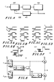
- a typical three state phase detector circuit is illustrated in Figure 1.
- the D inputs to both flip-flops is tied to a logic high.
- the reference signal of reference frequency F r clocks one flip-flop and the loop feedback signal of variable frequency F v clocks the other flip-flop.
- the outputs of the flip-flops are input to an AND gate.
- the output of the AND gate is input to a delay element the output of which is connected to the reset inputs of the flip-flops.
- the delay element causes the outputs of the flip-flops to have a minimum pulse width, even during a zero phase error condition.
- the outputs of the flip-flops also each enable a charge pump.
- the charge pumps are connected at a common node that is the output of the circuit.
- the circuit operates by the F r and F v signals clocking in the logic high from the flip-flop inputs. If F r leads F v , as illustrated in Figure 2A, the positive polarity charge pump is turned on by the output from that D flip-flop causing a positive pulse to be output from the circuit. The width of the net output pulse is the difference between the time the F r flip-flop is clocked to the time the F v flip-flop is clocked.
- the inputs to the AND gate will both be a logic one causing the output of the AND gate to be a logic one, thereby reseting the flip-flops after a delay, turning off the charge pumps and ending the output pulses from the flip-flops.
- the output of this circuit is low pass filtered before driving a voltage controlled oscillator, the frequency divided output of which is the loop feedback signal.
- phase detection circuits used in PLLs typically have a linear transfer function. Around the zero phase error region, however, there can exist a non-linear transfer function of phase to current or charge. This non-linearity degrades the spectral purity of the PLLs signal, especially when used with fractional division, by increasing the amplitude of the sidebands at subharmonics and harmonics of the output frequency resolution. See Martin, U.S. Patent No. 4,816,774 assigned to Motorola, for a discussion on output frequency resolution. There is a resulting need for a phase detection circuit that has a more linear transfer function of phase to current or charge for small phase differences, thereby attenuating these sidebands.
- phase detecting apparatus is provied as definent by the claims.
- the apparatus has the advantage of providing linear phase detection for small phase differences.
- a preferred embodiment of the invention is comprised of two D type flip-flops, an AND gate, and a delay element.
- the inputs to the D flip-flops are tied to a logic high.
- the first flip-flop is clocked with a reference signal while the other flip-flop is clocked with a feedback signal, typically from a voltage controlled oscillator in a phase locked loop.
- the outputs of the flip-flops are ANDed together with the result of this operation going through a delay element before reseting one of the flip-flops.
- the other flip-flop is reset by the output of the AND gate without the delay element.
- Each flip-flop output enables a charge pump - one negative polarity and one positive polarity.
- the present invention will maintain a lock condition in a phase locked loop by extending the DOWN pulse enabling the negative polarity charge pump to the same width as the UP pulse that enables the positive pump. This will create a net zero charge from the present invention.
- Figure 1 shows a prior art phase detection circuit.
- FIGS. 1A, 2B, 2C show timing diagrams generated by the prior art phase detection circuit shown in Figure 1.
- Figure 3 shows a block diagram of the preferred embodiment of the present invention.
- Figure 4 shows a block diagram of the preferred embodiment as used in a phase locked loop.
- Figures 5A, 5B, 5C, 5D, 5E, and 5F show timing diagrams generated by the preferred embodiment.
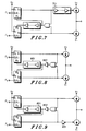
- Figure 6 shows an alternate embodiment of the present invention.
- FIG. 7 shows another alternate embodiment of the present invention.
- FIG 8 shows yet another alternate embodiment of the present invention.
- FIG. 9 shows yet another alternate embodiment of the present invention.
- Figure 10 shows a plot of the transfer function for the prior art and the preferred embodiment of the present invention.
- the present invention detects phase differences between two signals, and is particularly useful in detecting small phase differences while maintaining a substantially linear transfer function of phase to current or charge.
- the present invention is used for phase detection in phase locked loops (PLL).
- the preferred embodiment (300) is comprised of two D type flip-flops (301 and 302), an AND gate (303), and a delay element (304).
- the flip-flops (301 and 302), with their D inputs tied to a logic high, are clocked by two separate signals. One is clocked by a reference signal having a frequency F r and the other is clocked by a variable frequency signal F v . If the apparatus (300) is used in a PLL (400), as illustrated in Figure 4, F r is generated by a reference oscillator and F v is the loop feedback output of the frequency divider (401).
- the outputs of the flip-flops (301 and 302) are ANDed and the resulting AND gate (303) output delayed by the delay element (304).
- the output of the delay element (304) is used to reset one of the flip-flops (301) while the output from the AND gate (303) prior to the delay element (304) resets the other flip-flop (302); it is irrelevant which flip-flop (301 or 302) gets reset by the delayed AND gate (303) output.
- Each of the flip-flop outputs is used to enable a charge pump - a negative polarity source (306) and a positive polarity source (305).
- the output of the apparatus (300) is the common node between the two charge pumps (305 and 306).
- the apparatus (300) operates by the F r and F v signals clocking in the logic high from the flip-flop inputs.
- the F v signal clocks the F v flip-flop (302) to a high state causing a high pulse on the DOWN line.
- the F r signal clocks the F r flip-flop (301) to a high state causing a high pulse on the UP line.
- These pulses enable the negative and positive polarity charge pumps (305 and 306) respectively.
- the width of any negative pulse will be the difference between the time the F v flip-flop (302) is clocked to the time the F r flip-flop (301) is clocked by the rising edge of F r .
- the negative output pulse is wider than the positive output pulse; the positive output pulse having a width of T delay .
- the net current produced by the present invention, integrated over both pulses, is negative.
- the negative output pulse is narrower than the positive output pulse; the positive output pulse having a width of T delay .
- the net current produced by the present invention in this case, integrated over both pulses, is positive.
- the inherent delay of the flip-flops (301 and 302) and AND gate (303) will make the width of the positive pulse slightly more than T delay and the negative pulse will be active slightly beyond when F r goes high. This does not result in behavior any different from the idealized case previously described except that the positive and negative pulses overlap for a time equal to the inherent delay of the flip-flops (301 and 302) and AND gate (303).
- the DOWN pulse extends to the same width as the UP pulse, creating a net zero charge from the pump.
- the DOWN pulse will always lead the UP pulse in phase by T delay .
- Any phase modulation in the PLL is done by the leading edge (501) of the DOWN pulse, as seen by the moving leading edge (501), as long as the DOWN pulse width is maintained greater than PW minDOWN as shown in Figure 5E. This, in effect, produces a fixed phase error between F r and F v .
- the remaining non-linearity in the present invention will be due to the DOWN path alone and will be small if the modulation is small compared to PW minUP .
- the composite current output of the apparatus (300) produced by summing the UP/DOWN pulses in opposite phase, as illustrated in Figure 5F, will produce reference spurs that will modulate the VCO (402) in the PLL (400). While this will be acceptable in many applications, some applications will not accept this.
- a delay element (601 and 701) of delay T delay can be inserted in the path of the flip-flop that is being reset with the AND gate output that is not delayed. This delay will bring the two pulses from the flip-flops back into phase, thereby eliminating any induced VCO modulation caused by non-overlapping pulses.
- An alternate embodiment can also have a delay (801 and 802) in both reset signals, as illustrated in Figure 8.
- Yet another alternate embodiment illustrated in Figure 9, utilizes a delay (901) of T delay in the DOWN path to bring the two pulses from the flip-flops into phase.
- Figure 10 illustrates both the prior art's phase to charge transfer function (1001) and the phase to charge transfer function (1002) of the preferred embodiment of the invention.
- the prior art transfer function (1001) is non-linear at the zero phase error region while the present invention transfer function (1002) is linear in this region.
- the present invention has been shown to detect small phase differences between two signals.
- the present invention when used in a PLL having fractional division, will maintain a linear transfer function of phase to current or charge at and around the zero phase error region.
Landscapes
- Engineering & Computer Science (AREA)
- Power Engineering (AREA)
- Stabilization Of Oscillater, Synchronisation, Frequency Synthesizers (AREA)
- Indication And Recording Devices For Special Purposes And Tariff Metering Devices (AREA)
- Manipulation Of Pulses (AREA)
Applications Claiming Priority (2)
| Application Number | Priority Date | Filing Date | Title |
|---|---|---|---|
| US07/500,626 US4970475A (en) | 1990-03-28 | 1990-03-28 | Linearized three state phase detector |
| US500626 | 1990-03-28 |
Publications (2)
| Publication Number | Publication Date |
|---|---|
| EP0449659A1 true EP0449659A1 (de) | 1991-10-02 |
| EP0449659B1 EP0449659B1 (de) | 1995-09-20 |
Family
ID=23990247
Family Applications (1)
| Application Number | Title | Priority Date | Filing Date |
|---|---|---|---|
| EP91302829A Expired - Lifetime EP0449659B1 (de) | 1990-03-28 | 1991-03-28 | Linearisierter Tri-State-Phasendetektor |
Country Status (5)
| Country | Link |
|---|---|
| US (1) | US4970475A (de) |
| EP (1) | EP0449659B1 (de) |
| AT (1) | ATE128292T1 (de) |
| CA (1) | CA2036314C (de) |
| DE (1) | DE69113091T2 (de) |
Families Citing this family (31)
| Publication number | Priority date | Publication date | Assignee | Title |
|---|---|---|---|---|
| US5252865A (en) * | 1991-08-22 | 1993-10-12 | Triquint Semiconductor, Inc. | Integrating phase detector |
| DE4139117C1 (de) * | 1991-11-28 | 1993-06-09 | Texas Instruments Deutschland Gmbh, 8050 Freising, De | |
| US5397928A (en) * | 1992-01-17 | 1995-03-14 | Sipex Corporation | Voltage tripler using a charge pump having a single multiplexed charge transfer capacitor |
| US5306954A (en) * | 1992-06-04 | 1994-04-26 | Sipex Corporation | Charge pump with symmetrical +V and -V outputs |
| US5754080A (en) * | 1993-12-20 | 1998-05-19 | At&T Global Information Solutions Company | Single-edge triggered phase detector |
| EP0665650A1 (de) * | 1994-01-31 | 1995-08-02 | STMicroelectronics S.A. | Hochgeschwindigkeitsniederspannungsphasendetektor |
| FR2717019A1 (fr) * | 1994-03-02 | 1995-09-08 | Philips Composants | Dispositif oscillateur verrouillé en phase. |
| KR960006292A (ko) * | 1994-07-28 | 1996-02-23 | 사또 겐이찌로 | 주파수위상비교기 |
| US6404247B1 (en) * | 1995-11-13 | 2002-06-11 | Industrial Technology Research Institute | All digital phase-locked loop |
| US5760637A (en) * | 1995-12-11 | 1998-06-02 | Sipex Corporation | Programmable charge pump |
| US5815041A (en) * | 1996-04-12 | 1998-09-29 | Silicon Image, Inc. | High-speed and high-precision phase locked loop having phase detector with dynamic logic structure |
| US5661419A (en) * | 1996-05-23 | 1997-08-26 | Sun Microsystems, Inc. | Dynamic phase-frequency detector circuit |
| US5963058A (en) * | 1997-03-19 | 1999-10-05 | Intel Corporation | Phase frequency detector |
| US5966033A (en) * | 1998-01-27 | 1999-10-12 | Credence Systems Corporation | Low ripple phase detector |
| US6049233A (en) * | 1998-03-17 | 2000-04-11 | Motorola, Inc. | Phase detection apparatus |
| US6150889A (en) * | 1998-08-03 | 2000-11-21 | Motorola, Inc. | Circuit and method for minimizing recovery time |
| US6002273A (en) * | 1998-10-05 | 1999-12-14 | Motorola, Inc. | Linear low noise phase-frequency detector |
| US6100721A (en) * | 1999-02-01 | 2000-08-08 | Motorola, Inc. | Circuit and method of extending the linear range of a phase frequency detector |
| US6326826B1 (en) | 1999-05-27 | 2001-12-04 | Silicon Image, Inc. | Wide frequency-range delay-locked loop circuit |
| US6798858B1 (en) | 2000-02-04 | 2004-09-28 | International Business Machines Corporation | Lock detector for delay or phase locked loops |
| US7042970B1 (en) * | 2001-06-15 | 2006-05-09 | Analog Devices, Inc. | Phase frequency detector with adjustable offset |
| US6771096B1 (en) * | 2002-03-25 | 2004-08-03 | Cypress Semiconductor Corp. | Circuit, system, and method for using hysteresis to avoid dead zone or non-linear conditions in a phase frequency detector |
| US6756822B1 (en) | 2002-10-31 | 2004-06-29 | Xilinx, Inc. | Phase detector employing asynchronous level-mode sequential circuitry |
| US6941116B2 (en) * | 2002-11-27 | 2005-09-06 | Broadcom Corp. | Linearization technique for phase locked loops employing differential charge pump circuitry |
| JP3737800B2 (ja) * | 2002-12-25 | 2006-01-25 | 株式会社東芝 | 同期化回路 |
| US6946887B2 (en) * | 2003-11-25 | 2005-09-20 | International Business Machines Corporation | Phase frequency detector with programmable minimum pulse width |
| US7400204B2 (en) * | 2004-06-28 | 2008-07-15 | Silicon Laboratories Inc. | Linear phase detector and charge pump |
| GB2454163A (en) * | 2007-08-28 | 2009-05-06 | Toumaz Technology Ltd | Phase Detector and Phase Locked Loop |
| US8604840B2 (en) * | 2009-06-25 | 2013-12-10 | Qualcomm Incorporated | Frequency synthesizer noise reduction |
| US8134393B1 (en) | 2010-09-29 | 2012-03-13 | Motorola Solutions, Inc. | Method and apparatus for correcting phase offset errors in a communication device |
| US11595047B1 (en) * | 2022-03-03 | 2023-02-28 | Ciena Corporation | Apparatus and methods for a phase frequency detector with a wide operational range |
Citations (3)
| Publication number | Priority date | Publication date | Assignee | Title |
|---|---|---|---|---|
| US4378509A (en) * | 1980-07-10 | 1983-03-29 | Motorola, Inc. | Linearized digital phase and frequency detector |
| US4598217A (en) * | 1984-03-19 | 1986-07-01 | Itt Corporation | High speed phase/frequency detector |
| WO1987003097A1 (en) * | 1985-11-12 | 1987-05-21 | Hughes Aircraft Company | Digital phase-frequency discriminator comprising simplified reset means and associated method |
Family Cites Families (3)
| Publication number | Priority date | Publication date | Assignee | Title |
|---|---|---|---|---|
| US3958186A (en) * | 1975-03-10 | 1976-05-18 | Motorola, Inc. | Wideband phase locked loop transmitter system |
| US4244043A (en) * | 1978-03-31 | 1981-01-06 | Citizen Watch Co., Ltd. | Frequency division system |
| US4764737A (en) * | 1987-11-20 | 1988-08-16 | Motorola, Inc. | Frequency synthesizer having digital phase detector with optimal steering and level-type lock indication |
-
1990
- 1990-03-28 US US07/500,626 patent/US4970475A/en not_active Expired - Lifetime
-
1991
- 1991-02-14 CA CA002036314A patent/CA2036314C/en not_active Expired - Fee Related
- 1991-03-28 DE DE69113091T patent/DE69113091T2/de not_active Expired - Lifetime
- 1991-03-28 AT AT91302829T patent/ATE128292T1/de not_active IP Right Cessation
- 1991-03-28 EP EP91302829A patent/EP0449659B1/de not_active Expired - Lifetime
Patent Citations (3)
| Publication number | Priority date | Publication date | Assignee | Title |
|---|---|---|---|---|
| US4378509A (en) * | 1980-07-10 | 1983-03-29 | Motorola, Inc. | Linearized digital phase and frequency detector |
| US4598217A (en) * | 1984-03-19 | 1986-07-01 | Itt Corporation | High speed phase/frequency detector |
| WO1987003097A1 (en) * | 1985-11-12 | 1987-05-21 | Hughes Aircraft Company | Digital phase-frequency discriminator comprising simplified reset means and associated method |
Also Published As
| Publication number | Publication date |
|---|---|
| CA2036314A1 (en) | 1991-09-29 |
| ATE128292T1 (de) | 1995-10-15 |
| CA2036314C (en) | 1997-03-18 |
| EP0449659B1 (de) | 1995-09-20 |
| US4970475A (en) | 1990-11-13 |
| DE69113091T2 (de) | 1996-05-09 |
| DE69113091D1 (de) | 1995-10-26 |
Similar Documents
| Publication | Publication Date | Title |
|---|---|---|
| EP0449659B1 (de) | Linearisierter Tri-State-Phasendetektor | |
| JP4216393B2 (ja) | 位相検出装置 | |
| US5789947A (en) | Phase comparator | |
| US6642747B1 (en) | Frequency detector for a phase locked loop system | |
| JP3665536B2 (ja) | 広帯域遅延ロックループ回路 | |
| US5892380A (en) | Method for shaping a pulse width and circuit therefor | |
| US6404247B1 (en) | All digital phase-locked loop | |
| US10938394B2 (en) | Phase-locked loop circuit | |
| US7598775B2 (en) | Phase and frequency detector with zero static phase error | |
| US6771096B1 (en) | Circuit, system, and method for using hysteresis to avoid dead zone or non-linear conditions in a phase frequency detector | |
| CN204442344U (zh) | 电荷泵相位频率检测器和锁相环电路 | |
| US7327197B2 (en) | Radiation hardened phase locked loop | |
| KR100296207B1 (ko) | 안정된위상변별기를갖는위상동기루프 | |
| US6456165B1 (en) | Phase error control for phase-locked loops | |
| US7567642B2 (en) | Phase detector with extended linear operating range | |
| US6842056B1 (en) | Cascaded phase-locked loops | |
| US5506531A (en) | Phase locked loop circuit providing increase locking operation speed using an unlock detector | |
| CN100417024C (zh) | 低稳态误差的锁相回路及其校正电路 | |
| US6239632B1 (en) | Method, architecture and/or circuitry for controlling the pulse width in a phase and/or frequency detector | |
| US7109806B2 (en) | Device and method for detecting phase difference and PLL using the same | |
| US8432191B2 (en) | Phase-locked loop having high-gain mode phase-frequency detector | |
| US7598816B2 (en) | Phase lock loop circuit with delaying phase frequency comparson output signals | |
| KR101430796B1 (ko) | 주파수 배수 기능을 제공하는 위상 주파수 검출기, 상기 위상 주파수 검출기를 포함하는 위상 고정 루프 및 클락 및 데이터 복원 회로 | |
| KR20040072263A (ko) | 위상 주파수 검출기 | |
| US6388531B1 (en) | Voltage controlled oscillator with reduced parasitic interference |
Legal Events
| Date | Code | Title | Description |
|---|---|---|---|
| PUAI | Public reference made under article 153(3) epc to a published international application that has entered the european phase |
Free format text: ORIGINAL CODE: 0009012 |
|
| AK | Designated contracting states |
Kind code of ref document: A1 Designated state(s): AT BE CH DE DK ES FR GB GR IT LI LU NL SE |
|
| 17P | Request for examination filed |
Effective date: 19911104 |
|
| 17Q | First examination report despatched |
Effective date: 19941118 |
|
| GRAA | (expected) grant |
Free format text: ORIGINAL CODE: 0009210 |
|
| AK | Designated contracting states |
Kind code of ref document: B1 Designated state(s): AT BE CH DE DK ES FR GB GR IT LI LU NL SE |
|
| PG25 | Lapsed in a contracting state [announced via postgrant information from national office to epo] |
Ref country code: IT Free format text: LAPSE BECAUSE OF FAILURE TO SUBMIT A TRANSLATION OF THE DESCRIPTION OR TO PAY THE FEE WITHIN THE PRE;WARNING: LAPSES OF ITALIAN PATENTS WITH EFFECTIVE DATE BEFORE 2007 MAY HAVE OCCURRED AT ANY TIME BEFORE 2007. THE CORRECT EFFECTIVE DATE MAY BE DIFFERENT FROM THE ONE RECORDED.SCRIBED TIME-LIMIT Effective date: 19950920 Ref country code: DK Effective date: 19950920 Ref country code: AT Effective date: 19950920 Ref country code: GR Free format text: LAPSE BECAUSE OF FAILURE TO SUBMIT A TRANSLATION OF THE DESCRIPTION OR TO PAY THE FEE WITHIN THE PRESCRIBED TIME-LIMIT Effective date: 19950920 Ref country code: BE Effective date: 19950920 Ref country code: CH Effective date: 19950920 Ref country code: LI Effective date: 19950920 Ref country code: ES Free format text: THE PATENT HAS BEEN ANNULLED BY A DECISION OF A NATIONAL AUTHORITY Effective date: 19950920 |
|
| REF | Corresponds to: |
Ref document number: 128292 Country of ref document: AT Date of ref document: 19951015 Kind code of ref document: T |
|
| ET | Fr: translation filed | ||
| REF | Corresponds to: |
Ref document number: 69113091 Country of ref document: DE Date of ref document: 19951026 |
|
| PG25 | Lapsed in a contracting state [announced via postgrant information from national office to epo] |
Ref country code: LU Free format text: LAPSE BECAUSE OF NON-PAYMENT OF DUE FEES Effective date: 19960331 |
|
| REG | Reference to a national code |
Ref country code: CH Ref legal event code: PL |
|
| PLBE | No opposition filed within time limit |
Free format text: ORIGINAL CODE: 0009261 |
|
| STAA | Information on the status of an ep patent application or granted ep patent |
Free format text: STATUS: NO OPPOSITION FILED WITHIN TIME LIMIT |
|
| 26N | No opposition filed | ||
| PGFP | Annual fee paid to national office [announced via postgrant information from national office to epo] |
Ref country code: NL Payment date: 19970331 Year of fee payment: 7 |
|
| PG25 | Lapsed in a contracting state [announced via postgrant information from national office to epo] |
Ref country code: NL Free format text: LAPSE BECAUSE OF NON-PAYMENT OF DUE FEES Effective date: 19981001 |
|
| NLV4 | Nl: lapsed or anulled due to non-payment of the annual fee |
Effective date: 19981001 |
|
| REG | Reference to a national code |
Ref country code: GB Ref legal event code: IF02 |
|
| PGFP | Annual fee paid to national office [announced via postgrant information from national office to epo] |
Ref country code: SE Payment date: 20091223 Year of fee payment: 20 |
|
| PGFP | Annual fee paid to national office [announced via postgrant information from national office to epo] |
Ref country code: FR Payment date: 20100318 Year of fee payment: 20 |
|
| PGFP | Annual fee paid to national office [announced via postgrant information from national office to epo] |
Ref country code: GB Payment date: 20100208 Year of fee payment: 20 |
|
| PGFP | Annual fee paid to national office [announced via postgrant information from national office to epo] |
Ref country code: DE Payment date: 20100331 Year of fee payment: 20 |
|
| REG | Reference to a national code |
Ref country code: DE Ref legal event code: R071 Ref document number: 69113091 Country of ref document: DE |
|
| REG | Reference to a national code |
Ref country code: GB Ref legal event code: PE20 Expiry date: 20110327 |
|
| REG | Reference to a national code |
Ref country code: SE Ref legal event code: EUG |
|
| PG25 | Lapsed in a contracting state [announced via postgrant information from national office to epo] |
Ref country code: GB Free format text: LAPSE BECAUSE OF EXPIRATION OF PROTECTION Effective date: 20110327 |
|
| PG25 | Lapsed in a contracting state [announced via postgrant information from national office to epo] |
Ref country code: DE Free format text: LAPSE BECAUSE OF EXPIRATION OF PROTECTION Effective date: 20110328 |