EP0450148A2 - Decoding circuit for inhibiting error propagation - Google Patents
Decoding circuit for inhibiting error propagation Download PDFInfo
- Publication number
- EP0450148A2 EP0450148A2 EP90120169A EP90120169A EP0450148A2 EP 0450148 A2 EP0450148 A2 EP 0450148A2 EP 90120169 A EP90120169 A EP 90120169A EP 90120169 A EP90120169 A EP 90120169A EP 0450148 A2 EP0450148 A2 EP 0450148A2
- Authority
- EP
- European Patent Office
- Prior art keywords
- data
- signal
- bit
- frame synchronization
- known data
- Prior art date
- Legal status (The legal status is an assumption and is not a legal conclusion. Google has not performed a legal analysis and makes no representation as to the accuracy of the status listed.)
- Withdrawn
Links
Images


Classifications
-
- H—ELECTRICITY
- H04—ELECTRIC COMMUNICATION TECHNIQUE
- H04L—TRANSMISSION OF DIGITAL INFORMATION, e.g. TELEGRAPHIC COMMUNICATION
- H04L7/00—Arrangements for synchronising receiver with transmitter
- H04L7/04—Speed or phase control by synchronisation signals
- H04L7/048—Speed or phase control by synchronisation signals using the properties of error detecting or error correcting codes, e.g. parity as synchronisation signal
-
- H—ELECTRICITY
- H03—ELECTRONIC CIRCUITRY
- H03M—CODING; DECODING; CODE CONVERSION IN GENERAL
- H03M13/00—Coding, decoding or code conversion, for error detection or error correction; Coding theory basic assumptions; Coding bounds; Error probability evaluation methods; Channel models; Simulation or testing of codes
- H03M13/03—Error detection or forward error correction by redundancy in data representation, i.e. code words containing more digits than the source words
-
- H—ELECTRICITY
- H04—ELECTRIC COMMUNICATION TECHNIQUE
- H04L—TRANSMISSION OF DIGITAL INFORMATION, e.g. TELEGRAPHIC COMMUNICATION
- H04L25/00—Baseband systems
- H04L25/38—Synchronous or start-stop systems, e.g. for Baudot code
- H04L25/40—Transmitting circuits; Receiving circuits
- H04L25/49—Transmitting circuits; Receiving circuits using code conversion at the transmitter; using predistortion; using insertion of idle bits for obtaining a desired frequency spectrum; using three or more amplitude levels ; Baseband coding techniques specific to data transmission systems
- H04L25/4906—Transmitting circuits; Receiving circuits using code conversion at the transmitter; using predistortion; using insertion of idle bits for obtaining a desired frequency spectrum; using three or more amplitude levels ; Baseband coding techniques specific to data transmission systems using binary codes
Definitions
- the present invention relates to a decoding circuit where codes created by differential coding are decoded.
- FIG. 1 is a block diagram showing a decoding circuit where codes by the differential logical conversion are decoded (hereinafter referred to as "sum decoding circuit") together with a differential logical circuit at the transmitting side in the prior art.
- numeral 1 designates an input terminal where digital data a are input
- numeral 2 designates a one-bit delay circuit constituted by one D-type flip-flop for example
- numeral 3 designates an exclusive-OR circuit (hereinafter referred to as "EX-OR”) for creating the difference
- numeral 4 designates an output terminal where transmitting data b are output
- numeral 5 designates a transmission path having noise
- numeral 6 designates an input terminal where received data c including error are input
- numeral 7 designates a one-bit delay circuit
- numeral 8 designates an EX-OR for creating the sum
- numeral 9 designates an output terminal where data d after the sum decoding are output.
- the differential logical conversion at the transmitting side is expressed by following formula.
- b i a i ⁇ a i-1 (1)
- a i designates data before the conversion
- b i designates data after the conversion
- a i and b i correspond to a, b respectively in FIG. 1.
- Subscript i represents the i-th data.
- ⁇ represents the addition using 2 as modulus.
- the input data a is input to one of two input terminals of the EX-OR 3, and also input to the one-bit delay circuit 2. Consequently, viewing from the time series, the output signal of the one-bit delay circuit 2 is one-bit previous data a i-1 .
- the EX-OR 3 performs the addition in the signal a, i.e., a i as one input and the output signal a i-1 of the one-bit delay circuit 2 as the other input using 2 as modulus, and obtains the output signal b, i.e., b i .
- FIG. 2 shows the relation between a i and b i , for example.
- the decoding on the receiving side is expressed by following formula.
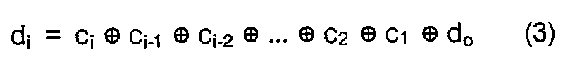
- d i c i ⁇ d i-1 (2)
- d i designates decoded data
- c i designates the received data before the decoding.
- Formula (2) represents that in order to obtain the i-th decoded data, one-bit previously decoded data [(i-1)th data] may be added to the i-th received data using 2 as modulus. So, the decoded data d is input to the one-bit delay circuit 7 and delayed by one bit, and then adding it to the received data c using 2 as modulus is performed in the EX-OR 8 thereby next decoded data d is obtained. This state is shown in c i , d i in FIG. 2.
- Second problem is in that since the data transmission path 5 includes noise, the received data c includes error, and after decoding this error propagates in the subsequent data through the sum conversion and so-called error propagation occurs.
- This state is shown in c i , d i of FIG. 2.
- error occurs in c11 and c17.
- the data d i after the decoding not only the error of c11 results in the error of one bit in d11, but the inversion of data continues subsequently and the error of the decoded data d i continues until the data is inverted again in the next received error bit c17 and returned to the original state.
- any of the decoded data is inverted and results in error until the next error of the received data occurs.
- an object of the present invention is to provide a sum decoding circuit wherein the error propagation due to the sum decoding is stopped at regular intervals, spread of the error is suppressed and the error rate characteristics can be improved.
- the invention provides data setting means using the known data as feedback data in matching with the receiving timing of the known data inserted in the data series.
- the known data is inserted in the data series before the transmission difference conversion and the created difference codes are received, and at the receiving timing of the known data, the known correct data is applied as the data after the decoding. Since the correct data is forcedly fed back as the data after the decoding as above described, the error propagation is stopped and the enlargement of the error is inhibited.
- FIG. 3 is a block diagram showing a sum decoding circuit as a first embodiment of the invention.
- numeral 6 designates an input terminal where received data c are input
- numeral 7 designates a one-bit delay circuit
- numeral 8 designates an EX-OR
- numeral 9 designates an output terminal where data d after the decoding are output
- numeral 10 designates a clock recovery circuit
- numeral 11 designates a frame recovery circuit
- numeral 12 designates a timing generator of receiving the known data
- numeral 13 designates a data selector.
- el designates output signal of the one-bit delay circuit 7 being one-bit previously decoded data
- e2 designates the initial value of the decoding (The initial value is 1 or "H” level in this case.)
- e3 designates the known data (the known data is 0 or "L” level in this case.).
- FIG. 4 is a diagram illustrating state that the error propagation is stopped by inserting the known data, where c i in FIG. 4(a) designates the received data, d i in FIG. 4(b) designates the data after the decoding, numerals 14a, 14b designate the frame synchronization bit series before the decoding and after the decoding respectively, numeral 15 designates the known data included in the data after the decoding, and numeral 16 designates the error portion of the data d i after the decoding. Also f in FIG. 4(c) designates the frame synchronization signal, and g in FIG. 4(d) designates the timing signal of receiving the known data.
- Signal transmitted by the transmitting side is one obtained by differentially coding the frame synchronization bit series and the effective data.
- the effective data the known data is inserted in the prescribed bit position.
- the clock signal h is regenerated from the input signal c in the clock recovery circuit 10.
- the clock recovery circuit 10 is constituted by PLL for example.
- the frame synchronization signal f is generated from the input signal c and the recovery clock signal h in the frame recovery circuit 11.
- the frame recovery circuit 11 for example, as shown in FIG. 5, is realized by a digital correlator comprising a shift register 111, a switch group 112, EX-OR 113, a parallel counter 114 and a digital comparator 115.
- the input data c is input to the shift register 111, and is shifted to the right direction one bit by one bit by the recovered clock signal h and stored.
- the switch group 112 is set to either "H" level or "L" level of each bit corresponding to the known frame synchronization signal before the decoding.
- the reference pattern by the switch group 112 and the received data are compared in parallel by the EX-OR 113, and a number of coincident data is output from the parallel counter 114 in binary notation.
- the digital comparator 115 compares the output data of the parallel counter 114 with the threshold data (constant value) previously set, and when the output data value of the parallel counter 114 exceeds the constant threshold value, the frame synchronization signal f is output.
- the frame synchronization signal f is input to the data selector 13 and the timing generator 12 for generating the timing of receiving the known data in FIG. 3. Since the position of the known data inserted into the generated data from the transmitting side, for example, a 128th bit of data succeeding the frame synchronization bit series, the timing generator 12 can be realized in the constitution shown in FIG. 6 for example.
- numeral 121 designates a counter
- numeral 122 designates a digital comparator.
- the counter 121 is reset by the frame synchronization signal f, and advances at each rise of the clock signal h. Consequently, the number of the counter 121 indicates the number of bits from the top end of the data.
- the digital comparator 122 compares the count value with the reference data representing the position of the known data previously set, and when both are coincident, the timing signal g of receiving the known data is output. The timing signal g of receiving the known data is input to the select input of the data selector 13.
- FIG. 4 shows the timing of the received data c, the frame synchronization signal f and the timing signal g of receiving the known data. Operation of the data selector 13 will be described referring to FIG. 4. At the usual data receiving state, both the frame synchronization signal f and the timing signal g of receiving the known data are at "L" level. Then the data selector 13 selects el among three inputs of data e1, e2, e3, thus the one-bit previously decoded data is input to the EX-OR 8. Consequently, the decoding is performed in similar manner to that in the decoding circuit in the prior art.
- the data selector 13 selects the data e2
- the data e2 corresponds to the initial value of the data decoding, and d0 shown in formula (3) is input to the decoding circuit then.
- the timing signal g of receiving the known data is at "H” (then the signal h is at “L")
- the data selector 13 selects the data e3.
- the data e3 is data equal to the known data, and is made “L” in the embodiment.
- FIG. 7 is a block diagram showing a decoding circuit as a second embodiment of the invention.
- the decoding circuit is constituted so that data generated by the transmitting side has the known data series including frame synchronisation bits (hereinafter referred to as "mid-amble") at the center portion as shown in FIG. 8.
- mid-amble frame synchronisation bits
- numeral 11a designates a frame recovery circuit
- numeral 12 designates a timing generator of the timing of receiving the known data
- numeral 13 designates a data selector
- numeral 21 designates a buffer circuit of data
- numeral 22 designates a high-speed clock generator for generating the high speed clock i
- numeral 23 designates a frequency divider.
- numerals 24a, 24b designate non-transmitting portion
- numeral 25a designates rising portion of the transmitting power
- numeral 25b designates falling portion of the transmitting power
- numerals 26a, 26b designate tail bits
- numerals 27a, 27b designate data carrying the information
- numeral 28 designates a mid-amble.
- the mid-amble 28 for the frame synchronization is arranged at the center portion of the received signal.
- the received signal c is sampled with the high speed clock i, and stored in the buffer circuit 21 temporarily.
- the buffer circuit 21 is realized by a shift register, for example.
- the frame recovery circuit 11a of FIG. 7 is driven by the clock i at higher speed than the bit rate, and detects the mid-amble from the received signal c. That is, the frame recovery circuit 11a may be constituted in similar manner to the frame recovery circuit 11 shown in FIG. 5, but the number of steps of the shift register is Also the number of switches in the switch group 112 is equal to the number of steps of the shift register in this case.
- the recovery clock signal h is created as follows. First, the frequency divider 23 is reset by the frame synchronization signal f. Consequently, the phase of the recovery clock signal h is coincident to the phase of received signal c with reference to the frame synchronization signal f. And then the frequency divider 23 performs the frequency dividing of the high speed clock signal at the frequency dividing ratio of
- the first bit of the received signal c is input to the EX-OR 8 when the frame synchronization signal f is output, thereby the subsequent operation can be explained in similar manner to the first embodiment.
- the tail bit is used as the initial data, and any one bit among the mid-amble 28 is used as the inserted known data.
- the known data after the frame synchronization signal f appears at one position, but it may appear at plural positions.
- An embodiment in this case is shown in FIG. 9.
- a decoding circuit shown in FIG. 9 is a circuit which can be used when the known data to be utilized for stopping the error propagation exists at seven positions at most.
- the output signal lines of the timing generator 12a are enlarged to three lines, and prescribed pattern is output at respective timings of the known data existing at seven positions at most.
- the data selector 13 selects either one among seven data previously set as the known data and the initial value or the ordinarily decoded data.
- the timing generator 12a may be constituted in similar manner to that shown in FIG. 6, but the digital comparator 122 is constituted to enable comparison of the comparing data of seven sorts at most with the output of the counter 121, and when each comparing data and the output of the counter 121 are coincident, pattern corresponding to each comparing data is output.
- FIG. 10 is a block diagram of a decoding circuit as a fourth embodiment of the invention where the feedback data is determined by a logical circuit 29 in place of by the set value and the data selector 13.
- the output signal of the logical circuit 29 is determined as shown in FIG. 11, and the decoding circuit performs operation in similar manner to the data selector 13 shown in FIG. 3 and the circuit using the set values e1 - e3.
Landscapes
- Engineering & Computer Science (AREA)
- Physics & Mathematics (AREA)
- Computer Networks & Wireless Communication (AREA)
- Signal Processing (AREA)
- Probability & Statistics with Applications (AREA)
- Theoretical Computer Science (AREA)
- Spectroscopy & Molecular Physics (AREA)
- Synchronisation In Digital Transmission Systems (AREA)
- Dc Digital Transmission (AREA)
- Detection And Prevention Of Errors In Transmission (AREA)
- Digital Transmission Methods That Use Modulated Carrier Waves (AREA)
- Bidirectional Digital Transmission (AREA)
Abstract
A decoding circuit in the invention receives signals encoded in differential logical conversion, and decodes it into an original signals. During the decoding, a bit position of known data included in the original signals in the received signal is detected, and also the known data is forcedly set to the bit position of the decoded signal, thereby spread of bit error is suppressed up to the position of the known data. <IMAGE>
Description
- The present invention relates to a decoding circuit where codes created by differential coding are decoded.
- FIG. 1 is a block diagram showing a decoding circuit where codes by the differential logical conversion are decoded (hereinafter referred to as "sum decoding circuit") together with a differential logical circuit at the transmitting side in the prior art. In FIG. 1,
numeral 1 designates an input terminal where digital data a are input,numeral 2 designates a one-bit delay circuit constituted by one D-type flip-flop for example,numeral 3 designates an exclusive-OR circuit (hereinafter referred to as "EX-OR") for creating the difference,numeral 4 designates an output terminal where transmitting data b are output,numeral 5 designates a transmission path having noise,numeral 6 designates an input terminal where received data c including error are input,numeral 7 designates a one-bit delay circuit,numeral 8 designates an EX-OR for creating the sum, andnumeral 9 designates an output terminal where data d after the sum decoding are output. - Next, operation will be described. The differential logical conversion at the transmitting side is expressed by following formula.

Where ai designates data before the conversion, and bi designates data after the conversion, and ai and bi correspond to a, b respectively in FIG. 1. Subscript i represents the i-th data. Also ⊕ represents the addition using 2 as modulus. The input data a is input to one of two input terminals of theEX-OR 3, and also input to the one-bit delay circuit 2. Consequently, viewing from the time series, the output signal of the one-bit delay circuit 2 is one-bit previous data ai-1. The EX-OR 3 performs the addition in the signal a, i.e., ai as one input and the output signal ai-1 of the one-bit delay circuit 2 as the other input using 2 as modulus, and obtains the output signal b, i.e., bi. FIG. 2 shows the relation between ai and bi, for example. - The decoding on the receiving side is expressed by following formula.

Where di designates decoded data, and ci designates the received data before the decoding. Formula (2) represents that in order to obtain the i-th decoded data, one-bit previously decoded data [(i-1)th data] may be added to the i-th received data using 2 as modulus. So, the decoded data d is input to the one-bit delay circuit 7 and delayed by one bit, and then adding it to the received data c using 2 as modulus is performed in theEX-OR 8 thereby next decoded data d is obtained. This state is shown in ci, di in FIG. 2. - In the sum conversion decoding at the receiving side, two problems occur as follows.
- One is a problem in the initial value.
Transforming the formula (2), it follows that
The decoded data di is determined by the received data series c₁ - ci and the initial value d₀ which cannot be determined only by the received data. The initial value d₀ is usually specified in the system thereby the problem is solved. - Second problem is in that since the
data transmission path 5 includes noise, the received data c includes error, and after decoding this error propagates in the subsequent data through the sum conversion and so-called error propagation occurs. This state is shown in ci, di of FIG. 2. In the received data ci, error occurs in c₁₁ and c₁₇. In the data di after the decoding, not only the error of c₁₁ results in the error of one bit in d₁₁, but the inversion of data continues subsequently and the error of the decoded data di continues until the data is inverted again in the next received error bit c₁₇ and returned to the original state. Thus, if error of one bit occurs in the received data, any of the decoded data is inverted and results in error until the next error of the received data occurs. - Since the sum decoding circuit in the prior art is constituted as described above, problems exist in that the error propagation is produced and the error is enlarged significantly in the decoding circuit.
- In view of the above-mentioned problems in the prior art, an object of the present invention is to provide a sum decoding circuit wherein the error propagation due to the sum decoding is stopped at regular intervals, spread of the error is suppressed and the error rate characteristics can be improved.
- In order to attain such object, the invention provides data setting means using the known data as feedback data in matching with the receiving timing of the known data inserted in the data series.
- In the decoding circuit according to the invention, the known data is inserted in the data series before the transmission difference conversion and the created difference codes are received, and at the receiving timing of the known data, the known correct data is applied as the data after the decoding. Since the correct data is forcedly fed back as the data after the decoding as above described, the error propagation is stopped and the enlargement of the error is inhibited.
-
- FIG. 1 is a block diagram showing a sum decoding circuit and a differential logical conversion circuit in the prior art;
- FIG. 2 is an explanation diagram illustrating an example of coding and decoding of differential codes;
- FIG. 3 is a block diagram showing a decoding circuit as a first embodiment of the invention;
- FIG. 4 is a timing chart illustrating operation of the decoding circuit shown in FIG. 3;
- FIG. 5 is a circuit diagram showing a frame recovery circuit;
- FIG. 6 is a circuit diagram showing a timing generator for generating the receiving timing of the known data;
- FIG. 7 is a block diagram showing a decoding circuit as a second embodiment of the invention;
- FIG. 8 is a data constitution diagram illustrating constitution of data having mid-amble;
- FIG. 9 is a block diagram showing a decoding circuit as a third embodiment of the invention;
- FIG. 10 is a block diagram showing a decoding circuit as a fourth embodiment of the invention; and
- FIG. 11 is a logic diagram illustrating operation of the logical circuit shown in FIG. 10.
- A sum decoding circuit as an embodiment of the invention will now be described referring to the accompanying drawings.
- FIG. 3 is a block diagram showing a sum decoding circuit as a first embodiment of the invention. In FIG. 3,
numeral 6 designates an input terminal where received data c are input,numeral 7 designates a one-bit delay circuit,numeral 8 designates an EX-OR,numeral 9 designates an output terminal where data d after the decoding are output,numeral 10 designates a clock recovery circuit,numeral 11 designates a frame recovery circuit,numeral 12 designates a timing generator of receiving the known data, andnumeral 13 designates a data selector. Also el designates output signal of the one-bit delay circuit 7 being one-bit previously decoded data, e2 designates the initial value of the decoding (The initial value is 1 or "H" level in this case.), and e3 designates the known data (the known data is 0 or "L" level in this case.). - FIG. 4 is a diagram illustrating state that the error propagation is stopped by inserting the known data, where ci in FIG. 4(a) designates the received data, di in FIG. 4(b) designates the data after the decoding,
numerals numeral 15 designates the known data included in the data after the decoding, andnumeral 16 designates the error portion of the data di after the decoding. Also f in FIG. 4(c) designates the frame synchronization signal, and g in FIG. 4(d) designates the timing signal of receiving the known data. - Next, operation will be described. Signal transmitted by the transmitting side is one obtained by differentially coding the frame synchronization bit series and the effective data. In the effective data, the known data is inserted in the prescribed bit position. In the decoding circuit, the clock signal h is regenerated from the input signal c in the
clock recovery circuit 10. In this case, theclock recovery circuit 10 is constituted by PLL for example. Also the frame synchronization signal f is generated from the input signal c and the recovery clock signal h in theframe recovery circuit 11. - The
frame recovery circuit 11, for example, as shown in FIG. 5, is realized by a digital correlator comprising ashift register 111, aswitch group 112, EX-OR 113, aparallel counter 114 and adigital comparator 115. First, the input data c is input to theshift register 111, and is shifted to the right direction one bit by one bit by the recovered clock signal h and stored. Theswitch group 112 is set to either "H" level or "L" level of each bit corresponding to the known frame synchronization signal before the decoding. The reference pattern by theswitch group 112 and the received data are compared in parallel by theEX-OR 113, and a number of coincident data is output from theparallel counter 114 in binary notation. Thedigital comparator 115 compares the output data of theparallel counter 114 with the threshold data (constant value) previously set, and when the output data value of theparallel counter 114 exceeds the constant threshold value, the frame synchronization signal f is output. - The frame synchronization signal f is input to the
data selector 13 and thetiming generator 12 for generating the timing of receiving the known data in FIG. 3. Since the position of the known data inserted into the generated data from the transmitting side, for example, a 128th bit of data succeeding the frame synchronization bit series, thetiming generator 12 can be realized in the constitution shown in FIG. 6 for example. - In FIG. 6, numeral 121 designates a counter, and numeral 122 designates a digital comparator. The
counter 121 is reset by the frame synchronization signal f, and advances at each rise of the clock signal h. Consequently, the number of thecounter 121 indicates the number of bits from the top end of the data. Thedigital comparator 122 compares the count value with the reference data representing the position of the known data previously set, and when both are coincident, the timing signal g of receiving the known data is output. The timing signal g of receiving the known data is input to the select input of thedata selector 13. - FIG. 4 shows the timing of the received data c, the frame synchronization signal f and the timing signal g of receiving the known data. Operation of the
data selector 13 will be described referring to FIG. 4. At the usual data receiving state, both the frame synchronization signal f and the timing signal g of receiving the known data are at "L" level. Then thedata selector 13 selects el among three inputs of data e1, e2, e3, thus the one-bit previously decoded data is input to theEX-OR 8. Consequently, the decoding is performed in similar manner to that in the decoding circuit in the prior art. When the frame synchronization signal f is at "H" (then the timing signal g of receiving the known data is at "L"), thedata selector 13 selects the data e2 The data e2 corresponds to the initial value of the data decoding, and d₀ shown in formula (3) is input to the decoding circuit then. When the timing signal g of receiving the known data is at "H" (then the signal h is at "L"), thedata selector 13 selects the data e3. The data e3 is data equal to the known data, and is made "L" in the embodiment. Consequently, in the timing of receiving the known data, the feedback loop of the decoding circuit is cut, and the correct decoded data is supplied to the decoding circuit irrespectively of whether the one-bit previously decoded data is correct or not. Consequently, the error propagation is stopped at the timing of receiving the known data. In FIG. 4, "x" at (a) indicates the occurrence of the data error, and numeral 16 indicates the error portion of the data after the decoding. - FIG. 7 is a block diagram showing a decoding circuit as a second embodiment of the invention. The decoding circuit is constituted so that data generated by the transmitting side has the known data series including frame synchronisation bits (hereinafter referred to as "mid-amble") at the center portion as shown in FIG. 8.
- In FIG. 7, numeral 11a designates a frame recovery circuit, numeral 12 designates a timing generator of the timing of receiving the known data, numeral 13 designates a data selector, numeral 21 designates a buffer circuit of data, numeral 22 designates a high-speed clock generator for generating the high speed clock i, and numeral 23 designates a frequency divider. Also in FIG. 8, numerals 24a, 24b designate non-transmitting portion, numeral 25a designates rising portion of the transmitting power, numeral 25b designates falling portion of the transmitting power,
numerals 26a, 26b designate tail bits,numerals 27a, 27b designate data carrying the information, and numeral 28 designates a mid-amble. - Operation of the second embodiment will be described. As shown in FIG. 8, the mid-amble 28 for the frame synchronization is arranged at the center portion of the received signal. The received signal c is sampled with the high speed clock i, and stored in the
buffer circuit 21 temporarily. In this case, thebuffer circuit 21 is realized by a shift register, for example. The frame recovery circuit 11a of FIG. 7 is driven by the clock i at higher speed than the bit rate, and detects the mid-amble from the received signal c. That is, the frame recovery circuit 11a may be constituted in similar manner to theframe recovery circuit 11 shown in FIG. 5, but the number of steps of the shift register is
Also the number of switches in theswitch group 112 is equal to the number of steps of the shift register in this case. - Also the recovery clock signal h is created as follows. First, the
frequency divider 23 is reset by the frame synchronization signal f. Consequently, the phase of the recovery clock signal h is coincident to the phase of received signal c with reference to the frame synchronization signal f. And then thefrequency divider 23 performs the frequency dividing of the high speed clock signal at the frequency dividing ratio of
- If the number of steps of the
buffer circuit 21 being the shift register is set so that the data received before the frame synchronization signal is stored in thebuffer circuit 21, the first bit of the received signal c is input to theEX-OR 8 when the frame synchronization signal f is output, thereby the subsequent operation can be explained in similar manner to the first embodiment. However, the tail bit is used as the initial data, and any one bit among the mid-amble 28 is used as the inserted known data. - In the embodiment shown in FIG. 3, the known data after the frame synchronization signal f appears at one position, but it may appear at plural positions. An embodiment in this case is shown in FIG. 9. A decoding circuit shown in FIG. 9 is a circuit which can be used when the known data to be utilized for stopping the error propagation exists at seven positions at most. In this case, the output signal lines of the
timing generator 12a are enlarged to three lines, and prescribed pattern is output at respective timings of the known data existing at seven positions at most. Corresponding to this pattern, thedata selector 13 selects either one among seven data previously set as the known data and the initial value or the ordinarily decoded data. - The
timing generator 12a may be constituted in similar manner to that shown in FIG. 6, but thedigital comparator 122 is constituted to enable comparison of the comparing data of seven sorts at most with the output of thecounter 121, and when each comparing data and the output of thecounter 121 are coincident, pattern corresponding to each comparing data is output. - FIG. 10 is a block diagram of a decoding circuit as a fourth embodiment of the invention where the feedback data is determined by a
logical circuit 29 in place of by the set value and thedata selector 13. The output signal of thelogical circuit 29 is determined as shown in FIG. 11, and the decoding circuit performs operation in similar manner to thedata selector 13 shown in FIG. 3 and the circuit using the set values e1 - e3.
Claims (9)
- A decoding circuit for inhibiting error propagation, wherein a signal having a frame synchronization bit series, inserted known data therein and subjected to differential logical conversion is received, and decoded into an original signal by performing exclusive-OR operation between a presently decoded bit of the received signal and a previously decoded bit decoded immediately before the presently decoded bit, said decoding circuit comprising:
known data timing determining means for determining a bit position of the known data in the received signal; and
data setting means for forcedly setting data equal to the known data to the bit position in the received signal determined by said known data timing determining means. - A decoding circuit for inhibiting error propagation as set forth in claim 1, wherein said known data timing determining means comprises: a clock recovery circuit for regenerating a synchronized clock signal from the received signal; a frame recovery circuit for comparing the received signal sampled by the clock signal with a reference pattern being equal to the frame synchronization bit series, and for outputting the frame synchronization signal when both are coincident; and a timing generator for counting the recovered clock signal since when the frame synchronization signal is output, and for outputting a timing signal indicating the bit position of the known data in the received signal.
- A decoding circuit for inhibiting error propagation as set forth in claim 2, wherein said data setting means is a data selector which selects an initial value of decoding operation based on the frame synchronization signal, selects data equal to the known data based on the output of said timing generator and selects the previously decoded bit in other cases.
- A decoding circuit for inhibiting error propagation as set forth in claim 3, wherein said timing generator comprises: a counter for counting the clock signals; and a comparator for comparing an output value of said counter with reference data indicating the number of bits from a bit corresponding to the frame synchronization signal to a bit where the known data exists, and for generating the timing signal when both are coincident.
- A decoding circuit for inhibiting error propagation as set forth in claim 4, wherein said comparator has a plurality of the reference data and outputs the plurality of the timing signals during receiving one frame, and said data selector outputs data equal to one among the plurality of known data corresponding to the plurality of timing signals respectively.
- A decoding circuit for inhibiting error propagation, wherein a signal having a known data series including a frame synchronization bit series therein and subjected to differential logical conversion is received, and decoded into an original signal by performing exclusive-OR operation between a presently decoded bit of the received signal and a previously decoded bit decoded immediately before the presently decoded bit, said decoding circuit comprising:
a buffer circuit for storing the received signal temporarily;
a synchronization detecting circuit for detecting the frame synchronization bit series and the known data series from the received signal, and for outputting a frame synchronization signal a timing signal indicating a bit position of the known data; and
data setting means for forcedly setting a value of the known data to the bit position indicated by the timing signal among the received signals output from said buffer circuit in synchronism with the frame synchronization signal. - A decoding circuit for inhibiting error propagation as set forth in claim 6, wherein said synchronization detecting circuit comprises: a high speed clock generator for generating a high speed clock signal at a higher speed than a bit rate of the received signal; a frame recovery circuit for comparing the received signal sampled by the high speed clock signal with a reference pattern being equal to the frame synchronization bit series, and for outputting the frame synchronization signal; and a timing generator for generating said timing signal based on both the high speed clock signal from the high speed clock generator and the frame synchronization signal from the frame recovery circuit.
- A decoding circuit for inhibiting error propagation as set forth in claim 7, wherein said data setting means is a data selector which selects an initial value of detecting operation based on the frame synchronization signal, selects data equal to the known data based on the output of said timing generator and selects the previously decoded bit in other cases.
- A decoding circuit for inhibiting error propagation as set forth in claim 8, wherein said buffer circuit is a shift register, a number of stages of which is equal to that of bits generated by sampling the received data with the high speed clock signal until generation of the frame synchronization signal.
Applications Claiming Priority (2)
| Application Number | Priority Date | Filing Date | Title |
|---|---|---|---|
| JP2092638A JPH03291033A (en) | 1990-04-06 | 1990-04-06 | Sum decoding circuit |
| JP92638/90 | 1990-04-06 |
Publications (2)
| Publication Number | Publication Date |
|---|---|
| EP0450148A2 true EP0450148A2 (en) | 1991-10-09 |
| EP0450148A3 EP0450148A3 (en) | 1992-03-11 |
Family
ID=14059992
Family Applications (1)
| Application Number | Title | Priority Date | Filing Date |
|---|---|---|---|
| EP19900120169 Withdrawn EP0450148A3 (en) | 1990-04-06 | 1990-10-20 | Decoding circuit for inhibiting error propagation |
Country Status (4)
| Country | Link |
|---|---|
| US (1) | US5265105A (en) |
| EP (1) | EP0450148A3 (en) |
| JP (1) | JPH03291033A (en) |
| NO (1) | NO904270L (en) |
Families Citing this family (6)
| Publication number | Priority date | Publication date | Assignee | Title |
|---|---|---|---|---|
| FR2798540B1 (en) * | 1999-09-13 | 2001-11-23 | France Telecom | METHOD OF JOINT DECODING AND EQUALIZATION OF A DIGITAL SIGNAL PROTECTED BY A CODE DEFINED BY A MESH |
| DE60016592T2 (en) * | 2000-09-20 | 2005-12-22 | Lucent Technologies Inc. | Radio system, antenna arrangement and polarization modulator for generating a transmission signal with variable polarization |
| US8126089B2 (en) * | 2004-09-30 | 2012-02-28 | Alcatel Lucent | Method and apparatus for providing frame synchronization in a digital communication system that supports multiple modulation formats |
| US7616724B2 (en) * | 2004-09-30 | 2009-11-10 | Alcatel-Lucent Usa Inc. | Method and apparatus for multi-modulation frame synchronization in a digital communication system |
| WO2011059419A1 (en) * | 2009-11-13 | 2011-05-19 | Thomson Licensing | Preamble identification in a mobile dtv system |
| US9391741B2 (en) * | 2009-11-13 | 2016-07-12 | Thomson Licensing | Joint preamble and code rate identifier in a mobile DTV system |
Family Cites Families (10)
| Publication number | Priority date | Publication date | Assignee | Title |
|---|---|---|---|---|
| US4530094A (en) * | 1982-09-28 | 1985-07-16 | Ael Microtel, Limited | Coding for odd error multiplication in digital systems with differential coding |
| JPS5975741A (en) * | 1982-10-22 | 1984-04-28 | Akai Electric Co Ltd | Mfm modulating and demodulating circuit |
| JPH0697756B2 (en) * | 1985-01-28 | 1994-11-30 | 日本電信電話株式会社 | Pulse multiplex communication system |
| JPH06105891B2 (en) * | 1985-03-19 | 1994-12-21 | キヤノン株式会社 | Data transmission method |
| JPS62141875A (en) * | 1985-12-16 | 1987-06-25 | Fujitsu Ltd | Preventing system for propagation of decoding error |
| JPS62281531A (en) * | 1986-05-29 | 1987-12-07 | Nec Corp | Difference pulse coding system |
| JPH01296840A (en) * | 1988-05-25 | 1989-11-30 | Fujitsu Ltd | Error correcting system for signal |
| GB2226206B (en) * | 1988-12-14 | 1993-03-17 | Stc Plc | Hybrid pcm/dpcm codec |
| US5130993A (en) * | 1989-12-29 | 1992-07-14 | Codex Corporation | Transmitting encoded data on unreliable networks |
| JPH03270526A (en) * | 1990-03-20 | 1991-12-02 | Fujitsu Ltd | Error inflection suppressing system in differential encoding |
-
1990
- 1990-04-06 JP JP2092638A patent/JPH03291033A/en active Pending
- 1990-09-28 US US07/590,190 patent/US5265105A/en not_active Expired - Fee Related
- 1990-10-01 NO NO90904270A patent/NO904270L/en not_active Application Discontinuation
- 1990-10-20 EP EP19900120169 patent/EP0450148A3/en not_active Withdrawn
Also Published As
| Publication number | Publication date |
|---|---|
| NO904270L (en) | 1991-10-07 |
| JPH03291033A (en) | 1991-12-20 |
| NO904270D0 (en) | 1990-10-01 |
| EP0450148A3 (en) | 1992-03-11 |
| US5265105A (en) | 1993-11-23 |
Similar Documents
| Publication | Publication Date | Title |
|---|---|---|
| US4506372A (en) | Method and apparatus for recognizing in a receiver the start of a telegram signal consisting of a bit impulse sequence | |
| JP3671920B2 (en) | Skew adjustment circuit and skew adjustment method | |
| US4667327A (en) | Error corrector for a linear feedback shift register sequence | |
| US5717728A (en) | Data/clock recovery circuit | |
| EP0450148A2 (en) | Decoding circuit for inhibiting error propagation | |
| US6977973B1 (en) | System and method for decoding manchester data | |
| US4740998A (en) | Clock recovery circuit and method | |
| KR100287268B1 (en) | Pattern matching equipment | |
| US6192093B1 (en) | Enhanced CIMT coding system and method with automatic word alignment for simplex operation | |
| JP2947074B2 (en) | Frame synchronization detection circuit | |
| US4606056A (en) | Method of encoding and serially transmitting self-clocking data and control characters | |
| CA2038472C (en) | System for suppressing spread of error generated in differential coding | |
| US5636248A (en) | Method and system for regenerating amplitude and timing characteristics of an analog signal | |
| US5430733A (en) | Digital transmission system for multiplexing and demultiplexing signals | |
| US4498167A (en) | TDM Communication system | |
| JP3465386B2 (en) | Frame synchronization circuit and encoding / decoding processing circuit using the same | |
| KR100300947B1 (en) | Method and device for excluding error packet in data communication system | |
| US4437086A (en) | Limited look-ahead means | |
| RU2206181C1 (en) | Data coding/decoding device | |
| US6970527B2 (en) | Transmitting circuit and method thereof, receiving circuit and method thereof, and data communication apparatus | |
| JP3478290B2 (en) | DUTY correction circuit | |
| JP2668968B2 (en) | Frame synchronization method | |
| SU815946A1 (en) | Device for cycle-wise synchronization | |
| JPS60235549A (en) | C-bit synchronism system of nb1c code signal | |
| JP3458782B2 (en) | DUTY correction circuit |
Legal Events
| Date | Code | Title | Description |
|---|---|---|---|
| PUAI | Public reference made under article 153(3) epc to a published international application that has entered the european phase |
Free format text: ORIGINAL CODE: 0009012 |
|
| AK | Designated contracting states |
Kind code of ref document: A2 Designated state(s): FR GB SE |
|
| PUAL | Search report despatched |
Free format text: ORIGINAL CODE: 0009013 |
|
| AK | Designated contracting states |
Kind code of ref document: A3 Designated state(s): FR GB SE |
|
| 17P | Request for examination filed |
Effective date: 19920409 |
|
| 18W | Application withdrawn |
Withdrawal date: 19921211 |
|
| STAA | Information on the status of an ep patent application or granted ep patent |
Free format text: STATUS: THE APPLICATION HAS BEEN WITHDRAWN |
|
| R18W | Application withdrawn (corrected) |
Effective date: 19921211 |