EP0450223B1 - Cadre conducteur pour empaquetage d'un semi-conducteur par résine - Google Patents
Cadre conducteur pour empaquetage d'un semi-conducteur par résine Download PDFInfo
- Publication number
- EP0450223B1 EP0450223B1 EP90309862A EP90309862A EP0450223B1 EP 0450223 B1 EP0450223 B1 EP 0450223B1 EP 90309862 A EP90309862 A EP 90309862A EP 90309862 A EP90309862 A EP 90309862A EP 0450223 B1 EP0450223 B1 EP 0450223B1
- Authority
- EP
- European Patent Office
- Prior art keywords
- lead frame
- chip
- thermal expansion
- metal foil
- copper
- Prior art date
- Legal status (The legal status is an assumption and is not a legal conclusion. Google has not performed a legal analysis and makes no representation as to the accuracy of the status listed.)
- Expired - Lifetime
Links
Images


Classifications
-
- H—ELECTRICITY
- H10—SEMICONDUCTOR DEVICES; ELECTRIC SOLID-STATE DEVICES NOT OTHERWISE PROVIDED FOR
- H10W—GENERIC PACKAGES, INTERCONNECTIONS, CONNECTORS OR OTHER CONSTRUCTIONAL DETAILS OF DEVICES COVERED BY CLASS H10
- H10W70/00—Package substrates; Interposers; Redistribution layers [RDL]
- H10W70/40—Leadframes
- H10W70/456—Materials
- H10W70/457—Materials of metallic layers on leadframes
-
- H—ELECTRICITY
- H10—SEMICONDUCTOR DEVICES; ELECTRIC SOLID-STATE DEVICES NOT OTHERWISE PROVIDED FOR
- H10W—GENERIC PACKAGES, INTERCONNECTIONS, CONNECTORS OR OTHER CONSTRUCTIONAL DETAILS OF DEVICES COVERED BY CLASS H10
- H10W70/00—Package substrates; Interposers; Redistribution layers [RDL]
- H10W70/40—Leadframes
- H10W70/421—Shapes or dispositions
- H10W70/424—Cross-sectional shapes
-
- H—ELECTRICITY
- H10—SEMICONDUCTOR DEVICES; ELECTRIC SOLID-STATE DEVICES NOT OTHERWISE PROVIDED FOR
- H10W—GENERIC PACKAGES, INTERCONNECTIONS, CONNECTORS OR OTHER CONSTRUCTIONAL DETAILS OF DEVICES COVERED BY CLASS H10
- H10W90/00—Package configurations
- H10W90/811—Multiple chips on leadframes
-
- H—ELECTRICITY
- H10—SEMICONDUCTOR DEVICES; ELECTRIC SOLID-STATE DEVICES NOT OTHERWISE PROVIDED FOR
- H10W—GENERIC PACKAGES, INTERCONNECTIONS, CONNECTORS OR OTHER CONSTRUCTIONAL DETAILS OF DEVICES COVERED BY CLASS H10
- H10W72/00—Interconnections or connectors in packages
- H10W72/50—Bond wires
- H10W72/531—Shapes of wire connectors
- H10W72/536—Shapes of wire connectors the connected ends being ball-shaped
-
- H—ELECTRICITY
- H10—SEMICONDUCTOR DEVICES; ELECTRIC SOLID-STATE DEVICES NOT OTHERWISE PROVIDED FOR
- H10W—GENERIC PACKAGES, INTERCONNECTIONS, CONNECTORS OR OTHER CONSTRUCTIONAL DETAILS OF DEVICES COVERED BY CLASS H10
- H10W72/00—Interconnections or connectors in packages
- H10W72/50—Bond wires
- H10W72/531—Shapes of wire connectors
- H10W72/5363—Shapes of wire connectors the connected ends being wedge-shaped
-
- H—ELECTRICITY
- H10—SEMICONDUCTOR DEVICES; ELECTRIC SOLID-STATE DEVICES NOT OTHERWISE PROVIDED FOR
- H10W—GENERIC PACKAGES, INTERCONNECTIONS, CONNECTORS OR OTHER CONSTRUCTIONAL DETAILS OF DEVICES COVERED BY CLASS H10
- H10W72/00—Interconnections or connectors in packages
- H10W72/50—Bond wires
- H10W72/551—Materials of bond wires
- H10W72/552—Materials of bond wires comprising metals or metalloids, e.g. silver
- H10W72/5525—Materials of bond wires comprising metals or metalloids, e.g. silver comprising copper [Cu]
-
- H—ELECTRICITY
- H10—SEMICONDUCTOR DEVICES; ELECTRIC SOLID-STATE DEVICES NOT OTHERWISE PROVIDED FOR
- H10W—GENERIC PACKAGES, INTERCONNECTIONS, CONNECTORS OR OTHER CONSTRUCTIONAL DETAILS OF DEVICES COVERED BY CLASS H10
- H10W72/00—Interconnections or connectors in packages
- H10W72/851—Dispositions of multiple connectors or interconnections
- H10W72/874—On different surfaces
- H10W72/884—Die-attach connectors and bond wires
-
- H—ELECTRICITY
- H10—SEMICONDUCTOR DEVICES; ELECTRIC SOLID-STATE DEVICES NOT OTHERWISE PROVIDED FOR
- H10W—GENERIC PACKAGES, INTERCONNECTIONS, CONNECTORS OR OTHER CONSTRUCTIONAL DETAILS OF DEVICES COVERED BY CLASS H10
- H10W74/00—Encapsulations, e.g. protective coatings
-
- H—ELECTRICITY
- H10—SEMICONDUCTOR DEVICES; ELECTRIC SOLID-STATE DEVICES NOT OTHERWISE PROVIDED FOR
- H10W—GENERIC PACKAGES, INTERCONNECTIONS, CONNECTORS OR OTHER CONSTRUCTIONAL DETAILS OF DEVICES COVERED BY CLASS H10
- H10W90/00—Package configurations
- H10W90/701—Package configurations characterised by the relative positions of pads or connectors relative to package parts
- H10W90/731—Package configurations characterised by the relative positions of pads or connectors relative to package parts of die-attach connectors
- H10W90/736—Package configurations characterised by the relative positions of pads or connectors relative to package parts of die-attach connectors between a chip and a stacked lead frame, conducting package substrate or heat sink
-
- H—ELECTRICITY
- H10—SEMICONDUCTOR DEVICES; ELECTRIC SOLID-STATE DEVICES NOT OTHERWISE PROVIDED FOR
- H10W—GENERIC PACKAGES, INTERCONNECTIONS, CONNECTORS OR OTHER CONSTRUCTIONAL DETAILS OF DEVICES COVERED BY CLASS H10
- H10W90/00—Package configurations
- H10W90/701—Package configurations characterised by the relative positions of pads or connectors relative to package parts
- H10W90/751—Package configurations characterised by the relative positions of pads or connectors relative to package parts of bond wires
- H10W90/756—Package configurations characterised by the relative positions of pads or connectors relative to package parts of bond wires between a chip and a stacked lead frame, conducting package substrate or heat sink
Definitions
- the present invention concerns resin-sealed semiconductor packages in combination with Cu based lead frames.
- the lead frames for semiconductor packages made of synthetic resin material have generally been made of copper alloys with good thermal conductivity, in view of the heat dissipation capacity requirement.
- copper alloys are not so favourable since they do not match the thermal expansion coefficient of the chips, and there is therefore a danger of peeling at the bonding interface between the chip and the lead frame island or cracking of the chip.
- Integrated circuit chips (hereinafter referred to as "chips") of semiconductor packages, and especially LSI or VLSI chips for large-scale computers, are attaining a high degree of integration and increased operation speed.
- the quantity of heat generated by the operation of the devices has thus become extremely large, because of the large amount of the electric power consumed by their operation.
- the thermal expansion coefficient of the substrate material is significantly different from that of the material of the chip (made of silicon or gallium arsenic), there is a problem that the chip would suffer from peeling or cracking away from the substrate.
- the chip-carrying substrate must have a high heat dissipation capacity and thus a large thermal conductivity is required for the substrate material.
- the main object of the present invention is to provide a lead frame which has a high heat conductivity but is subject to little or no peeling or cracking from a chip attached thereto and encapsulated in resin.
- the present invention provides a combination of a resin-sealed semiconductor package and a lead frame comprising a semiconductor chip mounted on the lead frame and resin-sealed thereon within said package, said lead frame being made of a strip of copper or copper alloy sheet and said chip being mounted on an island portion of said lead frame, said island portion having bonded only on the side of the island portion opposite to where the said chip is mounted, a metal foil with a thermal expansion coefficient that is low with respect to that of copper or said copper alloy.
- the present invention results from various studies which the inventors have made of the bending of island portions during heating with chips mounted thereon.
- the purpose of these studies has been to improve the thermal bondability between a copper or copper alloy sheet of excellent heat dissipation and a chip of large capacity. It has been found that the warping, etc., during heating, of the side of the substrate on which the chip is mounted can be reduced, preventing damage to the chip such as peeling or cracking, by cladding metal foils of low thermal expansion in a spot-like pattern to the alloy sheet opposite where the semi-conductor chips are to be mounted.
- lead frame material made of a strip of copper or copper alloy sheet for use in resin packages, in which semiconductor chips are mounted and resin-sealed on island portions of lead frames fabricated from a strip of substrate material by means of punching, etc, wherein the lead frame material comprises a spot-clad material in which metal foils of low thermal expansion are roll-bonded and arranged along the substrate at positions to be formed into island portions, on the side opposite where semiconductor chips are to be mounted.
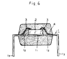
- Figure 6 shows a known form of resin-sealed semiconductor package.
- a lead frame not only serves as a path for electrically connecting a chip to the outside but also has an important role as a path for releasing the heat generated from the chip.
- a chip 2 is mounted on an island 11 formed by the central portion of a lead frame 1 and is fixed thereon with brazing material, adhesive, or solder.
- the chip 2 is also electrically connected with an inner lead 12 by way of a bonding wire 3 and the assembly is sealed by means of a resin encapsulation 4.
- the heat generated by the chip 2 reaches an outer lead 13 of the lead frame 1 by way of a path including the island 11, the resin 4, and the inner lead 12, and is then released to the outside through the outer surface of the resin 4.
- the lead frame 1 is desirable for the lead frame 1 to be made of a material having a high thermal conductivity, so that heat generated by the chip can be efficiently released to the outside of the semiconductor package.
- the lead frame material comprises a spot-clad material, in which metal foils 11 of low thermal expansion each of a predetermined size are bonded and arranged at predetermined intervals on the required side of a strip of Cu series substrate material 10 made of copper or copper alloy.
- the strip of Cu series substrate material 10 is shaped by punching into a plurality of lead frames of desired pattern.
- the metal foils 11 of low thermal expansion, each of a predetermined size, are roll-bonded and arranged at predetermined intervals along the length of the strip 10, forming island portions on the side opposite that on which the semiconductor chips are to be mounted.
- each of the metal foils 11 of low thermal expansion has its thickness and size selected with reference to the thickness of the Cu series substrate material 10, the size of the chip to be mounted, etc.
- the metal foils 11 of low thermal expansion may be roll-bonded to the surface of the Cu series substrate material 10 or partially or entirely embedded into the substrate material, as shown in Figures 2a, b and c.
- the metal foil 11 of low thermal expansion may be a punched metal sheet formed with a variety of shapes of apertures.
- the effective thermal expansion coefficient will lie between the copper or copper alloy and the metal material of low heat expansion in accordance with the volume ratio between the copper or copper alloy and the metal material of low thermal expansion.
- Cu series substrate material 10 there can be used, in addition to pure Cu, any of known Cu alloys such as Cu-Sn, Cu-Fe, Cu-Zn, Cu-Co, Cu-Ni, Cu-Zr or Cu series alloys further including P, Cr, etc, which can be selected depending on the application, required performance, etc.
- any of known Cu alloys such as Cu-Sn, Cu-Fe, Cu-Zn, Cu-Co, Cu-Ni, Cu-Zr or Cu series alloys further including P, Cr, etc, which can be selected depending on the application, required performance, etc.
- Ni-Fe series alloys of various compositions such as 36Ni-Fe alloy, 3- Ni-4Co-Fe alloy, 42 Ni-Fe alloy, any of known metal materials of low thermal expansion such as so-called Kovar alloy, Mo, Fe-Cr alloy, etc.
- FIG. 2a, b and c Various kinds of lead frame constructions as shown in Figures 2a, b and c may be used.
- a plurality of lead frames of desired pattern are shaped in the longitudinal direction, by for example punching, and resin packages are prepared from the resultant lead frames.
- a chip 2 is placed on an island 11 formed at the central portion of lead frame 1 as shown in Figures 4a, b and c.
- the chip 2 is fixed by means of brazing material, adhesive or solder, electrically connected with an inner lead 12 by means of a bonding wire 3, and then sealed therearound with a resin 4.
- a metal foil 11 of low thermal expansion is roll-bonded to an island 11 on the side opposite to that where a chip 2 is to be mounted.
- a metal foil 11 of low thermal expansion is entirely embedded in the surface of an island 11 to be the same thickness as other portions of the lead.
- a metal foil 11 of low thermal expansion constituted as a punched metal sheet is embedded in the surface of an island 11.
- heat generated by the chip 2 passes by way of the path including the island 11, the resin 4 and the inner lead 12 to the lead 13 of the lead frame 1 and is then released to the outside. Since the entire path is made of the Cu series substrate material, the heat dissipation capacity is extremely good.
- the metal foil 11 of a required low thermal expansion is roll-bonded and embedded on or in the surface of the island 11 opposite the chip 2, the lead frame undergoes almost no warping upon heating. Peeling, etc, at the bonding interface between the chip 2 and the island 11 is thus prevented, giving a highly reliable resin package.
- the lead frame of the invention comprises a spot-clad material in which metal foils 11 of low thermal expansion are placed against a strip of Cu series substrate material 10 made of copper or copper alloy, and are roll-bonded and rolled to predetermined intervals.
- the material, thickness, and size of the metal foil 11 are selected having regard to the thickness of the Cu series substrate 10 and the size of the chip to be mounted.
- the specific thickness and size of the metal foil 11 of low thermal expansion are selected mainly by confirming them in an actual mounting test.
- the island portion of the lead frame on which the chip is to be mounted is treated as a composite material comprising the chip, and the lead frame (substrate + metal foils of low thermal expansion) parameters and conditions for not bending the composite material are determined. That is, conditions are determined such that the amounts of bending upon heating through a temperature rise ⁇ T are equal and opposite for the low thermal expansion materials on the two surfaces of the substrate. Since the amount of bending is proportional to the bending coefficient in the case of the composition material, the conditions in which the bending coefficients become identical can be determined.
- the optimum thickness of the metal foils of low thermal expansion may be determined, depending on the chip to be mounted and the thickness of the Cu series substrate, by considering the relationship between the bending coefficients for the combinations of chip with substrate and substrate with metal foil of low thermal expansion, and the plate thickness ratio.
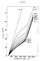
- curve (1) shows the bending coefficient of a silicon chip (thermal expansion coefficient: 4 x 10 ⁇ 6) with the Cu series substrate
- curve (2) shows the bending coefficient of Cu series substrate + 36Ni-Fe
- curves (3), (4) show the bending coefficients for Cu series substrate + Kovar (thermal expansion coefficient: 7-8x10 ⁇ 6).
- the thickness of the 36 Ni-Fe material is preferably 0.34 mm or 0.04 mm and the thickness of Kovar is preferably about 0.1 mm.
- metal foils of low thermal expansion of material, thickness and size are selected in the light of the kind and the thickness of the Cu series substrate, the size of the chip to be mounted, etc. These foils are stacked on the Cu series substrate, roll-bonded, and rolled till the desired thickness ratio is obtained.
- the metal foil of low thermal expansion is clad in a spot-like pattern along the longitudinal direction of the Cu series substrate material; its pitch and size should be of high accuracy when it is fabricated into a lead frame.
- a spot-clad material having pitch and size of high accuracy can be obtained, for example, by the following procedure: (1) uncoiling and intermittently feeding a metal foil and a Cu series substrate material, each by a predetermined length; (2) applying continuous supersonic welding to the foil and substrate at predetermined intervals; (3) cutting the metal foil at predetermined intervals by a pair of rotary cutters thereby removing loose metal foil pieces; (4) seizing and cutting a metal foil which is intermittently fed by predetermined lengths by means of a punching tool and, simultaneously, spot welding them on a Cu series substrate material which is also fed intermittently at predetermined lengths using an electrode incorporated in the punching tool, or by provisionally fixing them by supersonic welding using a supersonic welding vibration plate incorporated in a punching tool; and (5) then roll-bonding and rolling them.
- the spot-clad material can also be obtained by: (1) provisionally fixing a metal foil and a Cu series substrate material, which are each fed intermittently by predetermined lengths by means of laser welding continuously at predetermined intervals; (2) removing metal foil pieces which are not so fixed by cutting the metal foil at predetermined intervals by means of a rotary cutter or by seizing and cutting the metal foil intermittently fed by predetermined lengths and then provisionally fixing it on the Cu series substrate material which is also fed intermittently by predetermined lengths by means of laser welding while held by means of the punching tool and then (3) roll-bonding and rolling them.
- a high accuracy of pitch control can be attained by abutting backup rolls to a pair of work rolls of a rolling mill and providing a device for detecting the load upon pressurizing the uncoiled Cu series substrate material and a plate thickness gauge, and applying a constant load control by a rolling load controller.
- a quantitative relationship can be determined between the variations of the rolling load, the variations of the pitch, and the absolute position, based on the the measured value for the absolute position of the metal foil from a required original point and a control model and by calculating a target rolling load (refer to Japanese Patent Applications Hei 1-216759 and Hei 1-216760).
- the metal foil pieces can also be embedded into and arranged on the Cu series substrate material by means of a compression machine.
- the metal foil 11 of low thermal expansion is bonded to the Cu series substrate material 10 by means of pin-down bonding, a similar effect for preventing bending can also be obtained. Further, in a case where the metal foil 11 of low thermal expansion is embedded in the surface of the Cu series substrate material 10 on the side reverse to the area to be formed with an island as shown in Figure 2b, the bending preventive effect can similarly be obtained by merely attaching the metal foil 11 only at its ends or edges.
- Ag or Au can be plated in a strip or spot-like pattern at predetermined positions on the surface of the lead frame material on the side on which the chips are mounted; that is, the surface including the bonding area of the lead frame.
- foils of Ag, Au, Al, Cu, etc can be roll-bonded and rolled in a strip, of pattern depending on the kind of the bonding wire, at predetermined positions on the lead frame material on the side to have chips mounted on it.
- the method may be adopted of applying roll-bonding and rolling after cutting the foils into foil pieces and then provisionally fixing them.
- Cu wires can be used for the bonding.
- the bonding operation can be applied easily and reliably in the assembly step for the Cu alloy lead frame material of excellent heat dissipation without requiring expensive Au or Ag spot plating.
- a preferred roll-bonding method includes cleaning the surface with a softened wire brush, cold bonding under pressure, applying diffusing annealing and then rolling to a required thickness.
- a thickness greater than 10 ⁇ m is preferred in view of the fact that the surface of the pure Cu foil can maintain the property of pure Cu having a purity of 99.9% or higher and can possess satisfactory bonding property and high mechanical strength.
- a lead frame material corresponding to the first form of the invention comprising a pure Cu substrate material of size 0.2 x 36.5 x 230 mm (t x w x 1) was prepared for punching 8 lead frames for use in resin packages of 26-pin arrangement capable of mounting a chip of size 15.6 x 6.24 x 0.4 (thickness) mm.
- 36Ni-Fe material was accordingly roll-bonded and rolled to attain the above-mentioned thickness ratio at 8 positions on the pure Cu substrate material, to manufacture lead frame materials in which metal foils of low heat expansion, each sized 14.5 x 5.4 mm and having a thickness of 0.16 mm or 3.4 mm, were arranged in a spot-like manner.
- Kovar of the appropriate thickness was roll-bonded and rolled to attain the above-mentioned thickness ratio at 8 positions on the pure Cu substrate material, to manufacture a lead frame material in which metal foils of low heat expansion each 14.4 x 5.2 x 0.1 mm thick were arranged in a spot-like manner.
- Kovar material was formed as a punched metal sheet and was roll-bonded and rolled at 8 positions on the pure Cu substrate material so as to be embedded to a thickness of 0.1 mm as in Example 2; since the Cu substrate material filled in the punched apertures of the Kovar material upon roll-bonding, the plate shape after the roll-bonding was extremely satisfactory.
- the lead frame constructions described above has metal foils of low thermal expansion cladding, in a spot-like pattern, the Cu series lead frame material giving excellent heat dissipation.
- the metal foils of required low thermal expansion being roll-bonded and embedded in or on the island portions where chips are to be mounted, the material undergoes little or no warping upon heating. Peeling at the bonding interface between the chip and the island, etc. is thus effectively prevented, giving a highly reliable resin package.
Landscapes
- Lead Frames For Integrated Circuits (AREA)
- Cooling Or The Like Of Semiconductors Or Solid State Devices (AREA)
Claims (9)
- La combinaison d'un boîtier de dispositif à semiconducteurs en résine moulée et d'un cadre de montage comprenant une puce de semiconducteur montée sur le cadre de montage et encapsulée dans de la résine sur le cadre de montage, à l'intérieur du boîtier, ce cadre de montage étant constitué par un ruban d'une feuille de cuivre ou d'alliage de cuivre, et la puce étant montée sur une partie de palette du cadre de montage, cette partie de palette ayant une pellicule métallique dont le coefficient de dilatation thermique est faible par rapport à celui du cuivre ou de l'alliage de cuivre, qui est fixée seulement sur la face de la partie de palette opposée à celle sur laquelle la puce est montée.
- La combinaison selon la revendication 1, caractérisée en ce que la pellicule métallique est une feuille de métal poinçonnée.
- La combinaison selon l'une quelconque des revendications précédentes, caractérisée en ce que la pellicule métallique consiste en un alliage de la famille Ni-Fe.
- La combinaison selon l'une quelconque des revendications 1 à 3, caractérisée en ce que la pellicule métallique consiste en un alliage du type Kovar.
- La combinaison selon l'une quelconque des revendications précédentes, caractérisée en ce que la pellicule métallique est une feuille de métal ayant un ensemble de trous traversants.
- La combinaison selon l'une quelconque des revendications précédentes, caractérisée en ce que le matériau du cadre de montage consiste en Cu pur.
- La combinaison selon l'une quelconque des revendications précédentes, caractérisée en ce que la feuille de cuivre ou d'alliage de cuivre porte un placage d'Ag ou d'Au sur la face sur laquelle la puce de semiconducteur est montée.
- La combinaison selon l'une quelconque des revendications 1 à 6, caractérisée en ce que la feuille de cuivre ou d'alliage de cuivre comporte une pellicule d'Ag, d'Au, d'Al ou de Cu fixée sur la face sur laquelle la puce de semiconducteur est montée.
- La combinaison selon la revendication 8, caractérisée en ce que la pellicule fixée consiste en Cu d'une pureté de 99,9%, ayant une épaisseur de 2 à 50 µm.
Applications Claiming Priority (4)
| Application Number | Priority Date | Filing Date | Title |
|---|---|---|---|
| JP2092554A JPH03290957A (ja) | 1990-04-06 | 1990-04-06 | プラスチックスパッケージ用リードフレーム材料 |
| JP2092553A JPH03290956A (ja) | 1990-04-06 | 1990-04-06 | プラスチックスパッケージ用リードフレーム材料 |
| JP92554/90 | 1990-04-06 | ||
| JP92553/90 | 1990-04-06 |
Publications (2)
| Publication Number | Publication Date |
|---|---|
| EP0450223A1 EP0450223A1 (fr) | 1991-10-09 |
| EP0450223B1 true EP0450223B1 (fr) | 1996-03-20 |
Family
ID=26433957
Family Applications (1)
| Application Number | Title | Priority Date | Filing Date |
|---|---|---|---|
| EP90309862A Expired - Lifetime EP0450223B1 (fr) | 1990-04-06 | 1990-09-10 | Cadre conducteur pour empaquetage d'un semi-conducteur par résine |
Country Status (3)
| Country | Link |
|---|---|
| EP (1) | EP0450223B1 (fr) |
| KR (1) | KR940010910B1 (fr) |
| DE (1) | DE69026072T2 (fr) |
Families Citing this family (6)
| Publication number | Priority date | Publication date | Assignee | Title |
|---|---|---|---|---|
| WO2009081470A1 (fr) * | 2007-12-21 | 2009-07-02 | Mitsubishi Electric Corporation | Module de source de lumière laser |
| KR101028473B1 (ko) * | 2009-03-26 | 2011-04-14 | 한국생산기술연구원 | 발광다이오드용 리드프레임 및 이를 제조하는 방법 |
| EP3185291B1 (fr) * | 2015-12-21 | 2020-09-23 | Nexperia B.V. | Grille de connexion et procédé de fabrication d'une grille de connexion |
| DE102016110847B4 (de) * | 2016-06-14 | 2022-02-17 | Auto-Kabel Management Gmbh | Leitungsintegrierter Schalter und Verfahren zum Herstellen eines leitungsintegrierten Schalters |
| CN112582353B (zh) * | 2020-12-30 | 2024-12-17 | 品捷电子(苏州)有限公司 | 一种反折弯内绝缘产品的封装结构 |
| CN113909494B (zh) * | 2021-09-22 | 2023-10-31 | 寰采星科技(宁波)有限公司 | 用于金属掩膜板的金属箔材及金属掩膜板的制备方法 |
Family Cites Families (2)
| Publication number | Priority date | Publication date | Assignee | Title |
|---|---|---|---|---|
| US4427993A (en) * | 1980-11-21 | 1984-01-24 | General Electric Company | Thermal stress relieving bimetallic plate |
| JPH02231751A (ja) * | 1989-03-03 | 1990-09-13 | Sumitomo Special Metals Co Ltd | リードフレーム用材料 |
-
1990
- 1990-08-10 KR KR1019900012272A patent/KR940010910B1/ko not_active Expired - Lifetime
- 1990-09-10 DE DE69026072T patent/DE69026072T2/de not_active Expired - Lifetime
- 1990-09-10 EP EP90309862A patent/EP0450223B1/fr not_active Expired - Lifetime
Also Published As
| Publication number | Publication date |
|---|---|
| KR940010910B1 (ko) | 1994-11-19 |
| KR910019189A (ko) | 1991-11-30 |
| DE69026072T2 (de) | 1996-09-19 |
| DE69026072D1 (de) | 1996-04-25 |
| EP0450223A1 (fr) | 1991-10-09 |
Similar Documents
| Publication | Publication Date | Title |
|---|---|---|
| US5844310A (en) | Heat spreader semiconductor device with heat spreader and method for producing same | |
| US5633528A (en) | Lead frame structure for IC devices with strengthened encapsulation adhesion | |
| US5854741A (en) | Unit printed circuit board carrier frame for ball grid array semiconductor packages and method for fabricating ball grid array semiconductor packages using the same | |
| US6825550B2 (en) | Board-on-chip packages with conductive foil on the chip surface | |
| JP3088193B2 (ja) | Loc構造を有する半導体装置の製造方法並びにこれに使用するリードフレーム | |
| US7528489B2 (en) | Semiconductor apparatus and manufacturing method | |
| EP0537965B1 (fr) | Méthode de fabrication d'un matériau conducteur de chaleur | |
| EP0634794B1 (fr) | Matériau composite thermoconducteur | |
| JPH0313331A (ja) | 熱膨張係数及び熱伝導率可変複合材料 | |
| EP0450223B1 (fr) | Cadre conducteur pour empaquetage d'un semi-conducteur par résine | |
| EP0392109A2 (fr) | Matériau composé thermoconducteur | |
| US5610437A (en) | Lead frame for integrated circuits | |
| US5355017A (en) | Lead frame having a die pad with metal foil layers attached to the surfaces | |
| EP0723293B1 (fr) | Dispositif semi-conducteur ayant un dissipateur de chaleur et procédé de fabrication du dissipateur de chaleur | |
| US4458413A (en) | Process for forming multi-gauge strip | |
| US4404264A (en) | Multi-gauge strip | |
| JPH0780272B2 (ja) | 熱伝導複合材料 | |
| EP0128981B1 (fr) | Bande métallique avec endroits d'épaisseurs différentes, procédé pour sa fabrication et grilles de connexion fabriquées à partir de cette bande | |
| JPH03290956A (ja) | プラスチックスパッケージ用リードフレーム材料 | |
| JPH03290957A (ja) | プラスチックスパッケージ用リードフレーム材料 | |
| JP3331532B2 (ja) | プラスチックパッケージ用リードフレームおよびその製造法ならびに該リードフレームを用いたプラスチックパッケージ | |
| JPH0945821A (ja) | 樹脂パッケージ型半導体装置およびその製造方法 | |
| JPH04162469A (ja) | リードフレームの製造方法 | |
| JPH0758274A (ja) | リードフレーム及び半導体装置並びにリードフレーム用帯材 | |
| CA1207504A (fr) | Lame de calibrage multi-epaisseur |
Legal Events
| Date | Code | Title | Description |
|---|---|---|---|
| PUAI | Public reference made under article 153(3) epc to a published international application that has entered the european phase |
Free format text: ORIGINAL CODE: 0009012 |
|
| AK | Designated contracting states |
Kind code of ref document: A1 Designated state(s): CH DE FR GB LI NL |
|
| 17P | Request for examination filed |
Effective date: 19920406 |
|
| 17Q | First examination report despatched |
Effective date: 19930604 |
|
| GRAA | (expected) grant |
Free format text: ORIGINAL CODE: 0009210 |
|
| AK | Designated contracting states |
Kind code of ref document: B1 Designated state(s): CH DE FR GB LI NL |
|
| PG25 | Lapsed in a contracting state [announced via postgrant information from national office to epo] |
Ref country code: CH Effective date: 19960320 Ref country code: LI Effective date: 19960320 |
|
| RAP2 | Party data changed (patent owner data changed or rights of a patent transferred) |
Owner name: SUMITOMO SPECIAL METALS COMPANY LIMITED |
|
| REF | Corresponds to: |
Ref document number: 69026072 Country of ref document: DE Date of ref document: 19960425 |
|
| ET | Fr: translation filed | ||
| NLT2 | Nl: modifications (of names), taken from the european patent patent bulletin |
Owner name: SUMITOMO SPECIAL METALS COMPANY LIMITED |
|
| REG | Reference to a national code |
Ref country code: CH Ref legal event code: PL |
|
| PLBE | No opposition filed within time limit |
Free format text: ORIGINAL CODE: 0009261 |
|
| STAA | Information on the status of an ep patent application or granted ep patent |
Free format text: STATUS: NO OPPOSITION FILED WITHIN TIME LIMIT |
|
| 26N | No opposition filed | ||
| REG | Reference to a national code |
Ref country code: GB Ref legal event code: IF02 |
|
| PGFP | Annual fee paid to national office [announced via postgrant information from national office to epo] |
Ref country code: NL Payment date: 20090923 Year of fee payment: 20 Ref country code: GB Payment date: 20090924 Year of fee payment: 20 |
|
| PGFP | Annual fee paid to national office [announced via postgrant information from national office to epo] |
Ref country code: DE Payment date: 20090923 Year of fee payment: 20 |
|
| REG | Reference to a national code |
Ref country code: NL Ref legal event code: V4 Effective date: 20100910 |
|
| REG | Reference to a national code |
Ref country code: GB Ref legal event code: PE20 Expiry date: 20100909 |
|
| PG25 | Lapsed in a contracting state [announced via postgrant information from national office to epo] |
Ref country code: GB Free format text: LAPSE BECAUSE OF EXPIRATION OF PROTECTION Effective date: 20100909 |
|
| PG25 | Lapsed in a contracting state [announced via postgrant information from national office to epo] |
Ref country code: NL Free format text: LAPSE BECAUSE OF EXPIRATION OF PROTECTION Effective date: 20100910 |
|
| PGFP | Annual fee paid to national office [announced via postgrant information from national office to epo] |
Ref country code: FR Payment date: 20090925 Year of fee payment: 20 |
|
| PG25 | Lapsed in a contracting state [announced via postgrant information from national office to epo] |
Ref country code: DE Free format text: LAPSE BECAUSE OF EXPIRATION OF PROTECTION Effective date: 20100910 |