EP0450285A2 - Cache-Speicher - Google Patents
Cache-Speicher Download PDFInfo
- Publication number
- EP0450285A2 EP0450285A2 EP91101940A EP91101940A EP0450285A2 EP 0450285 A2 EP0450285 A2 EP 0450285A2 EP 91101940 A EP91101940 A EP 91101940A EP 91101940 A EP91101940 A EP 91101940A EP 0450285 A2 EP0450285 A2 EP 0450285A2
- Authority
- EP
- European Patent Office
- Prior art keywords
- cache
- bits
- status
- exclusive
- page
- Prior art date
- Legal status (The legal status is an assumption and is not a legal conclusion. Google has not performed a legal analysis and makes no representation as to the accuracy of the status listed.)
- Withdrawn
Links
Images



Classifications
-
- G—PHYSICS
- G06—COMPUTING OR CALCULATING; COUNTING
- G06F—ELECTRIC DIGITAL DATA PROCESSING
- G06F12/00—Accessing, addressing or allocating within memory systems or architectures
- G06F12/02—Addressing or allocation; Relocation
- G06F12/08—Addressing or allocation; Relocation in hierarchically structured memory systems, e.g. virtual memory systems
- G06F12/0802—Addressing of a memory level in which the access to the desired data or data block requires associative addressing means, e.g. caches
- G06F12/0806—Multiuser, multiprocessor or multiprocessing cache systems
- G06F12/0815—Cache consistency protocols
- G06F12/0817—Cache consistency protocols using directory methods
Definitions
- High performance, multi-processor (MP) computer systems are being developed to increase throughput by performing in parallel those operations which can run concurrently on separate processors.
- Such high performance, MP computer systems are characterized by multiple central processors (CPs) operating independently and in parallel, but occasionally communicating with one another or with a main storage (MS) when data needs to be exchanged.
- the CPs and the MS have input/output (I/O) ports which must be connected to exchange data.
- each of the CPs have their own caches
- coherence problems at various levels of the system. More specifically, inconsistencies can occur between adjacent levels of a memory hierarchy.
- the multiple caches could, for example, possess different versions of the same data because one of the CPs has modified its copy. It is therefore necessary for each processor's cache to know what has happened to lines that may be in several caches at the same time.
- each CP is required to obtain the most recently updated version of data according to architecture specifications when access is issued. This requirement necessitates constant monitoring of data consistency among caches.
- 4,503,497 that data transfers upon a miss fetch can take place through a cache-to-cache transfer (CTC) bus if a copy is in the remote cache.
- CTC cache-to-cache transfer
- a SCE is used that contains copies of the directories in each cache. This permits cross-interrogate (XI) decisions to be resolved at the SCE.
- XI cross-interrogate
- cache line modifications are updated to main storage only when the lines are replaced from the cache.
- the cache management system allows remote copies of lines to remain resident but not accessible while a processor holds a page exclusive and, upon release of exclusivity, a set of local change bits is broadcast to all processors to invalidate those lines which have been changed, and the status of the page at a remote processor is changed to read only or exclusive, depending on how the prior status of the page at the remote processor.
- a dynamic table that operates in conjunction with a directory look-aside table (DLAT), sometimes referred to a translation lookaside buffer (TLB), determines a number of pages that can be held exclusive simultaneously.
- An entry in the table comprises a real page address, a "valid entry” and a set of "local change” bits (LCBs).
- the special table must be either fully associative or at least set associative.
- the dynamic table may be integrated into the DLAT.
- each DLAT entry is also extended to include a set of "resident" bits and a "valid nonresident” bit.
- Exclusivity is granted on a page basis. Initially, all LCBs are turned off. Residence of a line is indicated by the conjunction of the appropriate residence bit in the DLAT and the valid bit in the cache directory. A store to a line causes the appropriate local change bit to be set. When exclusivity is released, the set of local change bits is broadcast to all processors.
- the MP system comprises four central processors (CP0, CP1, CP2, and CP3) 10, 11, 12, and 13 in which each CP includes an instruction execution (IE) unit 14, 15, 16, and 17 and buffer control unit (BCE) 20, 21, 22, and 23, respectively.
- Each IE unit includes hardware and microcode that issue instructions that require the fetching and storing of operands in main storage (MS) 50.
- the DW Before the IE fetch or store command can be completed, the DW must be fetched from the main storage. To do this, the BCE generates a corresponding fetch or store miss command which requests the storage control element (SCE) 30 to obtain from main storage 50 a unit of data having the DW required by the IE unit.
- the unit of data e.g., a page
- the required DW will be the first DW in the fetched line to be returned to the requesting BCE in order to keep the IE request going before the completion of the missed transfer.
- SCE 30 connects to the CPs 10 to 13 and main storage 50.
- Main storage 50 is comprised of a plurality of basic storage module (BSM) controllers BSC0, BSC1, BSC2, and BSC3 (51, 52, 53, and 54, respectively) in which each basic storage controller connects to two BSMs 0 (60, 62, 64, and 66) and 1 (61, 63, 65, and 67).
- BSM basic storage module
- the SCE 30 contains four copy directories (CDs) 31, 32, 33, and 34, each containing an image of the contents of a corresponding processor cache directory (PD) in one of the BCEs in a manner similar to that described in U.S. Patent No. 4,394,731 to Flusche et al.
- CDs copy directories
- PD processor cache directory
- a doubleword wide bidirectional data bus is provided between each BSM 60 to 67 in main storage and corresponding SCE port, and from SCE ports to I/O channel processor 40 and each of the corresponding CPs 10 to 13.
- a CP encounters a cache miss for a DW access request, its BCE initiates a line access request to main storage by sending a miss command to SCE 30, which then reissues the command to a required BSM in main storage.
- SCE 30 will save the request in a command queue and will reissue it at a later time when the required BSM 60 to 67 becomes available.
- SCE 30 also sequences the main storage commands in an orderly fashion so that all commands to a particular BSM are issued in first-in, first-out (FIFO) order, except when a cache conflict is found by its XI logic.
- SCE 30 constantly monitors the status of main storage, analyzes the interrogation results of protection key and all cache directories, examines updated status of all pending commands currently being held in SCE 30, and also looks for any new BCE commands that may be waiting in BCE 20 to 23 to be received by SCE 30.
- SCE 30 maintains a plurality of store stacks (SS0, SS1, SS2, and SS3) 35, 36, 37, and 38, each for holding of main storage store requests of up to 16 DWs for a corresponding CP.
- SCE 30 keeps enough directory information for the store stacks for the indication of main storage addresses and validity.
- SCE 30 sends a priority request to the associated BCE 20 to 23 to hold the sending of more store requests until the BCE receives a later signal from SCE 30 clearing the store stack full condition.
- Data in the store stacks are updated to main storage with appropriate scheduling maintaining the incoming order within each store stack.
- a line fetch request from a CP is held by SCE 30 until the SCE makes sure that all existing stores to the line in the store stacks have been sent to the associated BSM 60 to 67.
- (a.1) may be done in parallel for multiple stores from different CPs. Proper serialization may be needed at the SCE when other steps are executed, although this does not preclude the possibility of performing more than one store synchronization request in the same cycle.
- the locking granularity b becomes bigger (e.g., 4K)
- the XI-invalidates, from steps (a.2) and (a.3) will cause severe first level cache misses.
- a store-through cache need not have exclusive control.
- a WTWAX cache operates exactly like a store-in cache, except that the stores are stored-through to the main memory at the time that they are issued, and consequently there are no castouts. Since each store is issued to main memory as a separate event, the SCE is required to honor the stores from a given processor in the order that they are issued (no ordering of stores from different processors is required). Note that in a store-in cache, the SCE need not concern itself with this, since the ordering between the individual stores is inherently handled by the castout.
- a store table origin register (STOR) 66 contains a segment table origin.
- the output of register 66 is combined with the segment data of the virtual address in register 67 to generate a segment table address.
- the segment table address is used to lookup the page table origin in segment table 70.
- the page table origin is combined with the page data of the virtual address in register 71 to generate a page address.
- the page address is used to lookup the page frame number, and the page frame number or real page address (RPA) is combined with the offset from the register 65 in register 73 to generate the real address.
- the RPA from the page table 72 is added to the DLAT 61 using a least recently used (LRU) algorithm.
- LRU least recently used
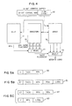
- Figure 4 shows the architecture of the cache as containing, in addition to the DLAT 61, a directory 75 and the cache array 76.
- Each directory entry corresponds to one line in the array.
- the directory entries contain a valid bit, and EX/RO bit and tags which are associated with recognizing a hit, as well as the array set ID.
- the array set ID identifies where in the array 76 the data is stored.
- Each DLAT entry corresponds to one page. In the example of the IBM 3090 series of computers, there are thirty-two lines per page, since one word then contains one bit per line, and a line is 128 bits.
- the virtual address from address buffer 60 addresses each of the DLAT 61, the directory 75 and the cache array 76.
- the array 76 additionally is addressed by the low order offset bits from the address buffer 60.
- the directory 75 provides several RPA cache placement candidates since it is set associative. Four such candidates are illustrated, but the number could vary depending on a specific application.
- the RPA from the DLAT 61 is compared with each of the candidates in the compare circuits 77, and the cache placement output from the compare circuits 77 is used to select the correct output from the array 76.
- Figure 5A illustrates an example of an old DLAT entry 80 as comprising a valid bit (V), tags (a portion of the virtual address), and the real page address (RPA).
- the DLAT entry 81 is modified as shown in Figure 5B to include, in addition to the tags and RPA, status bits (ST), residence bits (RBs), and local change bits (LCBs).
- the DLAT entry 82 includes only the status bits, tags, RPA, and RBs, and a separate, smaller table includes entries 83 containing a valid bit (V), the RPA and LCBs.
- the two approaches illustrated by Figures 5B and 5C are entirely equivalent, the latter being somewhat more complex but with the advantage that the total memory requirements are reduced.
- the operation of the cache is nominal WTWAX with the following exceptions:
- This bit is set to a “1” if the page is held exclusive. Thus, when exclusivity is released, a “1" history bit causes the valid nonresident status to change to exclusive, rather than read only.
Landscapes
- Engineering & Computer Science (AREA)
- Theoretical Computer Science (AREA)
- Physics & Mathematics (AREA)
- General Engineering & Computer Science (AREA)
- General Physics & Mathematics (AREA)
- Memory System Of A Hierarchy Structure (AREA)
Applications Claiming Priority (2)
| Application Number | Priority Date | Filing Date | Title |
|---|---|---|---|
| US07/505,198 US5197139A (en) | 1990-04-05 | 1990-04-05 | Cache management for multi-processor systems utilizing bulk cross-invalidate |
| US505198 | 1990-04-05 |
Publications (2)
| Publication Number | Publication Date |
|---|---|
| EP0450285A2 true EP0450285A2 (de) | 1991-10-09 |
| EP0450285A3 EP0450285A3 (de) | 1992-12-30 |
Family
ID=24009407
Family Applications (1)
| Application Number | Title | Priority Date | Filing Date |
|---|---|---|---|
| EP19910101940 Withdrawn EP0450285A3 (de) | 1990-04-05 | 1991-02-12 | Cache-Speicher |
Country Status (3)
| Country | Link |
|---|---|
| US (1) | US5197139A (de) |
| EP (1) | EP0450285A3 (de) |
| JP (1) | JPH0743670B2 (de) |
Families Citing this family (39)
| Publication number | Priority date | Publication date | Assignee | Title |
|---|---|---|---|---|
| US5361368A (en) * | 1991-09-05 | 1994-11-01 | International Business Machines Corporation | Cross interrogate synchronization mechanism including logic means and delay register |
| US5317738A (en) * | 1992-02-18 | 1994-05-31 | Ncr Corporation | Process affinity scheduling method and apparatus |
| US5493663A (en) * | 1992-04-22 | 1996-02-20 | International Business Machines Corporation | Method and apparatus for predetermining pages for swapping from physical memory in accordance with the number of accesses |
| US5524212A (en) * | 1992-04-27 | 1996-06-04 | University Of Washington | Multiprocessor system with write generate method for updating cache |
| JP2675961B2 (ja) * | 1992-05-20 | 1997-11-12 | インターナショナル・ビジネス・マシーンズ・コーポレイション | 実記憶のページをロックするための方法 |
| US5603008A (en) * | 1992-09-30 | 1997-02-11 | Amdahl Corporation | Computer system having cache memories with independently validated keys in the TLB |
| US5437017A (en) * | 1992-10-09 | 1995-07-25 | International Business Machines Corporation | Method and system for maintaining translation lookaside buffer coherency in a multiprocessor data processing system |
| JP2819982B2 (ja) * | 1993-03-18 | 1998-11-05 | 株式会社日立製作所 | 範囲指定可能なキャッシュ一致保証機能を有するマルチプロセッサシステム |
| US5463750A (en) * | 1993-11-02 | 1995-10-31 | Intergraph Corporation | Method and apparatus for translating virtual addresses in a data processing system having multiple instruction pipelines and separate TLB's |
| US5581704A (en) * | 1993-12-06 | 1996-12-03 | Panasonic Technologies, Inc. | System for maintaining data coherency in cache memory by periodically broadcasting invalidation reports from server to client |
| US5761722A (en) * | 1995-01-30 | 1998-06-02 | Sun Microsystems, Inc. | Method and apparatus for solving the stale data problem occurring in data access performed with data caches |
| US5740400A (en) * | 1995-06-05 | 1998-04-14 | Advanced Micro Devices Inc. | Reducing cache snooping overhead in a multilevel cache system with multiple bus masters and a shared level two cache by using an inclusion field |
| US5924125A (en) * | 1995-08-01 | 1999-07-13 | Arya; Siamak | Method and apparatus for parallel access to consecutive TLB entries |
| US6098128A (en) | 1995-09-18 | 2000-08-01 | Cyberstorage Systems Corporation | Universal storage management system |
| US5778437A (en) * | 1995-09-25 | 1998-07-07 | International Business Machines Corporation | Invalidation bus optimization for multiprocessors using directory-based cache coherence protocols in which an address of a line to be modified is placed on the invalidation bus simultaneously with sending a modify request to the directory |
| US5787486A (en) * | 1995-12-15 | 1998-07-28 | International Business Machines Corporation | Bus protocol for locked cycle cache hit |
| US5680571A (en) * | 1995-12-28 | 1997-10-21 | Unisys Corporation | Multi-processor data processing system with multiple, separate instruction and operand second level caches |
| US6070233A (en) * | 1996-01-26 | 2000-05-30 | Unisys Corporation | Processor bus traffic optimization system for multi-level cache utilizing reflection status bit to indicate data inclusion in higher level cache |
| US5790774A (en) * | 1996-05-21 | 1998-08-04 | Storage Computer Corporation | Data storage system with dedicated allocation of parity storage and parity reads and writes only on operations requiring parity information |
| US5787477A (en) * | 1996-06-18 | 1998-07-28 | International Business Machines Corporation | Multi-processor cache coherency protocol allowing asynchronous modification of cache data |
| US5900015A (en) * | 1996-08-09 | 1999-05-04 | International Business Machines Corporation | System and method for maintaining cache coherency using path directories |
| US5897655A (en) * | 1996-12-10 | 1999-04-27 | International Business Machines Corporation | System and method for cache replacement within a cache set based on valid, modified or least recently used status in order of preference |
| US5960455A (en) * | 1996-12-30 | 1999-09-28 | Unisys Corporation | Scalable cross bar type storage controller |
| US5875201A (en) * | 1996-12-30 | 1999-02-23 | Unisys Corporation | Second level cache having instruction cache parity error control |
| US6122711A (en) | 1997-01-07 | 2000-09-19 | Unisys Corporation | Method of and apparatus for store-in second level cache flush |
| US5860093A (en) * | 1997-01-21 | 1999-01-12 | Unisys Corporation | Reduced instruction processor/storage controller interface |
| US6000015A (en) * | 1997-09-16 | 1999-12-07 | Unisys Corporation | Processor bus traffic optimization system for multi-level cache utilizing reflection status bit to indicate data inclusion in a higher level cache |
| US6725334B2 (en) * | 2000-06-09 | 2004-04-20 | Hewlett-Packard Development Company, L.P. | Method and system for exclusive two-level caching in a chip-multiprocessor |
| US20070180193A1 (en) * | 2006-01-30 | 2007-08-02 | International Business Machines Corporation | History based line install |
| US20070260754A1 (en) * | 2006-04-13 | 2007-11-08 | Irish John D | Hardware Assisted Exception for Software Miss Handling of an I/O Address Translation Cache Miss |
| US7877537B2 (en) * | 2006-12-15 | 2011-01-25 | Microchip Technology Incorporated | Configurable cache for a microprocessor |
| US9208095B2 (en) | 2006-12-15 | 2015-12-08 | Microchip Technology Incorporated | Configurable cache for a microprocessor |
| US7966457B2 (en) | 2006-12-15 | 2011-06-21 | Microchip Technology Incorporated | Configurable cache for a microprocessor |
| US8285969B2 (en) * | 2009-09-02 | 2012-10-09 | International Business Machines Corporation | Reducing broadcasts in multiprocessors |
| US9384133B2 (en) | 2014-05-30 | 2016-07-05 | International Business Machines Corporation | Synchronizing updates of page table status indicators and performing bulk operations |
| US9785554B2 (en) * | 2014-05-30 | 2017-10-10 | International Business Machines Corporation | Synchronizing updates of page table status indicators in a multiprocessing environment |
| EP3249539B1 (de) * | 2015-02-16 | 2021-08-18 | Huawei Technologies Co., Ltd. | Verfahren und vorrichtung zum zugreifen auf ein datenbesucherverzeichnis in einem mehrkernsystem |
| US10733171B2 (en) | 2018-04-03 | 2020-08-04 | Sap Se | Database lock management with cache-optimized hash table |
| US10761856B2 (en) | 2018-07-19 | 2020-09-01 | International Business Machines Corporation | Instruction completion table containing entries that share instruction tags |
Family Cites Families (31)
| Publication number | Priority date | Publication date | Assignee | Title |
|---|---|---|---|---|
| US3735360A (en) * | 1971-08-25 | 1973-05-22 | Ibm | High speed buffer operation in a multi-processing system |
| US4142234A (en) * | 1977-11-28 | 1979-02-27 | International Business Machines Corporation | Bias filter memory for filtering out unnecessary interrogations of cache directories in a multiprocessor system |
| JPS5733471A (en) * | 1980-07-31 | 1982-02-23 | Fujitsu Ltd | Memory access control system for multiprocessor |
| US4399506A (en) * | 1980-10-06 | 1983-08-16 | International Business Machines Corporation | Store-in-cache processor means for clearing main storage |
| US4400770A (en) * | 1980-11-10 | 1983-08-23 | International Business Machines Corporation | Cache synonym detection and handling means |
| US4394731A (en) * | 1980-11-10 | 1983-07-19 | International Business Machines Corporation | Cache storage line shareability control for a multiprocessor system |
| US4513367A (en) * | 1981-03-23 | 1985-04-23 | International Business Machines Corporation | Cache locking controls in a multiprocessor |
| US4445174A (en) * | 1981-03-31 | 1984-04-24 | International Business Machines Corporation | Multiprocessing system including a shared cache |
| US4464712A (en) * | 1981-07-06 | 1984-08-07 | International Business Machines Corporation | Second level cache replacement method and apparatus |
| US4484267A (en) * | 1981-12-30 | 1984-11-20 | International Business Machines Corporation | Cache sharing control in a multiprocessor |
| US4463420A (en) * | 1982-02-23 | 1984-07-31 | International Business Machines Corporation | Multiprocessor cache replacement under task control |
| US4503497A (en) * | 1982-05-27 | 1985-03-05 | International Business Machines Corporation | System for independent cache-to-cache transfer |
| JPS5994289A (ja) * | 1982-11-22 | 1984-05-30 | Hitachi Ltd | 記憶制御方式 |
| US4622631B1 (en) * | 1983-12-30 | 1996-04-09 | Recognition Int Inc | Data processing system having a data coherence solution |
| US4654778A (en) * | 1984-06-27 | 1987-03-31 | International Business Machines Corporation | Direct parallel path for storage accesses unloading common system path |
| DE3686291T2 (de) * | 1985-05-29 | 1993-03-11 | Toshiba Computer Eng | Cache-anordnung mit einem lru-verfahren und magnetscheibensteuereinrichtung mit einer solchen anordnung. |
| US4755930A (en) * | 1985-06-27 | 1988-07-05 | Encore Computer Corporation | Hierarchical cache memory system and method |
| US4775955A (en) * | 1985-10-30 | 1988-10-04 | International Business Machines Corporation | Cache coherence mechanism based on locking |
| US4797814A (en) * | 1986-05-01 | 1989-01-10 | International Business Machines Corporation | Variable address mode cache |
| JPS63231650A (ja) * | 1987-03-20 | 1988-09-27 | Fujitsu Ltd | キヤツシユメモリ制御方式 |
| US4991090A (en) * | 1987-05-18 | 1991-02-05 | International Business Machines Corporation | Posting out-of-sequence fetches |
| JPS6412348A (en) * | 1987-07-06 | 1989-01-17 | Hitachi Ltd | Buffer control system |
| US5025366A (en) * | 1988-01-20 | 1991-06-18 | Advanced Micro Devices, Inc. | Organization of an integrated cache unit for flexible usage in cache system design |
| US5023776A (en) * | 1988-02-22 | 1991-06-11 | International Business Machines Corp. | Store queue for a tightly coupled multiple processor configuration with two-level cache buffer storage |
| US4977498A (en) * | 1988-04-01 | 1990-12-11 | Digital Equipment Corporation | Data processing system having a data memory interlock coherency scheme |
| US5032985A (en) * | 1988-07-21 | 1991-07-16 | International Business Machines Corporation | Multiprocessor system with memory fetch buffer invoked during cross-interrogation |
| JP2961663B2 (ja) * | 1988-08-01 | 1999-10-12 | 日本電信電話株式会社 | キャッシュメモリ制御方法 |
| US4928225A (en) * | 1988-08-25 | 1990-05-22 | Edgcore Technology, Inc. | Coherent cache structures and methods |
| US5029070A (en) * | 1988-08-25 | 1991-07-02 | Edge Computer Corporation | Coherent cache structures and methods |
| JPH0290259A (ja) * | 1988-09-27 | 1990-03-29 | Hitachi Ltd | マルチプロセッサシステム |
| US5016168A (en) * | 1988-12-23 | 1991-05-14 | International Business Machines Corporation | Method for storing into non-exclusive cache lines in multiprocessor systems |
-
1990
- 1990-04-05 US US07/505,198 patent/US5197139A/en not_active Expired - Fee Related
-
1991
- 1991-02-12 EP EP19910101940 patent/EP0450285A3/de not_active Withdrawn
- 1991-03-25 JP JP3082991A patent/JPH0743670B2/ja not_active Expired - Lifetime
Also Published As
| Publication number | Publication date |
|---|---|
| US5197139A (en) | 1993-03-23 |
| EP0450285A3 (de) | 1992-12-30 |
| JPH0743670B2 (ja) | 1995-05-15 |
| JPH04227552A (ja) | 1992-08-17 |
Similar Documents
| Publication | Publication Date | Title |
|---|---|---|
| US5197139A (en) | Cache management for multi-processor systems utilizing bulk cross-invalidate | |
| US5230070A (en) | Access authorization table for multi-processor caches | |
| EP0062165B1 (de) | Mehrprozessoren mit privaten und gemeinsam benutzten Pufferspeichern | |
| US5317716A (en) | Multiple caches using state information indicating if cache line was previously modified and type of access rights granted to assign access rights to cache line | |
| US6370622B1 (en) | Method and apparatus for curious and column caching | |
| US4394731A (en) | Cache storage line shareability control for a multiprocessor system | |
| US4400770A (en) | Cache synonym detection and handling means | |
| US5155824A (en) | System for transferring selected data words between main memory and cache with multiple data words and multiple dirty bits for each address | |
| US6625698B2 (en) | Method and apparatus for controlling memory storage locks based on cache line ownership | |
| CA1238984A (en) | Cooperative memory hierarchy | |
| US6868485B1 (en) | Computer system with integrated directory and processor cache | |
| US5450563A (en) | Storage protection keys in two level cache system | |
| US5148533A (en) | Apparatus and method for data group coherency in a tightly coupled data processing system with plural execution and data cache units | |
| US5119485A (en) | Method for data bus snooping in a data processing system by selective concurrent read and invalidate cache operation | |
| US7814285B2 (en) | Method and apparatus for filtering memory write snoop activity in a distributed shared memory computer | |
| US6587931B1 (en) | Directory-based cache coherency system supporting multiple instruction processor and input/output caches | |
| US5210848A (en) | Multi-processor caches with large granularity exclusivity locking | |
| EP0325419A2 (de) | Verfahren und Vorrichtung zum Schreiben gegenseitiger verriegelter Variablen in einen integrierten Cachespeicher | |
| EP0372201B1 (de) | Verfahren zum Abrufen von potentiell ungültigen Daten in einem Mehrrechnersystem | |
| US6351795B1 (en) | Selective address translation in coherent memory replication | |
| US5214766A (en) | Data prefetching based on store information in multi-processor caches | |
| US5909697A (en) | Reducing cache misses by snarfing writebacks in non-inclusive memory systems | |
| US5835714A (en) | Method and apparatus for reservation of data buses between multiple storage control elements | |
| US5987544A (en) | System interface protocol with optional module cache | |
| US5737575A (en) | Interleaved key memory with multi-page key cache |
Legal Events
| Date | Code | Title | Description |
|---|---|---|---|
| PUAI | Public reference made under article 153(3) epc to a published international application that has entered the european phase |
Free format text: ORIGINAL CODE: 0009012 |
|
| AK | Designated contracting states |
Kind code of ref document: A2 Designated state(s): DE FR GB |
|
| 17P | Request for examination filed |
Effective date: 19911219 |
|
| PUAL | Search report despatched |
Free format text: ORIGINAL CODE: 0009013 |
|
| AK | Designated contracting states |
Kind code of ref document: A3 Designated state(s): DE FR GB |
|
| STAA | Information on the status of an ep patent application or granted ep patent |
Free format text: STATUS: THE APPLICATION HAS BEEN WITHDRAWN |
|
| 18W | Application withdrawn |
Withdrawal date: 19970410 |