EP0450571A2 - Détecteur ultra-rapide pour imagerie en rayons X - Google Patents
Détecteur ultra-rapide pour imagerie en rayons X Download PDFInfo
- Publication number
- EP0450571A2 EP0450571A2 EP91105189A EP91105189A EP0450571A2 EP 0450571 A2 EP0450571 A2 EP 0450571A2 EP 91105189 A EP91105189 A EP 91105189A EP 91105189 A EP91105189 A EP 91105189A EP 0450571 A2 EP0450571 A2 EP 0450571A2
- Authority
- EP
- European Patent Office
- Prior art keywords
- photocathode
- ray
- electron
- electrons
- avalanche
- Prior art date
- Legal status (The legal status is an assumption and is not a legal conclusion. Google has not performed a legal analysis and makes no representation as to the accuracy of the status listed.)
- Ceased
Links
- 238000003384 imaging method Methods 0.000 title description 26
- 230000005855 radiation Effects 0.000 claims abstract description 25
- 230000004044 response Effects 0.000 claims abstract description 20
- 238000000034 method Methods 0.000 claims description 73
- 238000001514 detection method Methods 0.000 claims description 31
- 238000000429 assembly Methods 0.000 claims description 27
- 230000000712 assembly Effects 0.000 claims description 27
- 238000002601 radiography Methods 0.000 claims description 7
- 238000002405 diagnostic procedure Methods 0.000 claims description 2
- 239000007789 gas Substances 0.000 description 77
- 230000003321 amplification Effects 0.000 description 63
- 238000003199 nucleic acid amplification method Methods 0.000 description 63
- 238000012546 transfer Methods 0.000 description 31
- 230000003287 optical effect Effects 0.000 description 21
- LCGLNKUTAGEVQW-UHFFFAOYSA-N Dimethyl ether Chemical compound COC LCGLNKUTAGEVQW-UHFFFAOYSA-N 0.000 description 18
- 239000000203 mixture Substances 0.000 description 18
- 230000004907 flux Effects 0.000 description 17
- 238000000926 separation method Methods 0.000 description 17
- 238000006243 chemical reaction Methods 0.000 description 15
- 238000009826 distribution Methods 0.000 description 15
- 239000000463 material Substances 0.000 description 15
- 230000008569 process Effects 0.000 description 15
- 230000004807 localization Effects 0.000 description 14
- 239000011888 foil Substances 0.000 description 12
- 150000002500 ions Chemical class 0.000 description 12
- 229910052751 metal Inorganic materials 0.000 description 10
- 239000002184 metal Substances 0.000 description 10
- 230000032683 aging Effects 0.000 description 9
- 239000007787 solid Substances 0.000 description 9
- 238000002474 experimental method Methods 0.000 description 8
- PCHJSUWPFVWCPO-UHFFFAOYSA-N gold Chemical compound [Au] PCHJSUWPFVWCPO-UHFFFAOYSA-N 0.000 description 8
- 229910052737 gold Inorganic materials 0.000 description 8
- 239000010931 gold Substances 0.000 description 8
- 238000011160 research Methods 0.000 description 8
- OTMSDBZUPAUEDD-UHFFFAOYSA-N Ethane Chemical compound CC OTMSDBZUPAUEDD-UHFFFAOYSA-N 0.000 description 7
- 230000000875 corresponding effect Effects 0.000 description 7
- 238000009792 diffusion process Methods 0.000 description 7
- RYGMFSIKBFXOCR-UHFFFAOYSA-N Copper Chemical compound [Cu] RYGMFSIKBFXOCR-UHFFFAOYSA-N 0.000 description 6
- 239000004020 conductor Substances 0.000 description 6
- 229910052802 copper Inorganic materials 0.000 description 6
- 239000010949 copper Substances 0.000 description 6
- 229910052782 aluminium Inorganic materials 0.000 description 5
- XAGFODPZIPBFFR-UHFFFAOYSA-N aluminium Chemical compound [Al] XAGFODPZIPBFFR-UHFFFAOYSA-N 0.000 description 5
- 238000003491 array Methods 0.000 description 5
- 230000000694 effects Effects 0.000 description 5
- 238000004611 spectroscopical analysis Methods 0.000 description 5
- 239000004593 Epoxy Substances 0.000 description 4
- 238000000342 Monte Carlo simulation Methods 0.000 description 4
- 239000004743 Polypropylene Substances 0.000 description 4
- 238000000441 X-ray spectroscopy Methods 0.000 description 4
- 238000010521 absorption reaction Methods 0.000 description 4
- 238000004458 analytical method Methods 0.000 description 4
- 229910001632 barium fluoride Inorganic materials 0.000 description 4
- 230000008901 benefit Effects 0.000 description 4
- 229920003223 poly(pyromellitimide-1,4-diphenyl ether) Polymers 0.000 description 4
- -1 polypropylene Polymers 0.000 description 4
- 229920001155 polypropylene Polymers 0.000 description 4
- 230000035945 sensitivity Effects 0.000 description 4
- 238000001228 spectrum Methods 0.000 description 4
- 229910001220 stainless steel Inorganic materials 0.000 description 4
- 239000010935 stainless steel Substances 0.000 description 4
- 239000000126 substance Substances 0.000 description 4
- 229920002799 BoPET Polymers 0.000 description 3
- 239000005041 Mylar™ Substances 0.000 description 3
- 238000002441 X-ray diffraction Methods 0.000 description 3
- 230000008878 coupling Effects 0.000 description 3
- 238000010168 coupling process Methods 0.000 description 3
- 238000005859 coupling reaction Methods 0.000 description 3
- 238000004519 manufacturing process Methods 0.000 description 3
- 238000005259 measurement Methods 0.000 description 3
- 239000002245 particle Substances 0.000 description 3
- 239000000758 substrate Substances 0.000 description 3
- 230000005469 synchrotron radiation Effects 0.000 description 3
- LFQSCWFLJHTTHZ-UHFFFAOYSA-N Ethanol Chemical compound CCO LFQSCWFLJHTTHZ-UHFFFAOYSA-N 0.000 description 2
- KFZMGEQAYNKOFK-UHFFFAOYSA-N Isopropanol Chemical compound CC(C)O KFZMGEQAYNKOFK-UHFFFAOYSA-N 0.000 description 2
- 229920000134 Metallised film Polymers 0.000 description 2
- 230000005540 biological transmission Effects 0.000 description 2
- WUKWITHWXAAZEY-UHFFFAOYSA-L calcium difluoride Chemical compound [F-].[F-].[Ca+2] WUKWITHWXAAZEY-UHFFFAOYSA-L 0.000 description 2
- 229910001634 calcium fluoride Inorganic materials 0.000 description 2
- JJWKPURADFRFRB-UHFFFAOYSA-N carbonyl sulfide Chemical compound O=C=S JJWKPURADFRFRB-UHFFFAOYSA-N 0.000 description 2
- 230000008859 change Effects 0.000 description 2
- 239000013078 crystal Substances 0.000 description 2
- 238000011161 development Methods 0.000 description 2
- 230000018109 developmental process Effects 0.000 description 2
- 230000005684 electric field Effects 0.000 description 2
- 239000003822 epoxy resin Substances 0.000 description 2
- 235000019441 ethanol Nutrition 0.000 description 2
- 238000001704 evaporation Methods 0.000 description 2
- 230000008020 evaporation Effects 0.000 description 2
- 230000003993 interaction Effects 0.000 description 2
- NNPPMTNAJDCUHE-UHFFFAOYSA-N isobutane Chemical compound CC(C)C NNPPMTNAJDCUHE-UHFFFAOYSA-N 0.000 description 2
- 229910001120 nichrome Inorganic materials 0.000 description 2
- 238000012634 optical imaging Methods 0.000 description 2
- BASFCYQUMIYNBI-UHFFFAOYSA-N platinum Chemical compound [Pt] BASFCYQUMIYNBI-UHFFFAOYSA-N 0.000 description 2
- 229920000647 polyepoxide Polymers 0.000 description 2
- 102000004169 proteins and genes Human genes 0.000 description 2
- 108090000623 proteins and genes Proteins 0.000 description 2
- 238000011002 quantification Methods 0.000 description 2
- 238000012216 screening Methods 0.000 description 2
- 238000005211 surface analysis Methods 0.000 description 2
- 230000009897 systematic effect Effects 0.000 description 2
- 238000013519 translation Methods 0.000 description 2
- WFKWXMTUELFFGS-UHFFFAOYSA-N tungsten Chemical compound [W] WFKWXMTUELFFGS-UHFFFAOYSA-N 0.000 description 2
- 229910052721 tungsten Inorganic materials 0.000 description 2
- 239000010937 tungsten Substances 0.000 description 2
- 238000011144 upstream manufacturing Methods 0.000 description 2
- XJKSTNDFUHDPQJ-UHFFFAOYSA-N 1,4-diphenylbenzene Chemical group C1=CC=CC=C1C1=CC=C(C=2C=CC=CC=2)C=C1 XJKSTNDFUHDPQJ-UHFFFAOYSA-N 0.000 description 1
- 229920004439 Aclar® Polymers 0.000 description 1
- OKTJSMMVPCPJKN-UHFFFAOYSA-N Carbon Chemical compound [C] OKTJSMMVPCPJKN-UHFFFAOYSA-N 0.000 description 1
- 239000004215 Carbon black (E152) Substances 0.000 description 1
- 241000252095 Congridae Species 0.000 description 1
- 229920004943 Delrin® Polymers 0.000 description 1
- 206010065042 Immune reconstitution inflammatory syndrome Diseases 0.000 description 1
- 241000551546 Minerva Species 0.000 description 1
- 239000004677 Nylon Substances 0.000 description 1
- 229910004489 SiLi Inorganic materials 0.000 description 1
- 239000011358 absorbing material Substances 0.000 description 1
- 150000001298 alcohols Chemical class 0.000 description 1
- 238000013459 approach Methods 0.000 description 1
- XQPRBTXUXXVTKB-UHFFFAOYSA-M caesium iodide Chemical compound [I-].[Cs+] XQPRBTXUXXVTKB-UHFFFAOYSA-M 0.000 description 1
- 238000004364 calculation method Methods 0.000 description 1
- 229910052799 carbon Inorganic materials 0.000 description 1
- 238000005094 computer simulation Methods 0.000 description 1
- 230000005493 condensed matter Effects 0.000 description 1
- 230000001276 controlling effect Effects 0.000 description 1
- 238000012937 correction Methods 0.000 description 1
- 230000002596 correlated effect Effects 0.000 description 1
- 238000010219 correlation analysis Methods 0.000 description 1
- 238000005314 correlation function Methods 0.000 description 1
- 238000002425 crystallisation Methods 0.000 description 1
- 230000008025 crystallization Effects 0.000 description 1
- 238000007405 data analysis Methods 0.000 description 1
- 230000007423 decrease Effects 0.000 description 1
- 230000007547 defect Effects 0.000 description 1
- 230000001419 dependent effect Effects 0.000 description 1
- 238000000151 deposition Methods 0.000 description 1
- 230000006866 deterioration Effects 0.000 description 1
- 238000002050 diffraction method Methods 0.000 description 1
- NKDDWNXOKDWJAK-UHFFFAOYSA-N dimethoxymethane Chemical compound COCOC NKDDWNXOKDWJAK-UHFFFAOYSA-N 0.000 description 1
- 239000003814 drug Substances 0.000 description 1
- 238000010894 electron beam technology Methods 0.000 description 1
- 230000005284 excitation Effects 0.000 description 1
- 238000000605 extraction Methods 0.000 description 1
- 239000000835 fiber Substances 0.000 description 1
- 239000012530 fluid Substances 0.000 description 1
- 238000011010 flushing procedure Methods 0.000 description 1
- 230000004927 fusion Effects 0.000 description 1
- 238000000574 gas--solid chromatography Methods 0.000 description 1
- 229910002804 graphite Inorganic materials 0.000 description 1
- 239000010439 graphite Substances 0.000 description 1
- 230000005484 gravity Effects 0.000 description 1
- 229930195733 hydrocarbon Natural products 0.000 description 1
- 238000005286 illumination Methods 0.000 description 1
- 238000009434 installation Methods 0.000 description 1
- 239000012212 insulator Substances 0.000 description 1
- 238000000752 ionisation method Methods 0.000 description 1
- 230000001678 irradiating effect Effects 0.000 description 1
- 239000001282 iso-butane Substances 0.000 description 1
- 230000033001 locomotion Effects 0.000 description 1
- 238000005461 lubrication Methods 0.000 description 1
- VNWKTOKETHGBQD-UHFFFAOYSA-N methane Chemical compound C VNWKTOKETHGBQD-UHFFFAOYSA-N 0.000 description 1
- 238000012544 monitoring process Methods 0.000 description 1
- 210000003205 muscle Anatomy 0.000 description 1
- 239000004081 narcotic agent Substances 0.000 description 1
- 229910052756 noble gas Inorganic materials 0.000 description 1
- 150000002835 noble gases Chemical class 0.000 description 1
- 239000012811 non-conductive material Substances 0.000 description 1
- 238000009206 nuclear medicine Methods 0.000 description 1
- 229920001778 nylon Polymers 0.000 description 1
- 239000013307 optical fiber Substances 0.000 description 1
- 229930184652 p-Terphenyl Natural products 0.000 description 1
- 239000003973 paint Substances 0.000 description 1
- 230000005433 particle physics related processes and functions Effects 0.000 description 1
- 238000009304 pastoral farming Methods 0.000 description 1
- 229910052697 platinum Inorganic materials 0.000 description 1
- 229920000052 poly(p-xylylene) Polymers 0.000 description 1
- 239000005023 polychlorotrifluoroethylene (PCTFE) polymer Substances 0.000 description 1
- 229920000642 polymer Polymers 0.000 description 1
- 239000011148 porous material Substances 0.000 description 1
- 238000005086 pumping Methods 0.000 description 1
- 238000000746 purification Methods 0.000 description 1
- 238000003908 quality control method Methods 0.000 description 1
- 239000010453 quartz Substances 0.000 description 1
- 230000006798 recombination Effects 0.000 description 1
- 238000005215 recombination Methods 0.000 description 1
- 230000009467 reduction Effects 0.000 description 1
- 238000012552 review Methods 0.000 description 1
- 229910052594 sapphire Inorganic materials 0.000 description 1
- 239000010980 sapphire Substances 0.000 description 1
- 239000004065 semiconductor Substances 0.000 description 1
- VYPSYNLAJGMNEJ-UHFFFAOYSA-N silicon dioxide Inorganic materials O=[Si]=O VYPSYNLAJGMNEJ-UHFFFAOYSA-N 0.000 description 1
- 238000005476 soldering Methods 0.000 description 1
- 125000006850 spacer group Chemical group 0.000 description 1
- 238000010561 standard procedure Methods 0.000 description 1
- 230000003068 static effect Effects 0.000 description 1
- 230000001629 suppression Effects 0.000 description 1
- 230000004083 survival effect Effects 0.000 description 1
- 229910052715 tantalum Inorganic materials 0.000 description 1
- GUVRBAGPIYLISA-UHFFFAOYSA-N tantalum atom Chemical compound [Ta] GUVRBAGPIYLISA-UHFFFAOYSA-N 0.000 description 1
- TXEYQDLBPFQVAA-UHFFFAOYSA-N tetrafluoromethane Chemical compound FC(F)(F)F TXEYQDLBPFQVAA-UHFFFAOYSA-N 0.000 description 1
- 230000001225 therapeutic effect Effects 0.000 description 1
- 238000003325 tomography Methods 0.000 description 1
- 238000012876 topography Methods 0.000 description 1
- 230000005472 transition radiation Effects 0.000 description 1
- 238000007738 vacuum evaporation Methods 0.000 description 1
- 238000001429 visible spectrum Methods 0.000 description 1
- 238000004846 x-ray emission Methods 0.000 description 1
- 238000003963 x-ray microscopy Methods 0.000 description 1
- 229910052724 xenon Inorganic materials 0.000 description 1
- FHNFHKCVQCLJFQ-UHFFFAOYSA-N xenon atom Chemical compound [Xe] FHNFHKCVQCLJFQ-UHFFFAOYSA-N 0.000 description 1
Images







Classifications
-
- H—ELECTRICITY
- H01—ELECTRIC ELEMENTS
- H01J—ELECTRIC DISCHARGE TUBES OR DISCHARGE LAMPS
- H01J47/00—Tubes for determining the presence, intensity, density or energy of radiation or particles
- H01J47/02—Ionisation chambers
Definitions
- the present invention relates to detectors generally and more particularly to X-ray detectors.
- X-ray detectors include varieties of gas-filled imaging detectors which are based on the conversion of X-ray photons in the gas volume to electrons and on the proportional amplification of the released photoelectrons in various wire electrode assemblies. Such detectors are described by J.E. Bateman in "Detectors for Condensed Matter Studies", Nuclear Instruments and Methods, A273 (1988) 721-730. Bateman also describes other X-ray photon detectors such as various solid scintillators and semiconductor devices.
- Gas-filled detectors are by far the most efficient and flexible X-ray detectors. They offer high localization resolution and good linearity, moderate-to-high counting rate capability, and a large variety of geometries over large active areas.
- gaseous (gas filled) detectors have the following disadvantages:
- Detectors having a relatively rapid response capable of operating at high X-ray flux are important in applications such as X-ray diffraction analysis in synchrotron radiation accelerators and X-ray radiography with intense X-ray generators.
- Fast detectors are also important when time correlated information is needed, as in the study of dynamic processes, as described in A.R. Faruqi, Nuclear Instruments and Methods, A273 (1988) 754.
- Efficiency of X-ray detectors is exceedingly important, since any increase in efficiency enables X-ray dosages applied to subjects in therapeutic and diagnostic applications to be correspondingly reduced.
- the present invention seeks to provide an improved X-ray detector, which is characterized by high detection efficiency and speed, the capability to operate at high X-ray fluxes and to provide high two dimensional imaging accuracy.
- an X-ray detector including a photocathode arranged to receive X-ray radiation and being operative to provide in response thereto an output of electrons, and at least one electron multiplier operative at subatmospheric pressure and in response to the output of electrons from the photocathode to provide an avalanche including an increased number of electrons.
- the electron multiplier is operative at any suitable (not necessarily subatmospheric) pressure and the electron multiplier may be a multistage electron multiplier.
- an electrode and a readout system for detecting the electrons produced by the electron multiplier or alternatively, an optical recording system which records photons produced during the electron multiplication process.
- the photodetector includes one or more photocathode foils, which may be formed of Csl, Cul, Au, Ta etc.
- the photodetector may include a porous or amorphous material such as Csl having typically 1 % - 3% of the bulk density.
- the electron multiplier includes a large area, preferably relatively low-pressure multistage chamber, with various electrode geometries and readout methods.
- the chamber may be at any suitable pressure.
- the X-ray detector includes at least one detecting means for detecting an indication of at least one characteristic of the electron avalanche produced by the electron multiplier.
- the at least one electron multiplier includes at least one detecting means for detecting an indication of at least one characteristic of the electron avalanche produced by the electron multiplier.
- the X-ray detector also includes a large area chamber and at least the photocathode and the at least one electron multiplier are located interiorly of the chamber. Still further in accordance with a preferred embodiment of the present invention, a non-aging high gain-providing gas is provided interiorly of the chamber.
- the electron multiplier defines at least one amplification stage and at least one transfer stage.
- the at least one amplification stage includes at least two amplification stages.
- At least one of the at least one transfer stages is defined before the at least one amplification stage.
- the at least one transfer stage includes a plurality of transfer stages.
- the plurality of transfer stages includes at least three transfer stages.
- At least one of the at least one transfer stages is defined after the amplification stage.
- the electron multiplier includes at least one gate electrode before at least one of the least one amplification stages for receiving a selected one of at least two selectable voltage levels.
- the at least one gate electrode includes at least two gate electrodes.
- the electron multiplier also defines a pre-amplification stage before the amplification stage.
- At least one of the at least one transfer stages is defined before the preamplification stage and the at least one amplification stage.
- the detecting means includes electron detection means for detecting the electrons produced by the electron avalanche.
- the electron detection means includes a plurality of pad electrode assemblies for collecting the electrons produced by the electron multiplier.
- each of the pad electrode assemblies includes a pad electrode, an insulative layer and a resistive layer.
- the electron detection means includes at least one strip electrode array, the strip electrode array including a first plurality of mutually parallel strip electrodes, generally planar insulating means, defining a plane generally parallel to the first plurality of mutually parallel strip electrodes and a second plurality of mutually parallel strip electrodes, arranged generally parallel to the plane and generally perpendicular to the first plurality of strip electrodes.
- the detecting means includes photon detection means for detecting photons emitted during the electron avalanche.
- the photocathode is generally planar and is configured and arranged to receive X-ray radiation impinging on both sides thereof.
- the at least one electron multiplier includes two electron multipliers.
- the at least one detecting means includes two detecting means.
- the at least one electron multiplier includes two electron multipliers disposed respectively on the two sides of the planar photocathode.
- the at least one detecting means includes two detection means disposed respectively on the two sides of the planar photocathode.
- the photocathode includes a metal foil.
- the photocathode includes an insulative support layer and at least one semiconductive layers disposed on respective at least one sides of the support layer.
- the photocathode includes an insulative support layer and at least one conductive layers disposed on respective at least one sides of the support layer.
- the photocathode includes a conductive support layer and at least one insulative layer disposed on respective at least one sides of the support layer.
- the photocathode includes a conductive support layer and at least one semiconductive layer disposed on respective at least one sides of the support layer.
- the photocathode includes an insulative support layer and at least one noninsulative element disposed on respective at least one sides of the support layer, each noninsulative element including a semiconductive layer and a conductive layer.
- the photocathode includes an insulative support layer and at least one photocathode element disposed on respective at least one sides of the support layer, each photocathode element including an insulative layer and a conductive layer.
- the photocathode includes a conductive support layer and at least one low-density non-conductive layers disposed on respective at least one sides of the support layer.
- the photocathode includes a support layer and at least one photocathode element disposed on respective at least one sides of the support layer, each photocathode element including a metal layer and a nonconductive layer.
- the photocathode includes a porous material.
- the at least one characteristic includes at least one of the following characteristics: the number of electrons in the avalanche, the location of the avalanche, and the time of occurrence of the avalanche.
- the gas is generally light-emitting.
- the at least one detecting means includes at least one electrode for providing the avalanche and for providing the indication of the at least one characteristic of the electron avalanche.
- the at least one electrode includes a plurality of conductive elements.
- the plurality of conductive elements includes a plurality of wires.
- an X-ray detector assembly including a gas filled enclosure and a plurality of X-ray detectors located interiorly of the gas filled enclosure, each individual one of the plurality of X-ray detectors preferably being constructed and operative as above.
- an X-ray detecting method including the steps of providing a photocathode arranged to receive X-ray radiation and being operative to provide in response thereto an output of electrons, and, in response to the output of electrons from the photocathode, providing at sub-atmospheric pressure an avalanche including an increased number of electrons.
- the method also includes the step of detecting an indication of at least one characteristic of the electron avalanche.
- Fig. 1A illustrates an X-ray detector constructed and operative in accordance with a preferred embodiment of the present invention.
- the X-ray detector indicated generally by reference numeral 10 comprises a preferably low-pressure gas filled enclosure 12 including a gas entry conduit 13, an X-ray photon entrance window 14, and a gas exit conduit 15.
- the circulated gas is typically at approximately 20 Torr pressure and at stabilized room temperature. Alternatively, the apparatus can operate at any other suitable pressure.
- the examples set forth hereinbelow are directed to subatmospheric pressure applications.
- Entrance window 14 is typically formed of polypropylene or of Mylar or Kapton foil and is supported on a frame 16.
- the thickness of the foil may vary as a function of the energy of the impinging X-ray photons. For example, for photons of energy 10 KeV, a preferred thickness would be 5-10 microns.
- the impingement of the X-ray photons on the photocathode 20 causes the release of electrons from the photocathode at the location of the impingement.
- the released electrons are amplified in a pre-amplification stage 22 to produce an initial avalanche, as illustrated by reference numeral 24.
- the electron avalanche is transferred via a transfer gap 26 to an amplification stage 28, which produces a second avalanche 30.
- the electrons in second avalanche 30 are transferred through a second transfer stage 32 and are collected by an array 34 of pad electrodes 36.
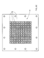
- a typical configuration of array 34 of pad electrodes 36 is shown in Fig. 3C.
- the pad electrodes are typically of square configuration and of side length 2 - 10 mm.
- Preferably the pad electrodes 36 are separated from adjacent pad electrodes by 0.1 - 0.3 mm.
- the pad electrodes are preferably formed of copper formed over an epoxy laminated printed circuit board.
- the output signals of electrodes 36 are transmitted via conductors 38 to readout electronics 40, as described in P. Fischer et al., IEEE Trans. Nucl. Sci. NS-35 (1988), p. 432 onward, the disclosure of which is incorporated herein by reference.
- the electronic information from detector 10 is preferably computer processed to obtain values for integral charge and for center of gravity, using known methods and a suitable computer such as a Microvax II, commercially available from Digital Equipment Corporation, where it is stored and processed for data analysis
- the structure downstream of the photocathode 20 is an electron multiplier.
- the photocathode 20 receives a negative voltage via a conductor 42, which is coupled to a voltage source (not shown) via an insulative connector 44.
- the pre-amplification stage 22 is also defined by a mesh electrode 46, which typically is maintained at a desired voltage by means of a conductor 48 coupled to a voltage source (not shown) via an insulative connector 50.
- Typical voltages and gap separations at these stages for a typical gas pressure of 20 Torr are as follows:
- a preferred level of potential for the readout electrodes 36 is 0 volts.
- the preferred levels of potential for the photocathode 20 and for the respective electrodes 46, 52, 54, and 36 of each stage are:
- the gas here and in the embodiments of the present invention shown in Figs. 1 B - 11 may comprise any suitable gas which, at relatively low pressure, is non-aging and provides high gain (i.e. high amplification).
- Typical gases having these characteristics are: dimethylether, isobutane, CF 4 , CH 4 , C 2 H 6 , methylal, alcohols such as isopropanol and ethyl alcohol, and mixtures of any of the above.
- the additional mesh electrodes 52 and 54 each receive an appropriate voltage supply via corresponding conductors and connectors (not shown).
- the mesh electrodes are typically formed of stainless steel wires of 50 micron diameter, defining square openings of 500 micron side length.
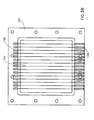
- a typical configuration of mesh electrodes 46, 52 and 54 is illustrated in Fig. 3A. These meshes are commercially available from Bopp AG, Bachnannweg 20, CH-8046 Zurich, Switzerland.
- FIG. 1B illustrates an alternative embodiment of the invention employing a different type of electron multiplier.
- the remainder of the apparatus is essentially identical to that described hereinabove in connection with Fig. 1A and therefore, similar elements thereof are indicated by identical reference numerals.
- an electron multiplier having a pre-amplification stage 60, a transfer stage 62 and an amplification stage 64 is employed.
- Typical voltages and gap separations at these stages for a gas pressure of 20 Torr are as follows:
- a preferred level of potential for the readout electrodes 36 is 0 V.
- the preferred levels of potential for the photocathode 20 and for the respective electrodes 65, 52 and 36 of each stage are:
- one of the mesh electrodes receives a selectably changeable voltage provided by a voltage source (not shown) via a switch 66, such as an HV 1000 Pulser, commercially available from DEI, 2301 Research Blvd., Suite 101, Fort Collins, Colorado, USA.
- a switch 66 such as an HV 1000 Pulser, commercially available from DEI, 2301 Research Blvd., Suite 101, Fort Collins, Colorado, USA.
- two voltage levels are provided.
- This arrangement enables mesh electrode 52 to act as a gate, having defined open and closed positions thereof, corresponding to the two voltage levels, thereby determining whether the electrons from the pre-amplification stage reach the amplification stage.
- Another function of the gate is to substantially prevent positive ions from drifting back to the photocathode and causing damage thereto.
- the gating function may be eliminated.
- a preferred level of potential for the readout electrodes 36 is 0.
- the preferred levels of potential for the photocathode 20 and for the respective electrodes 65, 52 and 36 of each stage are:
- FIG. 1 C illustrates yet another embodiment of X-ray detector constructed and operative in accordance with a preferred embodiment of the present invention.
- yet another type of electron multiplier is employed.
- the electrons emitted by the photocathode 20 initially pass through a transfer stage 70 and are subsequently amplified in a plurality of stages identical to that illustrated in Fig. 1A.
- insulative layer 72 typically formed of epoxy laminate and of thickness 200 microns.
- resistive layer 74 typically formed of graphite, or of a polymer paste, commercially available from Minico/Ashai Chemical of America, 50 North Harrison Ave., Congres, N.Y., USA.
- Resistive layer 74 has a typical resistivity of 10 MOhm/square. This structure allows operation of the photocathode at zero potential with the pad electrodes 36 at zero potential as well.
- Typical voltages and gap separations at these stages for a gas pressure of 20 Torr are as follows:
- a preferred level of potential for the photocathode 20 is 0 volts.
- the preferred levels of potential for the photocathode 20, for the electrodes 75, 76, 77 and 78 and for the resistive layer 74, respectively, are:
- FIG. 1D illustrates yet another embodiment of X-ray detector constructed and operative in accordance with a preferred embodiment of the present invention.
- yet another type of electron multiplier is employed, having a pre-amplification stage 80, first and second transfer stages 82 and 84, an amplification stage 86, and a third transfer stage 88.
- a mesh electrode 52 between the second transfer and the amplification stages which receives selectably changeable voltage via switch 66 and which consequently acts as a gate, as described hereinabove in connection with Fig. 1 B.
- Typical potentials across each stage and gap separations for each stage, for a gas pressure of 20 Torr are as follows:
- a preferred level of potential for the photocathode 20 is 0 volts.
- the preferred levels of potential for the photocathode 20, for the electrodes 90, 92, 52 and 94 and for resistive layer 74 are:
- an insulative layer 72 and a resistive layer 74 which may be identical to the respective layers 72 and 74 of Fig. 1 C.
- FIG. 1E illustrates yet another embodiment of X-ray detector constructed and operative in accordance with a preferred embodiment of the present invention.
- yet another type of electron multiplier is employed, having a first transfer stage 100, a preamplification stage 102, an amplification stage 104 and a second transfer stage 106.
- Typical potentials across each stage and gap separations for each stage, for a gas pressure of 20 Torr are as follows:
- a preferred level of potential for the electrodes 110 is 0 volts.
- the preferred levels of potential for the photocathode 20 and for the respective electrodes 101, 103, 105 and 110 of each stage are:
- one of the mesh electrodes receives a selectably changeable voltage from a voltage source (not shown) via a switch 107, such as an HV 1000 Pulser, commercially available from DEI, 2301 Research Blvd., Suite 101, Fort Collins, Colorado, USA.
- a switch 107 such as an HV 1000 Pulser, commercially available from DEI, 2301 Research Blvd., Suite 101, Fort Collins, Colorado, USA.
- two voltage levels are provided.
- This arrangement enables mesh electrode 101 to act as a gate, having defined open and closed positions thereof, corresponding to the two voltage levels.
- the function of the gate is to prevent positive ions from drifting back to the photocathode 20 and causing damage thereto, when the gate is closed.
- the gating function may be eliminated.
- a preferred level of potential for the electrodes 110 is 0 volts.
- the preferred levels of potential for the photocathode 20 and for the respective electrodes 101, 103, 105 and 110 of each stage are:
- Electrode array 34 of Fig. 1A is here replaced by a readout electrode assembly 108 shown in detail in Fig. 3D, typically comprising a first array of strip electrodes 110, typically in mutually parallel orientation, a generally planar insulating element 112 and a second array of strip electrodes 114, typically in mutually parallel orientation and being generally perpendicular to the orientation of strip electrodes 110.
- Electrode arrays 110 and 114 may take any suitable form such as a thin copper layer deposited on both sides of insulating element 112.
- the width of an electrode strip 110 is typically approximately 1-3 mm and the separation between adjacent strips is typically approximately 0.2 - 0.5 mm.
- the width of and separation between electrode strips 114 may be the same.
- the insulating element 112 may be formed of any suitable material such as epoxy laminate with a typical thickness of 200 microns.
- any suitable method may be employed to read out the information from the strip electrode arrays.
- the readout electronics 40 of previous embodiments is here replaced by readout electronics 116, such as described in V. Radeka and R.A. Boie, Nucl. Instrum. Methods 178 (1980) 543, the disclosure of which is incorporated herein by reference.
- Connectors 38 are here replaced by appropriate connectors (not shown) between strip electrode arrays 110 and 114, and readout electronics 116.
- the remainder of the apparatus is essentially identical to that described hereinabove in connection with Fig. 1A.
- FIG. 1F illustrates yet another embodiment of X-ray detector constructed and operative in accordance with a preferred embodiment of the present invention.
- yet another type of electron multiplier is employed, having a preamplification stage 120, first, second and third transfer stages 122, 124 and 126, and an amplification stage 128.
- Electrodes 130 and 132 receive selectably changeable voltages via switches 134 and 136 respectively.
- the voltages provided via switches 134 and 136 are preferably approximately -50 V and + 5 0 V, respectively.
- Typical potentials across each stage and gap separations for each stage, for a gas pressure of 20 Torr are as follows:
- a preferred level of potential for the electrode 110 is 0 volts.
- the preferred levels of potential for the photocathode 20 and for the respective electrodes 137, 130, 132, 138 and 110 of each stage are:
- any suitable method may be employed to read out the information from the strip electrode arrays.
- the readout electronics 40 of previous embodiments is here replaced by readout electronics 116, as in Fig. 1 E.
- Connectors 38 are here replaced by appropriate connectors (not shown) between strip electrode arrays 110 and 114, and readout electronics 116, again as in Fig. 1 E.
- the remainder of the apparatus is essentially identical to that described hereinabove in connection with Fig. 1A, and therefore, similar elements thereof are indicated by identical reference numerals.
- FIG. 1G illustrates yet another embodiment of X-ray detector constructed and operative in accordance with a preferred embodiment of the present invention.
- yet another type of electron multiplier is employed, having a preamplification stage 140, transfer stage 142, an amplification stage 144 and an insulative gap 145.
- the electrode 146 between the preamplification stage and transfer stage may be identical to the electrode 52 of Fig. 1A.
- electrode assemblies 148 and 150 defining the amplification stage 144 which are each preferably of the type illustrated in Fig. 3B. Unlike in the previous embodiments in which readout electrode assemblies are provided, in the present embodiment, electrode assemblies 148 and 150 are directly read by readout electronics 116.
- each electrode assembly 148 and each electrode assembly 150 comprises a generally planar insulating element 152, a plurality of wires 154 having a generally mutually parallel orientation and being soldered at each end to corresponding pluralities of soldering taps 156 and 158.
- the generally planar insulating element 152 may be formed of any suitable material such as epoxy laminate.
- the wires may be Tungsten gold-plated and may be of a diameter of approximately 20 - 100 microns. Suitable wires are commercially available from Lumalampen Corporation, Sweden. The spacing between wires may be approximately 1-2 mm.
- readout electronics 116 which may be identical to readout electronics 116 of Fig. 1E.
- Readout electronics 116 is connected to taps 158 by suitable connectors (not shown).
- the orientation of the parallel wires 154 of electrode assembly 148 is preferably generally perpendicular to the parallel wires 150.
- Typical potentials across each stage and gap separations for each stage, for a gas pressure of 20 Torr are as follows:
- a preferred level of potential for the electrode 150 is 0 volts.
- the preferred levels of potential for the photocathode 20 and for the respective electrodes 146, 148 and 150 of each stage are:
- FIG. 1 H illustrates yet another embodiment of X-ray detector constructed and operative in accordance with a preferred embodiment of the present invention.
- yet another type of electron multiplier is employed, having a first transfer stage 170, a preamplification stage 172, a second transfer stage 174, and first and second amplification stages 176 and 178, and an insulative gap 179.
- the electrodes 180 and 182 which define the preamplification stage 172 may be identical to the mesh electrode of Fig. 3A.
- electrode assemblies 184, 186 and 188, defining the first and second amplification stages which may be identical to electrode assemblies 148 and 150 of Fig. 1 G.
- Electrode assemblies 184, 186 and 188 may be arranged such that the respective wires thereof define any desired angle between them. For example, the wires of assemblies 184 and 186 may be parallel to one another, whereas the wires of assembly 188 may be perpendicular to the wires of the other two.
- Typical potentials across each stage and gap separations for each stage, for a gas pressure of 20 Torr are as follows:
- a preferred level of potential for the photocathode 20 is 0 volts.
- the preferred levels of potential for the photocathode 20 and the respective electrodes 180, 182, 184, 186 and 188 of each stage are:
- the readout electronics 116 of the present embodiment may be identical to readout electronics 116 of Fig. 1 E. Appropriate connectors (not shown) are provided between the electrode assemblies 184, 186 and 188, and readout electronics 116. It is appreciated that, due to this arrangement, a separate readout electrode assembly need not be provided.
- FIG. 11 illustrates yet another embodiment of X-ray detector constructed and operative in accordance with a preferred embodiment of the present invention.
- yet another type of electron multiplier is employed, having a preamplification stage 200, first, second and third transfer stages 202, 204 and 206 respectively, an amplification stage 208, and an insulative gap 209.
- the photocathode 20 is followed by three mesh electrodes 210, 212 and 214 which may be identical to electrode 52 of Fig. 1A, which is illustrated in detail in Fig. 3A.
- the three mesh electrodes are followed by three electrode assemblies 220, 222 and 224 which define the amplification stage 208 and which are each preferably of the type illustrated in Fig. 3B.
- preferred characteristics of the wires of the electrode assemblies are as follows:
- Electrodes 212 and 214 on both sides of the second transfer stage 204 act as gate electrodes in the present embodiment, receiving selectably changeable voltages via switches 226 and 228 respectively.
- the voltages provided via switches 226 and 228 are preferably approximately -50 V and + 50 V respectively.
- Typical potentials across each stage and gap separations for each stage, for a gas pressure of 20 Torr are as follows:
- a preferred level of potential for the photocathode 20 is 0 volts.
- the preferred levels of potential for the respective electrodes 210, 212, 214, 220, 222 and 224 of each stage are:
- the readout electronics 116 of the present embodiment may be identical to readout electronics 116 of Fig. 1 E. Appropriate connectors (not shown) are provided between the electrode assemblies and readout electronics 116. It is appreciated that, due to this arrangement, a separate readout electrode assembly need not be provided.
- Electrode assemblies 220, 222 and 224 may be arranged such that the wires thereof define any desired angle between them.
- the wires of assemblies 220 and 224 may be parallel to one another, whereas the wires of assembly 222 may be perpendicular to the wires of the other two.
- Figs. 2A-2B illustrate an X-ray photon detector combined with an optical sensor constructed and operative in accordance with preferred embodiments of the present invention.
- the X-ray detector 10 may comprise any suitable X-ray detector such as those shown and described hereinabove with reference to Figs. 1A - 11, but with the following exceptions:
- the mean number of photons emitted per avalanche electron was found to be 1.5.
- TEA gas mixtures were used, even higher mean values for the number of photons per avalanche electron, were found. Due to the above results, and since the light is emitted at the same location in space at which the charge is produced by the amplification process, localization and quantification of the light spot are equivalent to localization and quantification of the charge.
- Fig. 2A there is shown yet another type of electron multiplier having a preamplification stage 240, a transfer stage 242, and first and second amplification stages 244 and 246, and an insulative gap 243.
- the second amplification stage 246 acts as the main light amplifying element.
- the features of a typical light amplifying element are described in A. Breskin et al., "A highly efficient low pressure UV-RICH detector with optical avalanche recording," Nucl. Instrum. Methods A 273 (1988), p. 798 onwards, and in A. Breskin et al., "A Three Stage Gated UV Photon Gaseous Detector With Optical Imaging", Nucl. Instrum. Methods A 286 (1990) P. 251 onwards, the disclosures of which are incorporated herein by reference.
- the electrodes 245, 247, 248 and 249 defining the four stages referenced hereinabove, with the exception of photocathode 20, may be identical to electrode 52 of Fig. 1A, which is illustrated in detail in Fig. 3A.
- Typical potentials across each stage and gap separations for each stage, for a gas pressure of 40 Torr are as follows:
- a preferred level of potential for the photocathode 20 is 0 volts.
- the preferred levels of potential for the respective electrodes 245, 247, 248 and 249 of each stage are:
- the optical system 234 recording the information from detector 10 comprises a UV transparent lens 250, such as a FLECTAN 75 Q, commercially available from NYE Optical Company, Spring valley, CA, USA.
- the image is transferred to a position sensitive optical element 252, such as an array of position sensitive photomultipliers, such as an XP 4702 photomultiplier with a sapphire window, commercially available from Phillips.
- the information from optical element 252 is received by readout electronics 254, such as that described by G. Comby et al., Nucl. Instrum. Methods A243 (1986), p. 165-172, the disclosure of which is incorporated herein by reference.
- FIG. 2B there is shown yet another type of electron multiplier having a first transfer stage 260, a preamplification stage 262, a second transfer stage 264, an amplification stage 266 which acts as the main light amplifying element, and an insulative gap 265.
- a first transfer stage 260 a preamplification stage 262
- a second transfer stage 264 amplification stage 266 which acts as the main light amplifying element
- the electrodes 267, 268, 269 and 271 defining the four stages referenced hereinabove, with the exception of photocathode 20, may be identical to electrode 52 of Fig. 1A, which is illustrated in detail in Fig. 3A.
- Typical potentials across each stage and gap separations for each stage, for a gas pressure of 40 Torr are as follows:
- a preferred level of potential for the photocathode 20 is 0 volts.
- the preferred levels of potential for the respective electrodes 267, 268, 269 and 271 of each stage are:
- the optical system 236 recording the information from detector 10 comprises an optical taper 270, such as the custom-made taper commercially available from Schott Fibre Optics Inc., Southbridge, MA, USA, which is coupled to the optical window 238 via a wavelength shifter 272, such as p-terphenyl.
- the optical taper 270 is coupled to an image intensifier assembly 274, such as a BV 2562QX light amplifier coupled to a BV 1833 EG11 light amplifier, both commercially available from Proxitronic of Bensheim, W. Germany.
- Image intensifier 274 is coupled to a position sensitive optical element 276, such as a CCD camera, typically a 7864FO, commercially available from Thomson - France, which is read out by readout electronics 278, such as Thomson Driving Electronics Kit model TH 79K64 coupled to frame grabber and digitizer DT28581, commercially available from Data Translation of Marlboro, MA, USA.
- the digitizer output may be supplied for frame analysis to a computer such as a PC/AT, used in conjunction with suitable software such as DT-IRIS, commercially available from Data Translation, Marlboro, MA, USA.
- the position sensitive optical element 276 and the readout electronics 278 may be replaced by the position sensitive optical element 252 and the readout electronics 254, respectively, of Fig. 2A.
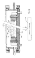
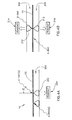
- Figs. 4A and 4B illustrate X-ray detectors in which the photocathode is planar and is capable of receiving X-ray radiation impinging on either or both sides thereof, constructed and operative in accordance with alternative embodiments of the present invention.
- the X-ray photons may impinge upon the photocathode 20 of the detector 10 at any desired angle alpha.
- the angle alpha will be relatively large, i.e. in the range of approximately 80 to 90 degrees from the perpendicular, to enhance the detection efficiency.
- X-ray photons may impinge upon the photocathode 20, associated with electron multiplier 300 disposed downstream thereof, from either the upstream side or the downstream side thereof.
- X-ray photon beam (a) is shown impinging upon the upstream side of the photocathode, whereas the X-ray photon beam (b) is shown impinging upon the downstream side thereof.
- Electron multiplier 300 creates an electron avalanche 302, read out by a readout system 304, as shown.
- Electron multipliers 306 and 308 may be provided on both respective sides of photocathode 20, which in this embodiment comprises a double side photocathode 20 such as the photocathode assemblies shown in Figs. 6A and 6G.
- Electron multipliers 306 and 308 each create an electron avalanche, referenced 310 and 312 respectively, amplifying electrons from the photocathode 20.
- Electron multipliers 306 and 308 are preferably read out separately by readout systems 314 and 316, respectively, as shown.
- the X-ray photons may impinge upon the photocathode 20 from either side thereof.
- Assembly 330 comprises a low-pressure gas filled enclosure 332 including an entrance window 334, typically formed of polypropylene supported on a frame (not shown), similar to the window 14 and frame 16 shown and described with reference to Fig. 1A.
- the assembly 330 comprises a plurality of stacked X-ray detector modules 336, rather than a single such module as in the embodiments of Fig. 1A-11.
- Each module may comprise an electron multiplier identical to the various embodiments thereof disclosed with reference to Figs. 1A-11.
- the modules are arranged in a generally mutually parallel orientation which is at an angle beta of typically 1 to 10 degrees from the X-ray beam impingement direction 338. It is noted that individual windows need not be provided for each individual module 336. Rather, the entire enclosure 332 is a single gas filled enclosure.
- a photocathode comprising a metal foil 350 which may be formed of any suitable conducting material such as tantalum, gold, platinum, aluminum, or tungsten, of a thickness depending on the energy of impinging photons.
- a gold layer 350 and an X-ray energy of 10 KeV a typical thickness is approximately 5 microns.
- a typical thickness is approximately 15 microns.
- Fig. 6B shows a photocathode assembly comprising a thin semiconductive or metal photocathode layer 352 deposited upon an insulative support foil layer 354.
- Thin layer 352 may be formed of any suitable semiconductive or conducting material, such as Cul or gold, of a suitable thickness which depends on the energy of the impinging photons. For example, for a Cul layer 352 and an X-ray energy of 10 KeV, a typical thickness is approximately 1 micron. If the X-ray energy is 80 KeV, a typical thickness is approximately 30 microns.
- the insulative support foil layer 354 may be formed of any suitable electrically insulative, low X-ray absorbing material such as polypropylene, Parylene M, Kapton, Mylar, Aclar or Nylon, of suitable thickness. For example, for an X-ray energy of 10 KeV, a typical thickness is in the range of 5-50 microns.
- Fig. 6C shows a photocathode assembly comprising a nonconductive (insulating or semi-conducting) photocathode layer 356 deposited upon a thin metal support layer 358.
- Photocathode layer 356 may be formed of any suitable nonconductive material such as Csl or Cul of a suitable thickness which depends on the energy of impinging photons. For example, for a Csl photocathode layer 356 and an X-ray energy of 10 KeV, a typical thickness is approximately 1.5 microns. For an X-ray energy of 80 KeV, a typical thickness is approximately 45 microns.
- the support layer 358 may be formed of any suitable metal such as aluminum, gold or copper, of suitable thickness. For example, for a gold layer 358 and an X-ray energy of 10 KeV, a typical thickness is 5-10 microns.
- Fig. 6D shows a photocathode assembly comprising a thin insulative support layer 360 followed by a thin conductive layer 362 and a nonconductive photocathode layer 364.
- Support layer 360 may be identical to support layer 354 of Fig. 6B.
- Conductive layer 362 may be formed of any suitable material such as aluminum, gold or Nichrome of suitable thickness. For example, a gold layer 362 is typically approximately 1 micron thick.
- Photocathode layer 364 may be identical to photocathode layer 356 of Fig. 6C.
- Fig. 6E shows a photocathode assembly comprising a metal support layer 366 followed by a low density nonconductive photocathode layer 368.
- Metal support layer 366 may be identical to support layer 358 of Fig. 6C.
- Photocathode layer 368 may be formed of a layer of fluffy (low density) Csl, typically with a density of approximately 1-3% of the bulk density of Csl and being of a suitable thickness. For example, for an X-ray energy of 5 KeV, a typical thickness is in the range of 1000 micrograms/cm 2. Details of a preferred material suitable for photocathode layer 368 are provided in C. Chianelli et al., Nucl. Instrum. Methods A 273 (1988) p.
- Fig. 6F shows a photocathode assembly comprising a support layer 370 followed by a nonconductive photocathode layer 372 and a thin metal layer 374.
- Support layer 370 may be identical to support layer 358 of Fig. 6C.
- the photocathode layer 372 may be identical to photocathode layer 356 of Fig. 6C.
- the thin metal layer 374 may be formed of any suitable material such as Nichrome, Aluminum, or Gold having a thickness of 0.05 - 1 micron.
- Fig. 6G shows a photocathode assembly 376 corresponding to the photocathode assembly of Fig. 6D but being double-sided. It is appreciated that any of the photocathode assemblies of Figs. 6B-6F may similarly be provided in double-sided form.
- Photocathode assembly 376 comprises a thin insulative support layer 380 sandwiched between a first thin conductive layer 382 followed by a nonconductive photocathode
- Ultrasoft X-rays are detected by counting single electron clusters induced in the gas.
- X-ray induced UV-photons in Gas Scintillation Chambers are read out with wire chambers coupled to CsI photocathodes.
- X-rays converted in foil-electrodes are imaged by fast multistep avalanche electron multipliers.
- Thin insulative support layer 380 may be identical to support layer 360 of Fig. 6D.
- First and second thin conductive layers 382 and 386 may be identical to conductive layer 362 of Fig. 6D.
- Photocathode layers 384 and 388 may be identical to photocathode layer 364 of Fig. 6D.
- the photocathode assembly in Fig. 6A is particularly useful in high energy X-ray applications (in the range of approximately 50 - 500 KeV).
- the photocathode assemblies in Figs. 6B-6D and 6F-6G are particularly useful in the low and medium energy range (approximately 6 - 50 KeV).
- the photocathode assembly in Fig. 6E is particularly useful in the very low energy range (approximately 0.1 - 6 KeV).
- the performance of the detector including the photocathode of Fig. 6A is seen in Fig. 7A.
- the performance of the detector including the photocathode of Fig. 6C is seen in Fig. 7B.
- the quantum efficiency of the photocathode of Fig. 6C considerably exceeds the quantum efficiency of the photocathode of Fig. 6A.
- timing response of an X-ray detector including the photocathode of Fig. 6C was measured using a UV radiation source rather than an X ray radiation source.
- the timing was found to be approximately 4 nanoseconds for a single electron event and less than one nanosecond for a multielectron event. It is believed that this result is approximately 100 times superior to results obtained using state of the art X ray detectors. For example, fast scintillators have timing of a few microseconds.
- the detection resolution was found to be of the order of 0.2 mm.
- a preferred embodiment of X-ray detector employed for medical purposes is one which is sensitive to a relatively small amount of radiation, such as the embodiments of Fig. 4B or 5. It is believed to be most preferable to employ an embodiment of X-ray detector which combines the double-sided characteristic of the embodiment of Fig. 4B with the relatively small angle between the photocathode surface and the direction of radiation provided in the embodiment of Fig. 5.
- the disclosure of the present invention is also believed to have industrial applications in monitoring and controlling dynamic industrial processes such as lubrication of mechanical parts and flows of fluids through mechanical systems.
- the disclosure of the present invention is also believed to be applicable to screening of static objects such as screening of luggage at air facilities to detect weapons and narcotics.
- a particular feature of the apparatus and methods of X-ray detection disclosed herein is the relatively high detection resolution achieved thereby. This feature is particularly important in industrial and security applications.
- Photosensitive LPMSC's 5,6 efficiently detect UV-photons in Cerenkov Ring Imaging detectors 7) (RICH) and UV-photons emitted from BaF 2 scintillation in application to particle physic 8) and medicine 9) .
- Single electron cluster counting methods are developed for particle identification by their specific ionization 10) and for soft X-ray spectroscopy.
- Primary Ionization Cluster Counting is performed by coupling a multistep electron multiplier to a large low-pressure, low-field, conversion and drift volume, in which particles or soft X-rays induce trails of primary charges.
- PICC Primary Ionization Cluster Counting
- ultra-soft X-rays 0.1-1 keV
- primary charges are efficiently separated in space and time. They are individually multiplied and counted and their number is proportional to the X-ray energy. The resulting energy resolution competes with that of gas scintillation counters.
- the quantum efficiency (QE) of the UV-detector is of the order of 10%.
- the X-rays are localized with an accuracy of 2 mm. The device is fast and allows background reduction by pulse-shape analysis.
- High-resolution detection of soft-X-rays is required in materials science for surface analysis with electron microprobes.
- this domain in parallel to the conventional surface image, one detects characteristic X-rays emitted by the impact of the electron beam with the analyzed sample surface.
- This allows the correlation of topography with chemical composition.
- the energy range of 0.1-1 keV corresponding to characteristic X-rays of light elements such as B, C, O, N etc.
- the standard technique employs cryogenic Si-Li detectors separated from the high-vacuum chamber of the analyzed sample by a thin Be window. This window, usually about 10 ⁇ m thick, introduces severe limitations since it absorbs most of the characteristic radiation of elements up to Na. Room temperature Si-Li detectors, operating without Be windows, are ineffective below 400 eV, due to poor signal-to-noise ratio.
- the primary ionization cluster counting (PICC) at low gas pressures may well be a suitable method for the spectroscopy of ultrasoft X-rays. It is well known that the energy resolution of a gaseous detector depends on several factors and to first order it may be written as where N P is the mean number of primary ion pairs.
- the first term contains the Fano factor F which describes the statistical fluctuations in the primary ionization process.
- a counting gas in the present method is somewhat easier than in GSC's, where highly purified Xe or its mixtures with other noble gases are employed.
- the present method does not require complex purification systems as is the case with GSC's.
- the detector of circular geometry and active area of 50 cm 2 , has a 20 cm long conversion region followed by a double-stage, parallel grid, amplification structure. All the electrodes are made of stainless steel mesh, 50 ⁇ m diameter and 500 ⁇ m cell size. The mesh is supported by epoxy resin frames. The conversion volume is made of a Delrin cylinder covered on the inside with a Kapton layer with etched copper strips. The strips are 3 mm wide and 5 mm apart. A resistor chain provides a. constant potential gradient.
- the X-ray source is housed in a vacuum cell, separated from the detector by a 20 mm diameter, 60 ⁇ g/cm 2 thick, polypropylene foil, placed close to the end-cup mesh of the drift cell.
- a commercial 244 Cm ⁇ -induced X-ray source with changeable targets 18) a commercial 244 Cm ⁇ -induced X-ray source with changeable targets 18) .
- Soft X-rays which enter the conversion volume produce a trail of primary charges. For example, 279 eV C-K induced primary electrons typically extend over 1 mm at a gas pressure of 10 Torr. The electrons drift at low-field of about 0.5 V/cm ⁇ Torr, towards the first 3 mm wide parallel-plate amplification gap.
- Each primary electron is independently amplified.
- a fraction of the preamplified avalanche is transferred through a low-field transfer region to a second parallel grid amplification element which provides the signals for electron counting and, as an option, for localization. These signals are shaped by a fast amplifier and fed into a digitizer.
- Each event is stored in a PC computer as an array of 2K elements, 10 bits each.
- Fig. 2 gives examples of events induced by C-K 279 eV photons in 8 Torr of a C 2 H 6 / Ar (80/20) gas mixture.
- the X-ray photons are absorbed in the first few cm of the conversion volume and produce on the average 10.7 primary charges.
- the primary electron swarm expands, due to the diffusion, over 1-2 cm (2-4 psec).
- the individual electron signals have a full width of about 50 ns.
- Cosmic events have different cluster-density and total time spread and can be easily discriminated against.
- the primary cluster counting can be performed with fast discriminators followed by proper pulse integrators 10 ).
- an analog pulse digitization followed by a software- based cluster counting, is more adequate for the systematic study of the PICC method.
- We used the correlation method 19,20) demonstrated in fig. 3, which provides automatic peak counting by scanning the data with a "search-function" of known shape and recording the correlation between the data and the "search-function". This method is quite sensitive and is capable of recognizing peaks which are not fully separated, as is seen in fig. 3.
- FIG. 5 Based on a given X-ray photon energy, mean ionization energy and Fano factor, we generate an "input distribution" of primary charges (Fig. 5a). Using a random choice process we define the number of injected primary charges for each event. We use known diffusion, drift length, single electron avalanche size distribution and signal rise/fall times to generate the "detected pulse trails" (Fig. 5b). We analyze each event with the correlation method 19,20) (Fig. 5c) and generate the "measured" distribution of counted primary electrons (Fig. 5d).
- Rough localization of the X-ray photons may be obtained with the present detector by reading out electric or optical signals induced during the amplification process at the second multiplication stage. Since the detected charge contains N c clusters extending typically over 15-20 mm (FWHM), a localization accuracy of the order of 20/ ⁇ N c mm is expected, i.e. about 7 mm (FWHM) for 279 eV photons, and of about 4 mm (FWHM) for 1 keV photons.
- GSC Gas Scintillator Counters
- Fig. 6 the Solid Photocathode Avalanche Chamber (SPAC) coupled to a GSC through a CaF 2 window is shown.
- the GSC was designed for X-ray detection in the energy range of 15-150 keV.
- the system offers the possibility of identifying X-ray interactions, in a high Gamma background, by means of K-fluorescence gating 30) , pulse-shape analysis and a three-dimensional imaging capability 21 ).
- the GSC is filled with continuously purified- xe at pressures up to 10 bar.
- X-ray photons enter the detector through a 0.2 mm thick aluminum window, 50 mm in diameter, and interact in a 60 mm deep conversion-drift gap. Primary scintillation is produced at the interaction point.
- the inside of the cell is coated with UV-reflective paint.
- the primary electron cloud drifts in a parallel field towards a 3 mm wide secondary scintillation gap.
- An electric field of -14 kV/cm across the secondary scintillation gap yields about 500 photons per initial electron at a pressure of 4.5 bar.
- the localization of the avalanche is made by charge division, using cathode-induced signals. Anode signals are used for timing, pulse shape analysis and energy measurement.
- the SPAC is typically operated at 5-20 Torr of CH 4 , which has low self-absorption of UV light.
- the multistep amplification mode provides high gain, essential for efficient simultaneous detection of primary and secondary scintillation light. The primary scintillation light is detected with 65% efficiency for 60 keV X-ray photons. More details on the detector structure, operation and readout electronics, are given elsewhere 29 ).
- Fig. 7 we present an energy spectrum of an 241 Am source obtained with the GSC+SPAC detector.
- the energy resolution of this device is dominated by several factors: the statistics of the primary electrons in the Xe gas, characterized by the Fano factor, the UV-light collection and conversion efficiency and the statistical fluctuations of the photoelectron amplification process.
- the contributions due to Fano statistics and to the light collection and amplification in the SPAC are 1.8% and 3.1% FWHM, respectively.
- the measured value of 4.1% (FWHM) at 60 keV is in good agreement with a total expected resolution of 3.7% (for more details see ref. 29).
- the three dimensional conversion point of the X-ray photon is derived from the center of the avalanche in the SPAC plane and the time elapsed between the primary and secondary scintillation pulses.
- the accuracy of localization is limited by the finite range of the photo-electron, which depends on the Xe pressure, by the distribution of UV-photons detected at the photocathode and by the statistical fluctuations of the amplification process in the SPAC.
- the resolution in the third dimension is also a result of several factors - the finite size of the primary ionization cloud, the diffusion along the drift over 6 cm and the finite width of the secondary scintillation light pulse caused by the diffusion and by the size of the scintillation gap itself. In the present detector the resolution in this dimension is about 3 mm FWHM.
- the timing properties of the SPAC were studied with triggerable UV light sources of two types: a discharge H 2 lamp and a BaF 2 scintillator coupled to a 22Na source.
- the H 2 lamp can yield a high UV-photon flux in each discharge pulse.
- the time response of the SPAC to a multiple-photon light pulse (> 100 photons) is shown in Fig. 9; the resolution is ⁇ 350 ps (FWHM).
- the time response of the SPAC to a pulse.of ⁇ 8 photoelectrons (collimated H 2 lamp), which is the typical size of a primary scintillation pulse for 60 keV X-ray in our GSC-SPAC detector (the ratio of secondary-to-primary light is of ⁇ 10 3 ), is shown in Fig. 10.
- the resolution is 650 ps FWHM.
- the time response of the SPAC was measured with a 22 Na source and two BaF 2 crystals in a back-to-back geometry. One crystal was mounted on the SPAC and the other was read by a Philips P2020Q photomultiplier (PM), providing a time zero signal. In this configuration mostly single photoelectrons are associated with each trigger of the PM.
- the time resolution measured in this configuration is 4.5 ns (FWHM) with 10 Torr CH 4 and 4.2 ns (FWHM) with 38 Torr C 2 H 6 , for single UV photons.
- the quantum efficiency of the SPAC to Xe (170 nm) and Kr (150 nm) UV radiation was measured with a spherical anode gas scintillation source, described in Ref. 28.
- the absolute QE of the Csl photoca.thode was calculated by calibrating the source photon flux, using two different methods: a) the SPAC was replaced by a Hamamatsu PM type R1460, having a LiF window and CsSb-PC. The producer supplies absolute gain curves and QE data over the range of 120-300 nm. b) A small ionization cell filled with TMAE vapor at controlled temperature was mounted directly on the source.
- the UV light photoionizes the TMAE in the volume between the cathode meshes of the TMAE cell (17.6 mm wide) and induces measurable photo-current on the anode wires and cathodes.
- the source intensity was derived from the known photon mean free path 5) and the QE 31) of TMAE.
- a reference photomultiplier continuously monitored the source relative intensity. More details of these measurements will be given in ref. 32.
- the CsI layer was prepared by vacuum evaporation onto a polished metallic surface, cleaned by glow discharge prior to evaporation.
- the photocathodes were installed in the detector immediately after evaporation. Their contact with air was between 1-2 min, which supposedly has only a minor effect on the QE 28) .
- the detector was either immediately evacuated to a vacuum of the order of 10- 2 Torr, or flushed with CH 4 during hours or days, prior to operation. There was no noticeable change in the QE during the pumping or flushing process, as opposed to the observation of the authors of ref. 33.
- Several photocathode substrates were tested: copper, stainless steel, aluminized copper and aluminized stainless steel.
- the QE was found to be insensitive to the substrate material, although the aging of the photocathode was dependent on the quality and type of the surface 32) .
- the following values of the absolute quantum efficiency (QE) were measured with a SPAC, operating at 20 Torr CH 4 and with a 1500 nm thick CsI photocathode:
- Fig. 11 The dependence of the quantum efficiency of the SPAC on the CH 4 operation pressure is shown in Fig. 11. There is a drop of about 20% in QE for atmospheric pressure relative to 20 Torr of CH 4 .
- Fig. 12 shows the dependence of the QE on photocathode thickness. Only a small vacation is noticeable with a peak around 600 nm.
- Fig. 13 shows the decay of the QE due to exposure of the photocathode to air. It is important to note that the decay time constant is of the order of an hour. However, since our mounting procedure involves an exposure to air of about 1-2 min, it may well be that some damage, of unknown extent, has already been initiated. The aging of the CsI photocathode induced by the UV flux and the feedback of positive ions was studied by irradiating the SPAC through its CaF 2 window.
- Xe UV-light source and a low-pressure Hg/Ar lamp (ORIEL) were used.
- the Hg/Ar lamp can provide extremely high photon flux, of more than 10 13 photons/mm 2 .s.
- the SPAC was operated in different modes in order to control the flow of positive ions back-streaming onto the photocathode. Some examples are given here and more details can be found in references 29 and 32.
- Fig. 14 shows the decay of the QE under an illumination of 10 8 photons/mm 2 . s.
- the total detector gain in the two curves is constant but is differently distributed between the two amplification stages. As expected, a higher gain in the preamplification stage induces a faster decay of the photocathode, due to the positive ions feedback.
- curves a) and b) demonstrate the effect of the gas pressure: for the same total gain a slower decay occurs at higher pressure. This is interpreted to be due to the lower velocity of molecular radicals in the gas. Comparing b) and c) in the same figure we see that an increase by a factor of 100 in photon flux causes more damage than an equal increase in gain of the preamplification stage. From the QE decay data at different operation conditions we can extract a typical "life-time" for the photocathode. For example, at 20 Torr CH 4 , with a gain of 100 in the preamplification stage (Fig.
- the photocathode decays to 50% of its initial value after a total charge, measured at the second stage, of 0.6 mC, equivalent to a dose of 10" incident photons/mm 2 .
- a total charge measured at the second stage, of 0.6 mC
- each 60 keV X-ray photon induces about 10 photons/mm 2 . Therefore an effective life-time of the photocathode is associated with a dose of about 10 12 X-rays under these operative conditions.
- the last application presented here is a fast X-ray imaging detector based on a solid foil convertor coupled to a LPMSC.
- This device may be used over a broad range of X-ray energies by a proper choice of the photocathode material and thickness.
- Many applications can be envisioned such as X-ray microscopy, surface analysis with electron microbeams, X-ray diffraction in protein crystallography using intense Synchrotron Radiation Sources, industrial radiography for safety and quality controls, study of time-resolved phenomena such as proteins in muscles or plasma diagnostics involved in thenno-naclear fusion and X-ray detection in Transition Radiation detectors.
- the obvious advantages of a solid photocathode, as compared to gaseous conversion, are the production of parallax-free images and a fast response.
- the low-pressure operation mode of the electron multiplier enables a high rate capability due to the low-charge density in the avalanche and fast ions removal.
- Fig. 16 shows the structure of the detector. It consists of several, 80 mm diameter, mesh electrodes mounted in a vacuum vessel.
- All the mesh frames and spacers are made of G-10 epoxy resin.
- a thin window made of 100 ⁇ m Kapton was used.
- the photocathode is made of a thin layer (400-2000 A) of CsI, vacuum deposited on commercial 1.5 ⁇ m thick aluminized mylar.
- the metallic substrate is important for providing the potential to this electrode.
- the electrons emitted from the photocathode are immediately amplified in a 3 mm wide parallel gap, transferred and further amplified in a second parallel gap structure.
- a different configuration in which the electrons emitted from the photocathode are first collected in a 3 mm drift region and only then transferred and amplified, was also tested.
- Fig. 17 shows the amplification curve of a single gap with DME at 20 Tnrr when operated with UV photons.
- the detector was tested with 6 keV X-rays from 55 Fe source.
- Fig. 18 shows the pulseheight spectrum obtained from the photocathode with and without the CsI layer. An electron yield due to the Al layer is evident in a), and an enhancement of the yield due to the CsI layer is shown in b). Under the same conditions a spectrum induced by UV photons is given in c). The photocathode obviously yields several electrons for each absorbed X-ray photon.
- the current from the last anode of the detector is shown in Fig. 19 as function of the voltage on this anode; a plateau extends over a few hundred volts.
- the plateau region was used for the measurement of the QE of the CsI in our gaseous electron multiplier.
- the CsI layer of 480 ⁇ yielded a QE of 0.92%, for 90 day incidence angle of an X-ray beam.
- the absorption fraction of X-rays in this CsI layer is 1%. This demonstrates the high efficiency of the device for detecting the secondary electrons.
- a thicker CsI layer has to be used.
- a promising possibility is the use of a grazing incidence angle geometry (Fig. 20) which provides a larger absorption length for X-rays without increasing the actual thickness which may reduce electron extraction 37).
- a large-surface imaging UV-photon detector combining a CsI photocathode and a x wire chamber, provides an efficient readout for GSC's, with fast timing and good localization properties for mid-energy X-rays.
- the CsI photocathode has a quantum efficiency of 10% at 170 nm. Its stability was systematically investigated.
- Our fast gaseous UV-imaging photomultiplier may be an ideal tool for the readout of solid scintillators (BaF 2 , KMgF 3 38) and others) in particle physics, medical or industrial positron tomography and gamma radiography. Single photon impact can be localized with an accuracy of 0.2 mm (FWHM) 25 .
- Other possible applications are UV-astronomy, plasma diagnostics and Cerenkov ring imaging. Different photocathodes, also for the visible spectrum, will be investigated for this purpose.
- a fast high rate imaging X-ray detector based on a conversion foil coupled to a multistep avalanche multiplier, is being studied. It should provide a parallax-free high accuracy localization of X-rays over a broad energy range, with subnanosecond time resolution (Sect. 3.1).
- the efficient secondary-electron detection provides high counting efficiencies for-Xrray quanta converted in the photocathode foils.
- Systems combining several layers of detectors based on this principle are suited for applications in medical and industrial radiography and for high rate X-ray diffraction experiments at Synchroton Radiation Accelerators. Such detectors enable the study of fast dynamical processes.
Landscapes
- Measurement Of Radiation (AREA)
Applications Claiming Priority (2)
| Application Number | Priority Date | Filing Date | Title |
|---|---|---|---|
| IL93969 | 1990-04-01 | ||
| IL93969A IL93969A (en) | 1990-04-01 | 1990-04-01 | Ultrafast x-ray imaging detector |
Publications (2)
| Publication Number | Publication Date |
|---|---|
| EP0450571A2 true EP0450571A2 (fr) | 1991-10-09 |
| EP0450571A3 EP0450571A3 (en) | 1992-02-19 |
Family
ID=11061075
Family Applications (1)
| Application Number | Title | Priority Date | Filing Date |
|---|---|---|---|
| EP19910105189 Ceased EP0450571A3 (en) | 1990-04-01 | 1991-04-02 | Ultrafast x-ray imaging detector |
Country Status (3)
| Country | Link |
|---|---|
| US (1) | US5192861A (fr) |
| EP (1) | EP0450571A3 (fr) |
| IL (1) | IL93969A (fr) |
Cited By (6)
| Publication number | Priority date | Publication date | Assignee | Title |
|---|---|---|---|---|
| US5355391A (en) * | 1992-03-06 | 1994-10-11 | Rambus, Inc. | High speed bus system |
| WO1999021211A1 (fr) * | 1997-10-22 | 1999-04-29 | European Organization For Nuclear Research | Detecteur de rayonnements a tres haute performance et imageur a rayons x planispherique sans parallaxe |
| WO2001094979A1 (fr) * | 2000-06-05 | 2001-12-13 | Xcounter Ab | Appareil et procede de detection de rayons |
| WO2001094981A1 (fr) * | 2000-06-05 | 2001-12-13 | Xcounter Ab | Dispositif et procede de detection des rayonnements |
| WO2003054902A1 (fr) * | 2001-12-11 | 2003-07-03 | Lightlab Ab | Systeme et procede d'emission de lumiere |
| WO2005006017A1 (fr) * | 2003-07-02 | 2005-01-20 | European Organisation For Nuclear Research - Cern | Detecteur multifonctionnel destine a mesurer des caracteristiques d'un faisceau de particules ou de rayonnement |
Families Citing this family (22)
| Publication number | Priority date | Publication date | Assignee | Title |
|---|---|---|---|---|
| US5285061A (en) * | 1992-08-28 | 1994-02-08 | Csl Opto-Electronics Corp. | X-ray photocathode for a real time x-ray image intensifier |
| US5308987A (en) * | 1993-02-01 | 1994-05-03 | The United States Of America As Represented By The United States Department Of Energy | Microgap x-ray detector |
| US5491331A (en) * | 1994-04-25 | 1996-02-13 | Pilot Industries, Inc. | Soft x-ray imaging device |
| FR2723256B1 (fr) * | 1994-07-29 | 1996-08-30 | Thomson Tubes Electroniques | Procede d'utilisation d'un tube intensificateur d'image radiologique et circuit pour la mise en oeuvre de ce procede |
| DE69613131T2 (de) | 1996-12-04 | 2001-11-22 | Agfa-Gevaert N.V., Mortsel | Röntgenbilddetektor und Bildauslesevorrichtung |
| US6429578B1 (en) * | 1999-01-26 | 2002-08-06 | Mats Danielsson | Diagnostic and therapeutic detector system for imaging with low and high energy X-ray and electrons |
| US6326654B1 (en) | 1999-02-05 | 2001-12-04 | The United States Of America As Represented By The Secretary Of The Air Force | Hybrid ultraviolet detector |
| SE514471C2 (sv) * | 1999-04-30 | 2001-02-26 | Xcounter Ab | Röntgendetektorenhet med omvandlare av fast typ |
| JP2001135267A (ja) * | 1999-09-08 | 2001-05-18 | Siemens Ag | 輻射変換器 |
| US6365902B1 (en) * | 1999-11-19 | 2002-04-02 | Xcounter Ab | Radiation detector, an apparatus for use in radiography and a method for detecting ionizing radiation |
| GB2359187A (en) * | 2000-02-11 | 2001-08-15 | Kindbrisk Ltd | Device and method for two-dimensional detection of particles or electromagnetic radiation |
| US6891166B2 (en) * | 2002-07-02 | 2005-05-10 | Ray Therapy Imaging Ab | Multi-layered radiation converter |
| US6847042B2 (en) * | 2003-06-19 | 2005-01-25 | Ge Medical Systems Global Technology Co., Llc | Centroid apparatus and method for sub-pixel X-ray image resolution |
| US7564039B1 (en) * | 2004-06-17 | 2009-07-21 | Integrated Sensors, Llc | Dual substrate plasma panel based ionizing radiation detector |
| KR100716495B1 (ko) * | 2005-11-23 | 2007-05-10 | 창원대학교 산학협력단 | 기체전자증폭기를 이용한 디지털 영상 광 검출장치 |
| US7667399B2 (en) * | 2007-04-26 | 2010-02-23 | The United States Of America As Represented By The Secretary Of The Navy | Large area hybrid photomultiplier tube |
| GB2475063A (en) * | 2009-11-04 | 2011-05-11 | Univ Leicester | Charge detector for photons or particles. |
| TWI449284B (zh) * | 2011-06-27 | 2014-08-11 | Univ Nat Formosa | Light amplification device |
| US9837238B2 (en) | 2015-08-26 | 2017-12-05 | National Security Technologies, Llc | Photocathode |
| CN107091851B (zh) * | 2017-07-03 | 2024-06-11 | 同方威视技术股份有限公司 | 大面积x射线气体探测器 |
| CN110571114B (zh) * | 2019-09-04 | 2021-08-13 | 中国科学技术大学 | 一种气体x射线像增强器 |
| CN110600358B (zh) * | 2019-09-04 | 2021-12-14 | 中国科学技术大学 | 气体电子倍增器、气体光电倍增管及气体x射线像增强器 |
Family Cites Families (7)
| Publication number | Priority date | Publication date | Assignee | Title |
|---|---|---|---|---|
| US3710125A (en) * | 1970-04-29 | 1973-01-09 | Univ Northwestern | Secondary emission enhancer for an x-ray image intensifier |
| GB1455012A (en) * | 1973-06-04 | 1976-11-10 | Agfa Gevaert | Method and apparatus for producing electrostatic charge patterns |
| FR2445613A1 (fr) * | 1978-12-29 | 1980-07-25 | Thomson Csf | Tube intensificateur d'image radiologique et chaine de radiologie incorporant un tel tube |
| US4376892A (en) * | 1980-10-16 | 1983-03-15 | Agence Nationale De Valorisation De La Recherche (Anvar) | Detection and imaging of the spatial distribution of visible or ultraviolet photons |
| US4395636A (en) * | 1980-12-24 | 1983-07-26 | Regents Of The University Of California | Radiation imaging apparatus |
| DE3638893A1 (de) * | 1986-11-14 | 1988-05-26 | Max Planck Gesellschaft | Positionsempfindlicher strahlungsdetektor |
| IL88299A (en) * | 1988-11-07 | 1992-01-15 | Yeda Res & Dev | Apparatus for radiographic imaging |
-
1990
- 1990-04-01 IL IL93969A patent/IL93969A/xx not_active IP Right Cessation
-
1991
- 1991-03-27 US US07/675,652 patent/US5192861A/en not_active Expired - Fee Related
- 1991-04-02 EP EP19910105189 patent/EP0450571A3/en not_active Ceased
Non-Patent Citations (12)
| Title |
|---|
| "proportional chamber for a digital radiographic installation", NUCLEAR INSTRUMENTS AND METHODS IN PHYSICS RESEARCH, vol. A283, 1989, pages 431 - 435 |
| A. BRESKIN ET AL.: "A highly efficient low-pressure UV-RICH detector with optical avalanche recording", NUCL. INSTRUM. METHODS, vol. A273, 1988, pages 798 |
| A. BRESKIN ET AL.: "In beam performance of a low-pressure UV-RICH detector", IEEE TRANS. NUCL. SCI., vol. NS-35, 1988, pages 404 |
| A. BRESKIN ET AL.: "On the low pressure operation of multistep avalanche chambers", NUCL. INSTRUM. METHODS, vol. 220, 1984, pages 349 |
| A. BRESKIN ET AL.: "Primary ionization cluster counting with low-pressure multistep detectors", IEEE TRANS. NUCL. SCI., vol. NS-36, 1989, pages 316 |
| A. BRESKIN; R. CHECHIK: "Detection of single electrons and low ionization with low-pressure multistep chambers", IEEE TRANS. NUCL. SCI., vol. NS-32, 1985, pages 504 |
| A. BRESKIN; R. CHECHIK: "High Accuracy Imaging of Single Photoelectrons by Low-Pressure Multistep Avalanche Chamber coupled to a Solid Photocathode", NUCLEAR INSTRUMENTS AND METHODS IN PHYSICS RESEARCH, vol. 227, 1984, pages 24 - 28 |
| I. DORION; M. RUSCEV: "A Novel Unidimensional Position Sensitive Multiwire...-Detector", IEEE TRANSACTIONS ON NUCLEAR SCIENCE, vol. NS-34, no. 1, February 1987 (1987-02-01), pages 442 - 448 |
| P. FISCHER ET AL.: "Pad readout for gas detectors using 128- channel integrated preamplifiers", IEEE TRANS. NUCL. SCI., vol. NS-35, 1988, pages 432 |
| R. CHECHIK; A. BRESKIN: "On the properties of low-pressure, TMAE-filled UV-photon detectors", NUCL. INSTRUM. METHODS, vol. A264, 1988, pages 237 |
| S. MAJEWSKI ET AL.: "Low-pressure Ultraviolet Photon Detector with TMAE Gas Photocathode", NUCL. INSTRUM. METHODS, vol. A264, 1988, pages 235 |
| V. DANGENDORF ET AL.: "An X-ray Imaging Scintillation Detector With Cs-I Wire Chamber UV-Photon Readout", WIS PREPRINT 89-81 DECEMBER-PH. PROCEEDINGS OF THE SPIE CONFERENCE ON INSTRUMENTATION IN ASTRONOMY, TUCSON, February 1990 (1990-02-01) |
Cited By (11)
| Publication number | Priority date | Publication date | Assignee | Title |
|---|---|---|---|---|
| US5355391A (en) * | 1992-03-06 | 1994-10-11 | Rambus, Inc. | High speed bus system |
| WO1999021211A1 (fr) * | 1997-10-22 | 1999-04-29 | European Organization For Nuclear Research | Detecteur de rayonnements a tres haute performance et imageur a rayons x planispherique sans parallaxe |
| WO2001094979A1 (fr) * | 2000-06-05 | 2001-12-13 | Xcounter Ab | Appareil et procede de detection de rayons |
| WO2001094981A1 (fr) * | 2000-06-05 | 2001-12-13 | Xcounter Ab | Dispositif et procede de detection des rayonnements |
| US6614180B1 (en) | 2000-06-05 | 2003-09-02 | Xcounter Ab | Radiation detection apparatus and method |
| US6731065B1 (en) | 2000-06-05 | 2004-05-04 | Xcounter Ab | Apparatus and method for radiation detection with radiation beam impinging on photocathode layer at a grazing incidence |
| KR100806067B1 (ko) | 2000-06-05 | 2008-02-21 | 엑스카운터 에이비 | 방사선 검출장치 및 방법 |
| KR100806068B1 (ko) | 2000-06-05 | 2008-02-21 | 엑스카운터 에이비 | 방사선 검출 장치 및 방법 |
| WO2003054902A1 (fr) * | 2001-12-11 | 2003-07-03 | Lightlab Ab | Systeme et procede d'emission de lumiere |
| US7134761B2 (en) | 2001-12-11 | 2006-11-14 | Light-Lab Ab | Arrangement and a method for emitting light |
| WO2005006017A1 (fr) * | 2003-07-02 | 2005-01-20 | European Organisation For Nuclear Research - Cern | Detecteur multifonctionnel destine a mesurer des caracteristiques d'un faisceau de particules ou de rayonnement |
Also Published As
| Publication number | Publication date |
|---|---|
| IL93969A0 (en) | 1991-01-31 |
| IL93969A (en) | 1997-04-15 |
| EP0450571A3 (en) | 1992-02-19 |
| US5192861A (en) | 1993-03-09 |
Similar Documents
| Publication | Publication Date | Title |
|---|---|---|
| EP0450571A2 (fr) | Détecteur ultra-rapide pour imagerie en rayons X | |
| Periale et al. | Detection of the primary scintillation light from dense Ar, Kr and Xe with novel photosensitive gaseous detectors | |
| Breskin et al. | A concise review on THGEM detectors | |
| Chechik et al. | Advances in gaseous photomultipliers | |
| Eubank et al. | Ion energy analyzer for plasma measurements | |
| Dangendorf et al. | Progress in ultrafast CsI-photocathode gaseous imaging photomultipliers | |
| Nappi et al. | Imaging gaseous detectors and their applications | |
| Breskin et al. | New approaches to spectroscopy and imaging of ultrasoft-to-hard X-rays | |
| Ahmad et al. | Nuclear spectroscopy with Si PIN diode detectors at room temperature | |
| Breskin et al. | Low-pressure multistep detectors-applications to high energy particle identification | |
| Lecomte et al. | Channel electron multipliers: Properties, development and applications | |
| Betts | Time fo flight detectors for heavy ions | |
| Charpak et al. | Development of new hole-type avalanche detectors and the first results of their applications | |
| Veloso et al. | Performance characteristics of a gas proportional scintillation counter coupled to a microstrip gas chamber photosensor | |
| Bowyer et al. | A far ultraviolet photometer for space research | |
| Zeballos et al. | Resistive plate chambers with secondary electron emitters and microstrip readout | |
| Day et al. | On the formation of excited state positronium in vacuum by positron impact on untreated surfaces | |
| Carlson et al. | Beyond the RICH: innovative photosensitive gaseous detectors for new fields of applications | |
| Charpak | Some prospects with gaseous detectors | |
| Breskin | Low mass detectors | |
| England | Detection of ionizing radiations | |
| Breskin et al. | Progress in CsI wire chamber imaging photomultipliers and single electron counters | |
| Breskin | New trends in low-pressure gaseous detectors | |
| Maia et al. | 2-D imaging with cascaded GEM/MHSP multipliers | |
| Richard | A high-sensitivity positive-ion detector |
Legal Events
| Date | Code | Title | Description |
|---|---|---|---|
| PUAI | Public reference made under article 153(3) epc to a published international application that has entered the european phase |
Free format text: ORIGINAL CODE: 0009012 |
|
| AK | Designated contracting states |
Kind code of ref document: A2 Designated state(s): BE CH DE DK ES FR GB IT LI LU NL SE |
|
| PUAL | Search report despatched |
Free format text: ORIGINAL CODE: 0009013 |
|
| AK | Designated contracting states |
Kind code of ref document: A3 Designated state(s): BE CH DE DK ES FR GB IT LI LU NL SE |
|
| 17P | Request for examination filed |
Effective date: 19920818 |
|
| 17Q | First examination report despatched |
Effective date: 19950308 |
|
| STAA | Information on the status of an ep patent application or granted ep patent |
Free format text: STATUS: THE APPLICATION HAS BEEN REFUSED |
|
| 18R | Application refused |
Effective date: 19961209 |