EP0450592A2 - Ausrichtsystem, insbesondere für Röntgen- oder Photolithographie - Google Patents
Ausrichtsystem, insbesondere für Röntgen- oder Photolithographie Download PDFInfo
- Publication number
- EP0450592A2 EP0450592A2 EP91105244A EP91105244A EP0450592A2 EP 0450592 A2 EP0450592 A2 EP 0450592A2 EP 91105244 A EP91105244 A EP 91105244A EP 91105244 A EP91105244 A EP 91105244A EP 0450592 A2 EP0450592 A2 EP 0450592A2
- Authority
- EP
- European Patent Office
- Prior art keywords
- mask
- wafer
- alignment system
- optical unit
- plane
- Prior art date
- Legal status (The legal status is an assumption and is not a legal conclusion. Google has not performed a legal analysis and makes no representation as to the accuracy of the status listed.)
- Granted
Links
Images
Classifications
-
- G—PHYSICS
- G03—PHOTOGRAPHY; CINEMATOGRAPHY; ANALOGOUS TECHNIQUES USING WAVES OTHER THAN OPTICAL WAVES; ELECTROGRAPHY; HOLOGRAPHY
- G03F—PHOTOMECHANICAL PRODUCTION OF TEXTURED OR PATTERNED SURFACES, e.g. FOR PRINTING, FOR PROCESSING OF SEMICONDUCTOR DEVICES; MATERIALS THEREFOR; ORIGINALS THEREFOR; APPARATUS SPECIALLY ADAPTED THEREFOR
- G03F9/00—Registration or positioning of originals, masks, frames, photographic sheets or textured or patterned surfaces, e.g. automatically
- G03F9/70—Registration or positioning of originals, masks, frames, photographic sheets or textured or patterned surfaces, e.g. automatically for microlithography
- G03F9/7069—Alignment mark illumination, e.g. darkfield, dual focus
-
- G—PHYSICS
- G03—PHOTOGRAPHY; CINEMATOGRAPHY; ANALOGOUS TECHNIQUES USING WAVES OTHER THAN OPTICAL WAVES; ELECTROGRAPHY; HOLOGRAPHY
- G03F—PHOTOMECHANICAL PRODUCTION OF TEXTURED OR PATTERNED SURFACES, e.g. FOR PRINTING, FOR PROCESSING OF SEMICONDUCTOR DEVICES; MATERIALS THEREFOR; ORIGINALS THEREFOR; APPARATUS SPECIALLY ADAPTED THEREFOR
- G03F9/00—Registration or positioning of originals, masks, frames, photographic sheets or textured or patterned surfaces, e.g. automatically
- G03F9/70—Registration or positioning of originals, masks, frames, photographic sheets or textured or patterned surfaces, e.g. automatically for microlithography
- G03F9/7003—Alignment type or strategy, e.g. leveling, global alignment
- G03F9/7023—Aligning or positioning in direction perpendicular to substrate surface
- G03F9/7026—Focusing
Definitions
- the invention relates to an alignment system, particularly for X-ray or photo lithography. This system is particularly useful in semiconductor technology.
- X-ray lithography In semiconductor technology very fine patterns or structures are transferred to wafers by chemical or physical etching with the help of masks for structuring the surface.
- X-ray lithography particularly small structures can be obtained which lead to the desired high density of electronic or optical components on a wafer.
- X-ray lithography allows the resolution of structures in the sub-micrometer range. In this connection, the deviation in the mask/wafer alignment must be below 100 nm.
- the U.S. Patent 4,595,295 discloses an alignment system for X-ray lithography wherein the mask and the wafer are each individually aligned with a reference mask.
- Said reference mask carries alignment marks which correspond to marks on the mask and on the wafer.
- the patterns or marks of the reference mask are transferred to the mask as well as to the wafer by light projection via a bright-field/dark-field microscope.
- the scattered light leaving the pattern is either at a maximum or at a minimum, depending upon the pattern configuration.
- the alignment system requires that the reference mask patterns be focused in two optical planes, namely in the mask plane and the wafer plane.
- optical means are provided at fixed distances between the microscope, the mask and the wafer; for instance a glass cube in the beam path of the reference mask. Due to said optical means, the reference mask patterns are simultaneously focused in the mask plane and the wafer plane.
- This construction has the following drawbacks: (1) The focus difference is determined by the thickness of the glass cube and is dependent on the wave length of the beam; (2) the passage of the beam through the glass impairs the image; (3) the manufacture of the glass cube is very complicated because the cube must contain bores for the non-modified beam path; and (4) the pattern image of the reference mask must exactly coincide with the actual widths of the structures on the mask and the wafer since otherwise an adjustment of the magnification is necessary.
- a plane plate scanner is arranged within the microscope. Said scanner shifts the image of the reference mask patterns in a plane in directions perpendicular to each other (x-y-directions) so as to achieve an optimum alignment to the mask and wafer patterns.
- This construction has the following drawbacks: (1) The image forming beam path is influenced by the scan position; (2) the confined space within the microscope makes it difficult to house a scan drive; (3) the image distortions of a non-centered optical system reduce the usable scan range; and (4) an error in linearity occurs in the scan range.
- the object underlying the present invention is to provide a device for aligning a mask and a wafer relative to one another via a reference mask by means of a bright-field/dark-field microscope, thereby eliminating the need for additional focussing means within the microscope.
- the invention is based on the finding that much space can be saved in the microscope and image distortions can be avoided if the focussing is not performed via optical means in the microscope but by a relative movement between the microscope with the reference mask and the device for detecting the light intensity (optical unit) on the one hand and the mask and the wafer on the other hand.
- the high accuracy required for this is achieved by suitable measures, preferably by using a piezo drive or comparable accurate drives.
- the advantages of the present invention reside in a simpler and therefore less expensive manufacture of the aligning system, a more accurate alignment and a larger capture area or range for the mask and wafer patterns.
- the reference mask pattern can also be aligned to the mask and wafer patterns by a relative movement between the optical unit and the mask or the wafer.
- This relative movement can either be performed by a movement in the x and y direction in a plane parallel to the mask and wafer planes or by tilting about two axes that are perpendicular to each other.
- Suitable piezo drives are for instance known from EP-A-134 268.
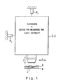
- the optical unit O.U. is shifted in x, y and z directions with respect to the mask and wafer structures.
- the optical unit O.U. is shifted in the z direction by means of a piezo drive P z so that the reference mask patterns are subsequently focused on the mask M and on the wafer W.
- a piezo drive P z By shifting the microscope in the x and y directions (y direction perpendicular to the plane of the sheet of paper, not shown), an alignment of the reference mask patterns with respect to the corresponding patterns in the mask and wafer planes is performed with the piezo drives P x and P y .
- the used piezo drives are piezo-driven tables with a flexure bearing or a universal joint and having an amplitude of approximately 100 ⁇ m with a displacement resolution of 1 nm and a straight motion of 10 nm.
- the optical unit O.U. is tilted about two axes that are perpendicular to each other after the focussing in the z direction with the piezo drive P z .
- Said two axes lie in a plane parallel to the focal plane which is preferably 200 mm spaced apart from the focal plane in the direction of the optical unit O.U.
- the tilting movement is performed by one piezo drive in each case which works in the direction of the tilting and consequently shows a component in the x or y direction.
- the invention can be used for measuring the structural width of photosensitive resist layers. Test results with the system according to the invention were compared and coincided with measurements of a gauged scanning electron microscope in an error range of 50 nm.
Landscapes
- Physics & Mathematics (AREA)
- General Physics & Mathematics (AREA)
- Exposure And Positioning Against Photoresist Photosensitive Materials (AREA)
- Exposure Of Semiconductors, Excluding Electron Or Ion Beam Exposure (AREA)
- Details Of Measuring And Other Instruments (AREA)
Applications Claiming Priority (2)
| Application Number | Priority Date | Filing Date | Title |
|---|---|---|---|
| DE4010880 | 1990-04-04 | ||
| DE4010880A DE4010880C1 (de) | 1990-04-04 | 1990-04-04 |
Publications (3)
| Publication Number | Publication Date |
|---|---|
| EP0450592A2 true EP0450592A2 (de) | 1991-10-09 |
| EP0450592A3 EP0450592A3 (en) | 1992-05-13 |
| EP0450592B1 EP0450592B1 (de) | 1997-08-13 |
Family
ID=6403756
Family Applications (1)
| Application Number | Title | Priority Date | Filing Date |
|---|---|---|---|
| EP91105244A Expired - Lifetime EP0450592B1 (de) | 1990-04-04 | 1991-04-03 | Ausrichtsystem, insbesondere für Röntgen- oder Photolithographie |
Country Status (4)
| Country | Link |
|---|---|
| EP (1) | EP0450592B1 (de) |
| JP (1) | JPH04225515A (de) |
| DE (2) | DE4010880C1 (de) |
| SG (1) | SG54309A1 (de) |
Cited By (2)
| Publication number | Priority date | Publication date | Assignee | Title |
|---|---|---|---|---|
| EP0867775A3 (de) * | 1997-03-27 | 2000-08-02 | Ushiodenki Kabushiki Kaisha | Abstandsbelichtungsvorrichtung mit Vorrichtung zur Einstellung des Abstandes |
| US6950188B2 (en) | 2003-04-23 | 2005-09-27 | International Business Machines Corporation | Wafer alignment system using parallel imaging detection |
Families Citing this family (1)
| Publication number | Priority date | Publication date | Assignee | Title |
|---|---|---|---|---|
| DE10303902B4 (de) * | 2003-01-31 | 2004-12-09 | Süss Microtec Lithography Gmbh | Verfahren und Vorrichtung zum Ausrichten eines Justier-Mikroskops mittels verspiegelter Justiermaske |
Family Cites Families (4)
| Publication number | Priority date | Publication date | Assignee | Title |
|---|---|---|---|---|
| EP0083710B1 (de) * | 1982-01-06 | 1985-08-28 | International Business Machines Corporation | Abgleichsystem für Nah-Abstand-Lithographie |
| US4595295A (en) * | 1982-01-06 | 1986-06-17 | International Business Machines Corporation | Alignment system for lithographic proximity printing |
| US4580900A (en) * | 1982-04-02 | 1986-04-08 | Eaton Corporation | Auto focus alignment and measurement system and method |
| EP0116953A2 (de) * | 1983-02-18 | 1984-08-29 | Hitachi, Ltd. | Ausrichtgerät |
-
1990
- 1990-04-04 DE DE4010880A patent/DE4010880C1/de not_active Expired - Fee Related
-
1991
- 1991-04-03 EP EP91105244A patent/EP0450592B1/de not_active Expired - Lifetime
- 1991-04-03 JP JP3070831A patent/JPH04225515A/ja active Pending
- 1991-04-03 DE DE69127218T patent/DE69127218T2/de not_active Expired - Fee Related
- 1991-04-03 SG SG1996008298A patent/SG54309A1/en unknown
Cited By (2)
| Publication number | Priority date | Publication date | Assignee | Title |
|---|---|---|---|---|
| EP0867775A3 (de) * | 1997-03-27 | 2000-08-02 | Ushiodenki Kabushiki Kaisha | Abstandsbelichtungsvorrichtung mit Vorrichtung zur Einstellung des Abstandes |
| US6950188B2 (en) | 2003-04-23 | 2005-09-27 | International Business Machines Corporation | Wafer alignment system using parallel imaging detection |
Also Published As
| Publication number | Publication date |
|---|---|
| EP0450592A3 (en) | 1992-05-13 |
| SG54309A1 (en) | 1998-11-16 |
| DE69127218T2 (de) | 1997-12-04 |
| DE69127218D1 (de) | 1997-09-18 |
| EP0450592B1 (de) | 1997-08-13 |
| DE4010880C1 (de) | 1991-05-02 |
| JPH04225515A (ja) | 1992-08-14 |
Similar Documents
| Publication | Publication Date | Title |
|---|---|---|
| KR100262992B1 (ko) | 마스크 패턴을 반복적으로 영상화하는 방법 및 그 장치 | |
| JP3074579B2 (ja) | 位置ずれ補正方法 | |
| US6122036A (en) | Projection exposure apparatus and method | |
| US6538740B1 (en) | Adjusting method for position detecting apparatus | |
| JP4029183B2 (ja) | 投影露光装置及び投影露光方法 | |
| JP3572430B2 (ja) | 露光方法及びその装置 | |
| US6225012B1 (en) | Method for positioning substrate | |
| US6583430B1 (en) | Electron beam exposure method and apparatus | |
| JPH10163097A (ja) | 投影露光装置及び投影露光方法 | |
| US6946666B2 (en) | Position detection device, apparatus using the same, exposure apparatus, and device manufacturing method using the same | |
| JP2003151884A (ja) | 合焦方法、位置計測方法および露光方法並びにデバイス製造方法 | |
| US6744512B2 (en) | Position measuring apparatus and exposure apparatus | |
| JP7576194B2 (ja) | マルチビーム画像生成装置およびマルチビーム画像生成方法 | |
| JPH09223650A (ja) | 露光装置 | |
| JP3279979B2 (ja) | ウエハとマスクとの位置検出装置及び変形誤差検出方法 | |
| JP3360744B2 (ja) | アライメント方法、及び走査型露光装置 | |
| KR20000006140A (ko) | 노광방법및노광장치,그리고,이것을이용한디바이스제조방법 | |
| EP0450592B1 (de) | Ausrichtsystem, insbesondere für Röntgen- oder Photolithographie | |
| JPH0581046B2 (de) | ||
| CN1133866C (zh) | 差分干涉仪系统和配有该系统的平版印刷分步扫描装置 | |
| JP3441930B2 (ja) | 走査型露光装置およびデバイス製造方法 | |
| JPH11233398A (ja) | 露光装置及び露光方法 | |
| JP3531227B2 (ja) | 露光方法および露光装置 | |
| JP2006013266A (ja) | 計測方法、露光方法、及び露光装置 | |
| JP2006226719A (ja) | 面形状計測方法、姿勢計測方法、及び露光方法 |
Legal Events
| Date | Code | Title | Description |
|---|---|---|---|
| PUAI | Public reference made under article 153(3) epc to a published international application that has entered the european phase |
Free format text: ORIGINAL CODE: 0009012 |
|
| AK | Designated contracting states |
Kind code of ref document: A2 Designated state(s): CH DE FR GB IT LI NL |
|
| PUAL | Search report despatched |
Free format text: ORIGINAL CODE: 0009013 |
|
| AK | Designated contracting states |
Kind code of ref document: A3 Designated state(s): CH DE FR GB IT LI NL |
|
| 17P | Request for examination filed |
Effective date: 19920911 |
|
| GRAG | Despatch of communication of intention to grant |
Free format text: ORIGINAL CODE: EPIDOS AGRA |
|
| 17Q | First examination report despatched |
Effective date: 19960912 |
|
| GRAH | Despatch of communication of intention to grant a patent |
Free format text: ORIGINAL CODE: EPIDOS IGRA |
|
| GRAH | Despatch of communication of intention to grant a patent |
Free format text: ORIGINAL CODE: EPIDOS IGRA |
|
| GRAA | (expected) grant |
Free format text: ORIGINAL CODE: 0009210 |
|
| AK | Designated contracting states |
Kind code of ref document: B1 Designated state(s): CH DE FR GB IT LI NL |
|
| PG25 | Lapsed in a contracting state [announced via postgrant information from national office to epo] |
Ref country code: IT Free format text: LAPSE BECAUSE OF FAILURE TO SUBMIT A TRANSLATION OF THE DESCRIPTION OR TO PAY THE FEE WITHIN THE PRE;WARNING: LAPSES OF ITALIAN PATENTS WITH EFFECTIVE DATE BEFORE 2007 MAY HAVE OCCURRED AT ANY TIME BEFORE 2007. THE CORRECT EFFECTIVE DATE MAY BE DIFFERENT FROM THE ONE RECORDED.SCRIBED TIME-LIMIT Effective date: 19970813 |
|
| REG | Reference to a national code |
Ref country code: CH Ref legal event code: NV Representative=s name: E. BLUM & CO. PATENTANWAELTE Ref country code: CH Ref legal event code: EP |
|
| REF | Corresponds to: |
Ref document number: 69127218 Country of ref document: DE Date of ref document: 19970918 |
|
| ET | Fr: translation filed | ||
| PLBE | No opposition filed within time limit |
Free format text: ORIGINAL CODE: 0009261 |
|
| STAA | Information on the status of an ep patent application or granted ep patent |
Free format text: STATUS: NO OPPOSITION FILED WITHIN TIME LIMIT |
|
| 26N | No opposition filed | ||
| PGFP | Annual fee paid to national office [announced via postgrant information from national office to epo] |
Ref country code: CH Payment date: 20010420 Year of fee payment: 11 |
|
| REG | Reference to a national code |
Ref country code: GB Ref legal event code: IF02 |
|
| PG25 | Lapsed in a contracting state [announced via postgrant information from national office to epo] |
Ref country code: CH Free format text: LAPSE BECAUSE OF NON-PAYMENT OF DUE FEES Effective date: 20020430 Ref country code: LI Free format text: LAPSE BECAUSE OF NON-PAYMENT OF DUE FEES Effective date: 20020430 |
|
| REG | Reference to a national code |
Ref country code: CH Ref legal event code: PL |
|
| NLS | Nl: assignments of ep-patents |
Owner name: JMAR/SAL NANOLITHOGRAPHY, INC. (A DELAWARE CORPORA Owner name: SUSS MICRO TEC LITOGRAPHY GMBH |
|
| REG | Reference to a national code |
Ref country code: GB Ref legal event code: 732E |
|
| PGFP | Annual fee paid to national office [announced via postgrant information from national office to epo] |
Ref country code: GB Payment date: 20040329 Year of fee payment: 14 |
|
| PGFP | Annual fee paid to national office [announced via postgrant information from national office to epo] |
Ref country code: NL Payment date: 20040419 Year of fee payment: 14 |
|
| PGFP | Annual fee paid to national office [announced via postgrant information from national office to epo] |
Ref country code: FR Payment date: 20040421 Year of fee payment: 14 |
|
| PGFP | Annual fee paid to national office [announced via postgrant information from national office to epo] |
Ref country code: DE Payment date: 20040430 Year of fee payment: 14 |
|
| REG | Reference to a national code |
Ref country code: FR Ref legal event code: CD Ref country code: FR Ref legal event code: TP |
|
| PG25 | Lapsed in a contracting state [announced via postgrant information from national office to epo] |
Ref country code: GB Free format text: LAPSE BECAUSE OF NON-PAYMENT OF DUE FEES Effective date: 20050403 |
|
| PG25 | Lapsed in a contracting state [announced via postgrant information from national office to epo] |
Ref country code: DE Free format text: LAPSE BECAUSE OF NON-PAYMENT OF DUE FEES Effective date: 20051101 Ref country code: NL Free format text: LAPSE BECAUSE OF NON-PAYMENT OF DUE FEES Effective date: 20051101 |
|
| GBPC | Gb: european patent ceased through non-payment of renewal fee |
Effective date: 20050403 |
|
| PG25 | Lapsed in a contracting state [announced via postgrant information from national office to epo] |
Ref country code: FR Free format text: LAPSE BECAUSE OF NON-PAYMENT OF DUE FEES Effective date: 20051230 |
|
| NLV4 | Nl: lapsed or anulled due to non-payment of the annual fee |
Effective date: 20051101 |
|
| REG | Reference to a national code |
Ref country code: FR Ref legal event code: ST Effective date: 20051230 |