EP0450831A2 - Circuit pour alimenter une lampe à décharge - Google Patents
Circuit pour alimenter une lampe à décharge Download PDFInfo
- Publication number
- EP0450831A2 EP0450831A2 EP91302609A EP91302609A EP0450831A2 EP 0450831 A2 EP0450831 A2 EP 0450831A2 EP 91302609 A EP91302609 A EP 91302609A EP 91302609 A EP91302609 A EP 91302609A EP 0450831 A2 EP0450831 A2 EP 0450831A2
- Authority
- EP
- European Patent Office
- Prior art keywords
- lamp
- voltage
- inductor
- power circuit
- gas discharge
- Prior art date
- Legal status (The legal status is an assumption and is not a legal conclusion. Google has not performed a legal analysis and makes no representation as to the accuracy of the status listed.)
- Granted
Links
Images




Classifications
-
- D—TEXTILES; PAPER
- D01—NATURAL OR MAN-MADE THREADS OR FIBRES; SPINNING
- D01G—PRELIMINARY TREATMENT OF FIBRES, e.g. FOR SPINNING
- D01G31/00—Warning or safety devices, e.g. automatic fault detectors, stop motions
-
- H—ELECTRICITY
- H05—ELECTRIC TECHNIQUES NOT OTHERWISE PROVIDED FOR
- H05B—ELECTRIC HEATING; ELECTRIC LIGHT SOURCES NOT OTHERWISE PROVIDED FOR; CIRCUIT ARRANGEMENTS FOR ELECTRIC LIGHT SOURCES, IN GENERAL
- H05B41/00—Circuit arrangements or apparatus for igniting or operating discharge lamps
- H05B41/14—Circuit arrangements
- H05B41/26—Circuit arrangements in which the lamp is fed by power derived from DC by means of a converter, e.g. by high-voltage DC
- H05B41/28—Circuit arrangements in which the lamp is fed by power derived from DC by means of a converter, e.g. by high-voltage DC using static converters
- H05B41/288—Circuit arrangements in which the lamp is fed by power derived from DC by means of a converter, e.g. by high-voltage DC using static converters with semiconductor devices and specially adapted for lamps without preheating electrodes, e.g. for high-intensity discharge lamps, high-pressure mercury or sodium lamps or low-pressure sodium lamps
- H05B41/2881—Load circuits; Control thereof
- H05B41/2882—Load circuits; Control thereof the control resulting from an action on the static converter
-
- H—ELECTRICITY
- H05—ELECTRIC TECHNIQUES NOT OTHERWISE PROVIDED FOR
- H05B—ELECTRIC HEATING; ELECTRIC LIGHT SOURCES NOT OTHERWISE PROVIDED FOR; CIRCUIT ARRANGEMENTS FOR ELECTRIC LIGHT SOURCES, IN GENERAL
- H05B41/00—Circuit arrangements or apparatus for igniting or operating discharge lamps
- H05B41/14—Circuit arrangements
- H05B41/36—Controlling
- H05B41/38—Controlling the intensity of light
- H05B41/382—Controlling the intensity of light during the transitional start-up phase
- H05B41/388—Controlling the intensity of light during the transitional start-up phase for a transition from glow to arc
-
- Y—GENERAL TAGGING OF NEW TECHNOLOGICAL DEVELOPMENTS; GENERAL TAGGING OF CROSS-SECTIONAL TECHNOLOGIES SPANNING OVER SEVERAL SECTIONS OF THE IPC; TECHNICAL SUBJECTS COVERED BY FORMER USPC CROSS-REFERENCE ART COLLECTIONS [XRACs] AND DIGESTS
- Y02—TECHNOLOGIES OR APPLICATIONS FOR MITIGATION OR ADAPTATION AGAINST CLIMATE CHANGE
- Y02B—CLIMATE CHANGE MITIGATION TECHNOLOGIES RELATED TO BUILDINGS, e.g. HOUSING, HOUSE APPLIANCES OR RELATED END-USER APPLICATIONS
- Y02B20/00—Energy efficient lighting technologies, e.g. halogen lamps or gas discharge lamps
-
- Y—GENERAL TAGGING OF NEW TECHNOLOGICAL DEVELOPMENTS; GENERAL TAGGING OF CROSS-SECTIONAL TECHNOLOGIES SPANNING OVER SEVERAL SECTIONS OF THE IPC; TECHNICAL SUBJECTS COVERED BY FORMER USPC CROSS-REFERENCE ART COLLECTIONS [XRACs] AND DIGESTS
- Y02—TECHNOLOGIES OR APPLICATIONS FOR MITIGATION OR ADAPTATION AGAINST CLIMATE CHANGE
- Y02P—CLIMATE CHANGE MITIGATION TECHNOLOGIES IN THE PRODUCTION OR PROCESSING OF GOODS
- Y02P70/00—Climate change mitigation technologies in the production process for final industrial or consumer products
- Y02P70/50—Manufacturing or production processes characterised by the final manufactured product
- Y02P70/62—Manufacturing or production processes characterised by the final manufactured product related technologies for production or treatment of textile or flexible materials or products thereof, including footwear
-
- Y—GENERAL TAGGING OF NEW TECHNOLOGICAL DEVELOPMENTS; GENERAL TAGGING OF CROSS-SECTIONAL TECHNOLOGIES SPANNING OVER SEVERAL SECTIONS OF THE IPC; TECHNICAL SUBJECTS COVERED BY FORMER USPC CROSS-REFERENCE ART COLLECTIONS [XRACs] AND DIGESTS
- Y10—TECHNICAL SUBJECTS COVERED BY FORMER USPC
- Y10S—TECHNICAL SUBJECTS COVERED BY FORMER USPC CROSS-REFERENCE ART COLLECTIONS [XRACs] AND DIGESTS
- Y10S315/00—Electric lamp and discharge devices: systems
- Y10S315/02—High frequency starting operation for fluorescent lamp
-
- Y—GENERAL TAGGING OF NEW TECHNOLOGICAL DEVELOPMENTS; GENERAL TAGGING OF CROSS-SECTIONAL TECHNOLOGIES SPANNING OVER SEVERAL SECTIONS OF THE IPC; TECHNICAL SUBJECTS COVERED BY FORMER USPC CROSS-REFERENCE ART COLLECTIONS [XRACs] AND DIGESTS
- Y10—TECHNICAL SUBJECTS COVERED BY FORMER USPC
- Y10S—TECHNICAL SUBJECTS COVERED BY FORMER USPC CROSS-REFERENCE ART COLLECTIONS [XRACs] AND DIGESTS
- Y10S315/00—Electric lamp and discharge devices: systems
- Y10S315/07—Starting and control circuits for gas discharge lamp using transistors
Definitions
- the present invention relates to a power circuit that supplies DC excitation to a gas discharge lamp.
- Embodiments of the present invention relate to a ballast circuit that automatically and sequentially provides desired transfer functions for the DC operation of the metal halide lamp.
- the ballast circuit having its desired transfer functions provides the necessary voltage and current conditions to the gas discharge lamp, such as a metal halide lamp, so that it properly performs during its various modes of operation which are; (1) an initial high voltage breakdown or start mode; (2) a glow-to-arc transition or glow mode; and (3) a steady state, arc or run mode.
- Each of these modes have different voltage and current requirements allowing the gas discharge lamp to perform in a proper manner. It is desired that these various current and voltage requirements be provided in an automatic and sequential manner so that the lamp transitions from its start, to its glow, and then to its run mode. Similarly, it is desired that these voltage and current conditions be automatically provided if the lamp reverts from its run mode to its glow or start mode.
- the current developed by the ballast circuit which flows through the gas discharge lamp may typically experience surges as these lamps enter or revert from its modes of operation, for example, as the lamp ionizes and enters into the glow mode, the current flowing at this entrance is of a relatively large value and is of a relatively high rate of change which may be such so as to detrimentally affect the associated circuit components of ballast circuit and especially the lamp itself. It is desired that a ballast circuit be provided with means to limit the maximum amount of current supplied to the lamp during its modes of operation and also to limit the related maximum rate of change of the current.
- Ballast circuits commonly comprise impedance devices that are utilized for supplying the necessary conditions for operating a gas discharge lamp. These impedance devices in ballast circuit operated from a typical AC power source create an undesirable condition with regard to lowering the related power factor which, in turn, causes a leading or lagging current relative to the AC power source. The resulting low power factor becomes a concern to the lighting installation designers who must size the conductors and to the electric power companies who must provide the additional reactive power. It is desired that a ballast circuit be provided with means that are easily adapted to present a high power factor to a power source of not less than 0.90. It is especially desired to present this high power factor during the steady-state or run mode of the lamp.
- Illustrative embodiments of the present invention as disclosed herein seek to provide: a ballast circuit having means for easily adapting and presenting a high power factor to the AC power source supplying the gas discharge lamp; a ballast circuit that presents the desired current and voltage conditions to the gas discharge lamp, in an automatic manner, so that the lamp is allowed to transition to or revert from its start, glow or run modes of operation while still yielding proper lamp performance; and/or a ballast circuit having means that limits the amount of current and the rate-of-change of the current supplied to the lamp during its start, glow and run modes of operation.
- a ballast circuit for operating a gas discharge lamp from an AC source by supplying, automatically and sequentially, DC excitation during the start, glow and run modes of operation.
- the ballast circuit comprises an input filter stage, a AC to DC converter, and an oscillator having an electronic switching device with predetermined breakdown characteristics.
- the input filter stage comprises capacitors and an inductor with one of the capacitors having an impedance value selected to present a relatively high power factor to the AC power source especially during the run mode of operation of the lamp.
- the AC to DC converter has an output stage whose DC voltage is dependent upon the impedance value of the gas discharge lamp during its start, glow and run modes of operation.
- the oscillator is connected to the output stage of the AC to DC converter and has an output stage comprised of components including a first inductor as a means of coupling the oscillator output to the lamp with the other components controlling the frequency of operation.
- the breakdown characteristic of the switching means of the oscillator is selected such that the switching means is (1) rendered conductive when the DC voltage at the output stage corresponds to the impedance value of the gas discharge lamp during its starting mode, and (2) maintained non-conductive condition when the DC voltage at the output stage of the AC to DC converter corresponds to the impedance value of the gas discharge lamp during its run mode of operation.
- Fig. 1 illustrates a schematic of a ballast circuit 10 for operating a gas discharge lamp 12.
- the gas discharge lamp 12 may be of the high efficient metal halide type described in U.S. Patent 4,161,672 of D. M. Cap and Lake issued July 17, 1979 or any DC operating lamp which exhibits a gaseous discharge.
- the ballast circuit 10 comprises an input filter stage 14, a AC to DC converter 16, and a starting circuit 18.
- the ballast circuit 10 may receive its excitation from a typical AC power source 20 having a voltage of about 120 volts AC and a frequency of 60Hz.
- Other power sources 20 may find application to the present invention such as those found in Japan and European countries.
- the ballast circuit 10 comprises a plurality of the conventional elements of the type indicated or having typical components value both as given in Table 1.
- the ballast circuit 10 operates the discharge lamp 12 by the application of various levels of DC excitation during its start, glow and run modes.
- the type and values of the circuit components given in Table 1 of the ballast circuit 10 are selected so as to automatically and sequentially provide desired transfer functions of the circuit 10 that are determined and interrelated to the impedance values of the lamp occurring during its start, glow and run modes.
- the ballast circuit 10 automatically provides these functions for the lamp as it transitions into or reverts from its start, glow and run modes of operation.
- the ballast circuit 10 provides DC excitation to the lamp 12 which includes the necessary voltages and current conditions so as to transition the gas discharge lamp 12 from its (1) initial state requiring a high applied voltage of about a 1KV to cause an initial break down of the gas discharge lamp, which causes the lamp to (2) enter its positive resistance region commonly referred to as its glow mode that requires a compliance or glow voltage of about 300 volts, and then transitions the lamp to (3) its final arc or run mode.
- the high voltage 1KV is applied and then reapplied until the lamp obtains its start condition.
- the starting signal developed by the starting circuit improves or aids in the starting of the discharge lamp relative to prior methods.
- the DC voltage applied to the lamp changes from the compliance or glow voltage of about 300 volts to about 30 volts and then slowly rises to about 90 volts during the run mode.
- the input filter stage 14 of ballast 10 of Fig. 1 is arranged across the power source 20 in a ⁇ type and comprises capacitors C1 and C2 and an inductor L1.
- one of the capacitors C1 has an impedance value selected so as to cause the ballast circuit 10 to present a relatively high power factor to the AC source 20 during the run mode of the lamp 12.
- the components L1 and C2 form an LC circuit whose undampened resonant frequency is about 80Hz.
- This LC circuit amplifies the 120 volts 60 cycle signal from the power source 20 to approximately 300 volts which is applied to the AC to DC converter 16.
- the AC to DC converter 16 is comprised of diodes D1 through D4 arranged as a full wave rectifier which provides DC output voltage that is preferably filtered by capacitor C3.
- the DC voltage at the output stage of the AC to DC converter 16 is dependent or determined by the impedance value R ⁇ of the gas discharge lamp which sequences in a downward manner during the start, glow and run modes and may be further discussed with reference to Fig. 2.
- Fig. 2 shows the components of Fig. 1 that are effective as to a first order approximation, that is with 10%, of the circuit during the run mode.
- Fig. 2 represents an intermediate illustration in the establishment of the equivalent circuit related to the run mode.
- T1 is shown as comprising two windings T 1A and T 1B which act as two mutually coupled inductors.
- the transformer T1 merely operates as an inductor to filter the AC component of the rectified current.
- the equivalent circuit of the run circuit may be as shown in Fig. 3.
- Fig. 3 is similar to Fig. 2 in that it illustrates the input stage 14 but is different thereto in that it shows L1 as comprised of a series resistance R1 and an inductance L.
- Fig. 3 represents the equivalent circuit related to the run mode.
- Fig. 3 illustrates the equivalent circuit in a two-port network manner.
- V2 is an AC voltage corresponding to the reflected lamp voltage capable of being measured across C2.
- the current flowing through L1 and R1 is termed I.
- R2 The resistance across the V2 is termed R2 which is substantially greater than the series resistance R1 and has a value represented by expression3 shown in Appendix A.
- the condition of the currents and voltages shown in the equivalent circuit of Fig. 3 is expressed by the transfer function G1 shown in expression (4) of Appendix A.
- the transfer function G1 of expression (4) is represented in terms of (1) damping factor ⁇ , (4) the frequency ( ⁇ ) of V1 in radians/second, (3) the natural frequency ( ⁇ n ) of the filter 14 in radians/second and in terms of the (4) resistor, capacitor and inductor components shown Fig. 3.
- the transfer function of expression (4) illustrates that the circuit composed of L1 and C2 responds to any and all load demands, as mandated by the lamp characteristics, to establish the proper voltage and current for the lamp during the three modes of operation, start, glow and run.
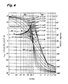
- the transfer function of expression (4) is plotted in Fig. 4 with the damping factor being the implicit variable.
- Fig. 4 has an X coordinate represented of the quantity ⁇ / ⁇ n from 0.1 to 8.0 shown by the log10 grids.
- the first quantity L m is measured in decibels (db).
- the second Y coordinate represents the phase angle between the source 20 and the reflected lamp voltage as discussed with regard to R2 of Fig. 3 and is given in degrees.
- the quantity L m is shown as having a range of -30 db to 15db, whereas, the phase angle is shown as having a 0 degree (in-phase) to -180 degree range.
- Fig. 4 shows a plot of a family of characteristic curves having damping factors with values shown as being grouped under under 22 A of 0.10, 0.15, 0.20, 0.25, 0.30, 0.50, 0.71, and 1.00. These values 22 A are interrelated to (1) an upper plot of curve portions 22 B , (2) a central plot of curve portions 22 C and (3) a lower plot of curve portions 22 D .
- the upper plots 22 B and the lower plots 22 D are continuous and focus or merge at the intersection of L m of about -7.5 db, a phase angle of 90°, and a quantity ⁇ / ⁇ n of 1.0.
- the 12 db/octave break-point related to the lower merger point of the quantities of 22 A is shown in Fig. 4 by reference number 24.
- the load trajectory 26 associated with the various operational modes of circuit 10 is superimposed on the family of the characteristic curves primarily related to plot 22 C as shown in Fig. 4.
- the desired operating point for the glow mode is shown on the load trajectory by reference number 28, whereas, the desired operating point for the run mode is shown by reference number 30.
- Operating point 30 lies directly on the plot 22 C related to damping factor 0.71 curve, whereas, operating point 28 lies directly on the plot 22 related to damping factor 0.10.
- the steady-state operating point 30 moves (travel) on the vertical load trajectory line 26. For example, the operating point moves from a damping factor curve 0.71 upward toward a damping factor curve of 0.5.
- the power source 20 represented in Fig. 3 as V1 changes, the operating point 30 similarly move either above or below the operating point 30 of that shown in Fig. 4. It is desired that the operating point 30 of the run mode not fall below the 0.5 damping factor value.
- the operation of the ballast circuit 10 during the run mode of the gas discharge lamp 12 may be further described with reference to expressions (5) and (6) of Appendix A both related to transfer function G2 representative of the input of the circuit of Fig. 3 as it may appear to the applied voltage V1.
- the transfer function G2 illustrates that when the run circuit is loaded by the lamp, the circuit reacts in such a way as to establish a current whose phase angle with respect to the power line voltage is easily corrected by a single reactive component C1 in a manner to be described.
- the terms in expressions (5) and (6) are the same as those described with regard to expressions (3) and (4) except for the addition of Z o which is the characteristic impedance of the filter 14 expressed in terms of L1 and C2. It should be noted that C1 is lacking in any of the terms of expressions (3) and (4).
- the void of C1 is intended so as to describe the background for the effect of C1 in the easily obtainable desired power factor.
- Fig. 5 has an ordinate showing the phase angle ⁇ ( ⁇ ) between I and V1 having a peak of about a positive +90° and a valley of about a -90°.
- Fig. 5 also has an abscissa representative of the damping factor ⁇ and showing the previously discussed, with regard to Fig. 4, damping factor quantity 0.71 related to the run mode of ballast 10.
- Fig. 5 shows the intersection of the damping factor of 0.71 as corresponding to an angle of -45°. This phase angle of -45 is corrected by the present embodiment by providing a nearly unity power factor caused by the selection of the value of capacitor C1.
- the value of C1 may be selected in the range of 1.5 to 3.0 microfarads.
- One of the advantages of the input filter 14 having the capacitor C1 is that a desired power factor is easilyobtained by the selection of the value of a single capacitive component C1.
- This easy selectable capacitive method to provide the power factor correction is due in part to the nearly sinusoidal nature of I occurring during the run mode of operation. This method provides a power factor of not less than 0.90.
- the values of C1 from 1.5 to 3.0 microfarad are related to a typical 60 Hz power. These desired values change as the frequency of the power sources changes such as to those found in Europe and Japan. Further, if desired, the 3.0 microfarad value may be exceeded so that the phase angle ⁇ ( ⁇ ) may become a positive (+) or leading quantity. Thus there is an ability to select a single component to provide for the desired phase angle ⁇ ( ⁇ ).
- the designer first establishes the desired amplification needed for the compliance voltage obtained by the selection of the values of L1 and C2. Then the designer may determine the desired transfer functions for the desired run operation of the lamp. Finally the designer may then select a particular value for C1 to provide for the desired power factor.
- the lamp 12 Prior to the attainment of the run mode of operation, the lamp 12 passes through the glow mode.
- the lamp 12 In the glow mode, the lamp 12 requires about 300 volts DC for its compliance or glow voltage and about 10 milliamps of current in order for the lamp to establish an arc condition to allow it to pass into the run mode.
- the ballast 10 accepts the power line voltage which can vary from 108 to 132 volts and amplifies such by the operation of the resonant network L1 and C2.
- Network 16 of Fig. 1 then rectifies the output of L1-C2 to about 300 volts DC.
- This damping factor of 0.00833 is added to by the residue values components (e.g., C4 and R5) of the start circuit, to be discussed, and results in an equivalent damping factor of approximately 0.1. As seen in Fig. 4, this damping factor of 0.1 provides sufficient amplification of 7db (about 2.4) so as to transition the lamp into the run mode.
- the needed circuitry for the individual modes of lamp operation is segmented and automatically and sequentially provides the desired circuit transfer functions.
- the glow circuit which is primarily comprised of the elements shown in Fig. 2 (including C3 (not shown) of AC to DC converter 16) is automatically activated if the arc condition occurring during the run mode of the lamp extinguishes for any reason.
- the start circuit is automatically activated whenever the lamp current extinguishes in either the run or glow modes because the sidac S1 of Fig. 1 and 6 is rendered conductive whenever the voltage output of the AC to DC converter is greater than 240 volts which corresponds to the breakdown characteristic of S1.
- the start circuit that employs the sidac S1 may be further described with reference to Fig. 6.
- the starting circuit 18 of Fig. 6 develops a relatively high DC voltage level (about 1200V DC) upon which occurs pulses (about 300V DC) having a repetition rate of about 2.5m sec.
- this signal is developed by an oscillator circuit whose voltage output is amplified by T1, rectified by D6 and D8 and filtered by C5 as a means to produce a nearly DC voltage of sufficient amplitude to cause the lamp to conduct.
- the developed signal provides for better starting of the discharge lamp relative to prior art methods.
- the sidac S1 of the start circuit 18 is selected to have breakdown voltage characteristic such that it is; (1) rendered conductive when the DC voltage, for example 300 volts, at the output stage of the converter 16 corresponds the impedance value, such as 500K ohms, of the gas discharge lamp occurring during its starting mode; and (2) is maintained in its non-conductive state when the DC voltages of less than 240 volts and less than about 90 volts correspond to the impedance value of the gas discharge lamp such as 250 ⁇ and 30K occurring during the run and glow modes respectively.
- the output of the AC to DC converter 16 exceeds about 240V DC (typically at about 300V DC), it excites a 400Hz relaxation oscillator comprised of R4, C4, S1 and T 1A in which the values of R4 and C4 primarily determine the frequency of oscillation.
- the 300V DC level causes sidac S1 to be rendered conductive, which, in turn causes capacitor C4 serving as a first energy storage means and having a stored value of about 240V to discharge into T1 having a mutually coupled winding to establish a high voltage.
- T1 having the windings T 1A and T 1B develops a voltage of,about 960V which is additive with 240V of C4 and the 300V of the converter 16 so as to generate a voltage of about 1500V across T1 which is shown as a pulsed waveform 32 across T 1B .
- This 1500V signal is rectified by diodes D6 and D8 along with diode D7 which directs the 1500V DC signal to charge a second energy storage device capacitor C5.
- This signal also appears at the input to L2, via resistor R6 which prevents rapid discharging of C5, and is shown as signal 34.
- Signal 34 is shown as a pulse waveform having a peak amplitude of about 1500V DC which decays to a value of about 1200V DC.
- the time constant decay of signal 34 is about 10m sec. and is determined by the value selected for C5 (0.22 microfarads) and the impedance value (about 500k) of lamp 12.
- the signal 34 has a repetition rate of about 2.5m seconds. The characteristics of signal 34, in particular the high DC level having the pulses extending therefrom, provides for easier starting of the discharge lamp relative to prior methods.
- the starting circuit 18 preferably further includes an inductor L2 connected to the arrangement of diodes D8 and D6.
- the inductor has a value selected, previously given, to limit the amplitude and the rate of change of the current applied to the lamp during the entrance to the glow mode from the start mode.
- the two diodes D8 and D6 shown in Fig. 6 may be replaced with a single high voltage type diode.
- the resistor R6 in addition to providing a path for the development of signal 34 also reduces the susceptibility of the lamp to "back arcing" by increasing the impedance path from the lamp 12 to the capacitor C5.
- back arcing it is meant that an arc strikes off the back of one of the electrodes of the lamp typically caused by high di/dt conditions experienced by lamp 12.
- the diode D7 facilitates the charging of C5, which reduces the high voltage ripple to which lamp 12 is subjected.
- the charging time of C5 is related to C5 and the series resistance of T 1B .
- a diode D5 be included in the starting circuit and arranged so as to be reversed biased when the switching means S1 is in its non-conductive state.
- D5 performs a clamping function in that the output of T 1B (side attached to D5, D6 and D7) will go negative (voltage) each time the current through sidac S1 is abruptly stopped.
- the diode D5 clamps this negative voltage and prevents D6 and D8 from being damaged due to excessive reverse voltage.
- the inductor T1 of the starting circuit 18 is preferably a tapped inductor and is used instead of a transformer so as to provide a step-up function for the development of signal 34.
- the usage of the tapped inductor improves the manufacturability of the power circuit and decreases the cost while at the same time improving the efficiency of the high voltage circuit.
- ballast circuit 10 Further improvement for the ballast circuit 10 is shown in Fig. 1 with reference to the resistors R5 and R3.
- the resistor R5 is of a low value and in actuality is a fuse serving as a protection function.
- the resistor R3 provides a bleeder function to provide a path for the discharging of C1 and C2.
- the ballast circuit having the desired transfer functions that automatically sequence as the lamp transitions from its (1) start to its (2) glow, and then to its (3) run modes of operation.
- the desired transfer impedance is automatically obtained during any of the operating modes of the metal halide lamp.
Landscapes
- Engineering & Computer Science (AREA)
- Textile Engineering (AREA)
- Circuit Arrangements For Discharge Lamps (AREA)
Applications Claiming Priority (2)
| Application Number | Priority Date | Filing Date | Title |
|---|---|---|---|
| US505100 | 1990-04-03 | ||
| US07/505,100 US5059867A (en) | 1990-04-03 | 1990-04-03 | Ballast circuit with improved transfer functions |
Publications (3)
| Publication Number | Publication Date |
|---|---|
| EP0450831A2 true EP0450831A2 (fr) | 1991-10-09 |
| EP0450831A3 EP0450831A3 (en) | 1991-12-18 |
| EP0450831B1 EP0450831B1 (fr) | 1994-11-23 |
Family
ID=24009021
Family Applications (1)
| Application Number | Title | Priority Date | Filing Date |
|---|---|---|---|
| EP91302609A Expired - Lifetime EP0450831B1 (fr) | 1990-04-03 | 1991-03-26 | Circuit pour alimenter une lampe à décharge |
Country Status (5)
| Country | Link |
|---|---|
| US (1) | US5059867A (fr) |
| EP (1) | EP0450831B1 (fr) |
| JP (1) | JP2593593B2 (fr) |
| CA (1) | CA2038221C (fr) |
| DE (1) | DE69105227T2 (fr) |
Cited By (3)
| Publication number | Priority date | Publication date | Assignee | Title |
|---|---|---|---|---|
| WO1996031095A1 (fr) * | 1995-03-29 | 1996-10-03 | Stebbins Russell T | Procede et dispositif pour eclairage par ionisation pulsee a courant continu |
| WO1997021329A1 (fr) * | 1995-12-01 | 1997-06-12 | Robert Bosch Gmbh | Circuit d'amorçage pour lampe a decharge a haute pression |
| WO1999012403A1 (fr) * | 1997-09-01 | 1999-03-11 | Koninklijke Philips Electronics N.V. | Montage |
Families Citing this family (7)
| Publication number | Priority date | Publication date | Assignee | Title |
|---|---|---|---|---|
| DE9015674U1 (de) * | 1990-11-15 | 1992-03-12 | Patent-Treuhand-Gesellschaft für elektrische Glühlampen mbH, 8000 München | Getaktetes Schaltnetzteil für den Betrieb einer Entladungslampe |
| US5313142A (en) * | 1992-03-05 | 1994-05-17 | North American Philips Corporation | Compact fluorescent lamp with improved power factor |
| US5387848A (en) * | 1992-03-05 | 1995-02-07 | Philips Electronics North America Corporation | Fluorescent lamp ballast with regulated feedback signal for improved power factor |
| US5317237A (en) * | 1992-03-27 | 1994-05-31 | General Electric Company | Low voltage ballast circuit for a high brightness discharge light source |
| TW299558B (fr) * | 1992-04-03 | 1997-03-01 | Hubbell Inc | |
| DE4423275A1 (de) * | 1994-07-05 | 1996-01-11 | Bosch Gmbh Robert | Zündvorrichtung für Gasentladungslampen, insbesondere für Kraftfahrzeugleuchten |
| CN106192085A (zh) * | 2016-08-28 | 2016-12-07 | 江苏泰达纺织有限公司 | 一种a076给棉罗拉控制电路 |
Family Cites Families (20)
| Publication number | Priority date | Publication date | Assignee | Title |
|---|---|---|---|---|
| US3913002A (en) * | 1974-01-02 | 1975-10-14 | Gen Electric | Power circuits for obtaining a high power factor electronically |
| US3890537A (en) * | 1974-01-02 | 1975-06-17 | Gen Electric | Solid state chopper ballast for gaseous discharge lamps |
| US4161672A (en) * | 1977-07-05 | 1979-07-17 | General Electric Company | High pressure metal vapor discharge lamps of improved efficacy |
| DE2938529C2 (de) * | 1979-09-24 | 1981-10-15 | Siemens AG, 1000 Berlin und 8000 München | Zünd- und Betriebsgerät für eine Hochdrucklampe |
| JPS6016080B2 (ja) * | 1980-08-20 | 1985-04-23 | ウシオ電機株式会社 | 直流放電灯点灯装置 |
| AT369609B (de) * | 1980-09-11 | 1983-01-25 | Elger Elektro Neon | Schaltungsanordnung fuer den betrieb von gasentladungslampen |
| US4415837A (en) * | 1981-11-05 | 1983-11-15 | International Telephone And Telegraph Corporation | Starting circuit for gaseous discharge lamps |
| US4494045A (en) * | 1983-04-26 | 1985-01-15 | General Electric Company | Ballast circuit for a 220-volt improved lighting unit |
| US4626745A (en) * | 1983-04-26 | 1986-12-02 | General Electric Company | Ballast circuit for lamps with low voltage gas discharge tubes |
| US4572988A (en) * | 1983-08-22 | 1986-02-25 | Industrial Design Associates, (Ida) | High frequency ballast circuit |
| US4567404A (en) * | 1983-12-19 | 1986-01-28 | General Electric Company | Ballast circuit having electromagnetic interference (EMI) reducing means for an improved lighting unit |
| JPH0245461Y2 (fr) * | 1984-09-26 | 1990-12-03 | ||
| US4678968A (en) * | 1985-02-15 | 1987-07-07 | Gte Products Corporation | High intensity discharge lamp starting and operating apparatus |
| JPS62100996A (ja) * | 1985-10-29 | 1987-05-11 | 株式会社 デンコ−社 | 螢光放電灯点灯装置 |
| JPS63109217A (ja) * | 1986-10-28 | 1988-05-13 | Mazda Motor Corp | エンジンの排気サイレンサ構造 |
| US4749913A (en) * | 1987-04-17 | 1988-06-07 | General Electric Company | Operating circuit for a direct current discharge lamp |
| US4916364A (en) * | 1988-07-27 | 1990-04-10 | General Electric Company | Parallel arranged starting circuit for gaseous discharge lamps |
| US4945278A (en) * | 1988-09-20 | 1990-07-31 | Loong-Tun Chang | Fluorescent tube power supply |
| US4952847A (en) * | 1989-06-05 | 1990-08-28 | Lin Tieng Fu | Stable ignition means for fluorescent lamp or the like |
| JP5323632B2 (ja) | 2009-09-29 | 2013-10-23 | トッパン・フォームズ株式会社 | Icカードのデータ表示方法及びicカード |
-
1990
- 1990-04-03 US US07/505,100 patent/US5059867A/en not_active Expired - Fee Related
-
1991
- 1991-03-14 CA CA002038221A patent/CA2038221C/fr not_active Expired - Fee Related
- 1991-03-26 DE DE69105227T patent/DE69105227T2/de not_active Expired - Fee Related
- 1991-03-26 EP EP91302609A patent/EP0450831B1/fr not_active Expired - Lifetime
- 1991-04-02 JP JP3094971A patent/JP2593593B2/ja not_active Expired - Lifetime
Cited By (4)
| Publication number | Priority date | Publication date | Assignee | Title |
|---|---|---|---|---|
| WO1996031095A1 (fr) * | 1995-03-29 | 1996-10-03 | Stebbins Russell T | Procede et dispositif pour eclairage par ionisation pulsee a courant continu |
| US5698952A (en) * | 1995-03-29 | 1997-12-16 | Stebbins; Russell T. | Method and apparatus for direct current pulsed ionization lighting |
| WO1997021329A1 (fr) * | 1995-12-01 | 1997-06-12 | Robert Bosch Gmbh | Circuit d'amorçage pour lampe a decharge a haute pression |
| WO1999012403A1 (fr) * | 1997-09-01 | 1999-03-11 | Koninklijke Philips Electronics N.V. | Montage |
Also Published As
| Publication number | Publication date |
|---|---|
| DE69105227D1 (de) | 1995-01-05 |
| DE69105227T2 (de) | 1995-07-13 |
| JP2593593B2 (ja) | 1997-03-26 |
| US5059867A (en) | 1991-10-22 |
| JPH04249892A (ja) | 1992-09-04 |
| EP0450831A3 (en) | 1991-12-18 |
| CA2038221C (fr) | 2000-11-28 |
| CA2038221A1 (fr) | 1991-10-04 |
| EP0450831B1 (fr) | 1994-11-23 |
Similar Documents
| Publication | Publication Date | Title |
|---|---|---|
| KR100289019B1 (ko) | 램프 밸러스트 회로 | |
| US4952848A (en) | Signal generating circuit for ballast control of discharge lamps | |
| US5289083A (en) | Resonant inverter circuitry for effecting fundamental or harmonic resonance mode starting of a gas discharge lamp | |
| US6603274B2 (en) | Dimming ballast for compact fluorescent lamps | |
| US4958107A (en) | Switching arrangement for HID lamps | |
| US5528484A (en) | Power supply | |
| CA2083011A1 (fr) | Ballast pour lampe fluorescente compacte, a faible harmonique | |
| EP0763312A1 (fr) | Configuration de circuit | |
| US4107579A (en) | Starting and operating ballast for high pressure sodium lamp | |
| EP0059053A2 (fr) | Alimentation de courant à impulsions | |
| US5012161A (en) | Power factor correction circuit | |
| EP0098285A1 (fr) | Dispositif electronique commande a haute frequence pour l'allumage de lampes a decharge gazeuse. | |
| EP0450831B1 (fr) | Circuit pour alimenter une lampe à décharge | |
| EP0622888B1 (fr) | Alimentation en courant continu avec un facteur de puissance amélioré | |
| EP0808086A1 (fr) | Ballast en demi-pont pour lampes à décharge, attaqué par un circuit intégré à haute tension | |
| US6362576B1 (en) | Circuit arrangement for igniting a lamp | |
| AU642862B2 (en) | Circuit and method for driving and controlling gas discharge lamps | |
| AU609388B2 (en) | High frequency ballast for gaseous discharge lamps | |
| EP0212817B1 (fr) | Onduleurs | |
| JPS61260598A (ja) | ガス放電灯点灯回路配置 | |
| JPS60207295A (ja) | 高圧ガス放電ランプ用の交流動作回路 | |
| KR20020087146A (ko) | 고압 램프용 전자식 안정기 | |
| JPH034492A (ja) | 放電ランプ用安定回路 | |
| JP3323521B2 (ja) | 放電灯点灯装置 | |
| CN1188588A (zh) | 电路 |
Legal Events
| Date | Code | Title | Description |
|---|---|---|---|
| PUAI | Public reference made under article 153(3) epc to a published international application that has entered the european phase |
Free format text: ORIGINAL CODE: 0009012 |
|
| AK | Designated contracting states |
Kind code of ref document: A2 Designated state(s): DE FR GB NL |
|
| PUAL | Search report despatched |
Free format text: ORIGINAL CODE: 0009013 |
|
| AK | Designated contracting states |
Kind code of ref document: A3 Designated state(s): DE FR GB NL |
|
| 17P | Request for examination filed |
Effective date: 19911220 |
|
| 17Q | First examination report despatched |
Effective date: 19930714 |
|
| GRAA | (expected) grant |
Free format text: ORIGINAL CODE: 0009210 |
|
| AK | Designated contracting states |
Kind code of ref document: B1 Designated state(s): DE FR GB NL |
|
| REF | Corresponds to: |
Ref document number: 69105227 Country of ref document: DE Date of ref document: 19950105 |
|
| ET | Fr: translation filed | ||
| PLBE | No opposition filed within time limit |
Free format text: ORIGINAL CODE: 0009261 |
|
| STAA | Information on the status of an ep patent application or granted ep patent |
Free format text: STATUS: NO OPPOSITION FILED WITHIN TIME LIMIT |
|
| 26N | No opposition filed | ||
| REG | Reference to a national code |
Ref country code: GB Ref legal event code: IF02 |
|
| PGFP | Annual fee paid to national office [announced via postgrant information from national office to epo] |
Ref country code: FR Payment date: 20020304 Year of fee payment: 12 |
|
| PGFP | Annual fee paid to national office [announced via postgrant information from national office to epo] |
Ref country code: NL Payment date: 20020305 Year of fee payment: 12 |
|
| PGFP | Annual fee paid to national office [announced via postgrant information from national office to epo] |
Ref country code: GB Payment date: 20020320 Year of fee payment: 12 Ref country code: DE Payment date: 20020320 Year of fee payment: 12 |
|
| PG25 | Lapsed in a contracting state [announced via postgrant information from national office to epo] |
Ref country code: GB Free format text: LAPSE BECAUSE OF NON-PAYMENT OF DUE FEES Effective date: 20030326 |
|
| PG25 | Lapsed in a contracting state [announced via postgrant information from national office to epo] |
Ref country code: NL Free format text: LAPSE BECAUSE OF NON-PAYMENT OF DUE FEES Effective date: 20031001 Ref country code: DE Free format text: LAPSE BECAUSE OF NON-PAYMENT OF DUE FEES Effective date: 20031001 |
|
| GBPC | Gb: european patent ceased through non-payment of renewal fee |
Effective date: 20030326 |
|
| PG25 | Lapsed in a contracting state [announced via postgrant information from national office to epo] |
Ref country code: FR Free format text: LAPSE BECAUSE OF NON-PAYMENT OF DUE FEES Effective date: 20031127 |
|
| NLV4 | Nl: lapsed or anulled due to non-payment of the annual fee |
Effective date: 20031001 |
|
| REG | Reference to a national code |
Ref country code: FR Ref legal event code: ST |