EP0450910B1 - Circuit de compensation de la température pour un élément à effet de Hall - Google Patents
Circuit de compensation de la température pour un élément à effet de Hall Download PDFInfo
- Publication number
- EP0450910B1 EP0450910B1 EP91302871A EP91302871A EP0450910B1 EP 0450910 B1 EP0450910 B1 EP 0450910B1 EP 91302871 A EP91302871 A EP 91302871A EP 91302871 A EP91302871 A EP 91302871A EP 0450910 B1 EP0450910 B1 EP 0450910B1
- Authority
- EP
- European Patent Office
- Prior art keywords
- temperature
- temperature sensitive
- hall
- circuit
- epi
- Prior art date
- Legal status (The legal status is an assumption and is not a legal conclusion. Google has not performed a legal analysis and makes no representation as to the accuracy of the status listed.)
- Expired - Lifetime
Links
Images
Classifications
-
- G—PHYSICS
- G01—MEASURING; TESTING
- G01D—MEASURING NOT SPECIALLY ADAPTED FOR A SPECIFIC VARIABLE; ARRANGEMENTS FOR MEASURING TWO OR MORE VARIABLES NOT COVERED IN A SINGLE OTHER SUBCLASS; TARIFF METERING APPARATUS; MEASURING OR TESTING NOT OTHERWISE PROVIDED FOR
- G01D3/00—Indicating or recording apparatus with provision for the special purposes referred to in the subgroups
- G01D3/028—Indicating or recording apparatus with provision for the special purposes referred to in the subgroups mitigating undesired influences, e.g. temperature, pressure
- G01D3/036—Indicating or recording apparatus with provision for the special purposes referred to in the subgroups mitigating undesired influences, e.g. temperature, pressure on measuring arrangements themselves
- G01D3/0365—Indicating or recording apparatus with provision for the special purposes referred to in the subgroups mitigating undesired influences, e.g. temperature, pressure on measuring arrangements themselves the undesired influence being measured using a separate sensor, which produces an influence related signal
-
- G—PHYSICS
- G01—MEASURING; TESTING
- G01R—MEASURING ELECTRIC VARIABLES; MEASURING MAGNETIC VARIABLES
- G01R33/00—Arrangements or instruments for measuring magnetic variables
- G01R33/02—Measuring direction or magnitude of magnetic fields or magnetic flux
- G01R33/06—Measuring direction or magnitude of magnetic fields or magnetic flux using galvano-magnetic devices
- G01R33/07—Hall effect devices
-
- Y—GENERAL TAGGING OF NEW TECHNOLOGICAL DEVELOPMENTS; GENERAL TAGGING OF CROSS-SECTIONAL TECHNOLOGIES SPANNING OVER SEVERAL SECTIONS OF THE IPC; TECHNICAL SUBJECTS COVERED BY FORMER USPC CROSS-REFERENCE ART COLLECTIONS [XRACs] AND DIGESTS
- Y10—TECHNICAL SUBJECTS COVERED BY FORMER USPC
- Y10S—TECHNICAL SUBJECTS COVERED BY FORMER USPC CROSS-REFERENCE ART COLLECTIONS [XRACs] AND DIGESTS
- Y10S323/00—Electricity: power supply or regulation systems
- Y10S323/907—Temperature compensation of semiconductor
Definitions
- This invention relates to circuitry for compensating for the effect of temperature on temperature sensitive electronic devices. More particularly, it relates to circuitry for compensating for the temperature dependence of sensitivity of Hall effect elements.
- a Hall effect element is widely used in devices intended for measuring, controlling and regulating purposes.
- a Hall effect element may be used as a stable signal generator or as a switch or boundary value indicator which functions without physical contact.
- a block or sheet of suitable material having orthogonal axes X, Y and Z is fitted with a pair of input electrodes such that a current flows along the X axis and, if a magnetic field is passed through the material generally parallel with the Y axis, then a Hall voltage will be produced across the material in the direction of the Z axis.
- a pair of output electrodes may be connected to the material such that the Hall voltage can be applied to an output circuit.
- Materials suitable for Hall effect devices generally exhibit large increases in resistance with increasing temperature.
- a fixed voltage applied to a Hall or other similar element results in a current therethrough which decreases rapidly with increasing temperature.
- the output voltage of the Hall element decreases.
- This large negative temperature coefficient is manifested as a reduction in sensitivity as temperature increases.
- a large variation in sensitivity cannot be tolerated or is at least undesirable. In such applications it is necessary to provide means for compensating for the temperature dependence.
- British Pat. No. 1,247,955 discloses Hall effect apparatus in which an attempt is made to provide temperature independent sensitivity, in part by maintaining a constant current through a Hall element by connecting large value resistors in series therewith.
- the apparatus also includes an output circuit in which the internal resistance of the Hall element forms part of a feedback network for a differential amplifier.
- Impedance of the Hall element may be expressed as: wherein:
- the present invention provides a circuit for providing a temperature compensated output for a Hall effect element formed in a layer of epitaxial material, the circuit having:
- All components of the temperature compensation circuit can be formed on the same chip as the Hall element by conventional integrated circuit diffusion and masking techniques, thus additional costly fabrication steps are avoided. Furthermore, the components of the temperature compensation circuit can be fabricated with trimmable resistors and alternative interconnection arrangements so that the circuit can be selectively arranged to provide constant sensitivity with temperature, increasing sensitivity with increasing temperature, or decreasing sensitivity with increasing temperature. Similarly, configuration options can be included in the circuit fabrication to permit selection of bipolar or unipolar operation.
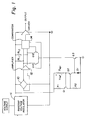
- FIGURE 1 A diagrammatic representation of a bipolar circuit employing the principles of the invention is shown in FIGURE 1.
- a constant bias voltage which is independent of temperature is supplied to a Hall effect device 10 by a bandgap voltage regulator 11 from an external voltage supply.
- the output of Hall element 10 in response to a magnetic field is amplified by a constant gain amplifier and thus appears across load resistors RL 1 and RL 2 .
- FIGURE 1 is a bipolar latch circuit which turns on (operates) at a predetermined magnitude and direction of magnetic field and turns off (releases) at the same magnitude but opposite direction of magnetic field.
- a differential transistor switch (not shown) is used to change the comparator threshold polarity and alternately switches transistors Q10 and Q12 on and off to switch a reference current (I ref ) on the collector of Q10 or Q12, respectively, to load resistors RL 1 or RL 2 , respectively.
- the reference current (I ref ) is determined by a current mirror circuit comprising transistors Q1, Q2 and Q3; resistors R1, R2 and R epi and diode D1. It will be recognized that by appropriate selection of the values of resistors R1 and R2, the current (or any function thereof) passing through resistor R epi appears as the current (I ref ) on the collector of transistor Q3.
- the circuit of FIGURE 1 is a bipolar latch circuit designed to operate at a given magnetic threshold irrespective of temperature changes.
- resistor R epi is fabricated to the same epitaxial layer in which the Hall element is formed so that the mobility of electrons therein matches the drift mobility of the Hall element.
- the resistance of R epi may be expressed as:
- B op 1 S H A V V ref RL R epi
- V ref V ref RL
- V ref V ref RL
- R epi constant R epi
- the entire circuit can be formed on the same chip on which the Hall element is formed by relatively simply masking and diffusion techniques. Furthermore, the same masking and diffusion techniques which are used to ordinarily form the amplifier circuit will be used to form the additional components required for the temperature compensation circuit. Thus the effects of temperature change will be canceled and the need for a temperature independent resistor is totally eliminated.
- resistors R1 and R2 can be made selectively variable by conventional trimming techniques.
- the values of resistors R1 and R2 can be selectively adjusted to provide a circuit in which the Hall effect sensitivity can increase with temperature, decrease with temperature, or be maintained relatively constant with temperature changes.
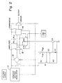
- FIGURE 2 An alternative embodiment of the invention is illustrated in FIGURE 2 wherein the same principles are applied to provide unipolar operation so that the latching circuit turns on (operates) at a predetermined magnitude and direction of magnetic field and turns off (releases) at a predetermined lesser magnitude of the same direction of magnetic field.
- the current I ref on the collector of transistor Q3 is applied directly to load resistor RL 1 .
- transistor Q12 When transistor Q12 is turned on, a fractional portion which is proportional to the desired switching hysteresis is applied to resistor RL 2 .
- the entire circuitry for either unipolar or bipolar operation can be included in the manufacturing process and the desired operational configuration selected by convention interconnection selection techniques.
Landscapes
- Physics & Mathematics (AREA)
- General Physics & Mathematics (AREA)
- Condensed Matter Physics & Semiconductors (AREA)
- Hall/Mr Elements (AREA)
- Measuring Magnetic Variables (AREA)
Claims (4)
- Circuit destiné à produire une sortie compensée en température pour un élément à effet de Hall (10) formé dans une couche épitaxiale de matériau, le circuit comprenant:(a) une résistance de charge sensible à la température (RL1) entre la source de tension de polarisation de l'élément de Hall et une sortie de l'élément de Hall; et(b) un moyen formant circuit miroir de courant (Q1, Q2, Q3, R1, R2, Repi, D1), le circuit étant en outre caractérisé par:(c) une résistance de référence sensible (Repi) à la température produisant une tension de référence sensible à la température qui est inversement proportionnelle à la résistance de la résistance de charge sensible à la température; et par(d) ledit moyen formant circuit miroir de courant (Q1, Q2, Q3, R1, R2, Repi, D1) produisant un courant proportionnel au courant passant à travers la résistance de référence sensible à la température (Repi) vers la résistance de charge sensible à la température (RL1), de manière que la tension à travers la résistance de charge sensible à la température varie avec la température en relation directe avec la sensibilité de l'élément à effet de Hall.
- Circuit selon la revendication 1, caractérisé en ce que ladite résistance de référence (Repi) est formée dans la même couche épitaxiale de matériau dans laquelle est formé l'élément de Hall.
- Circuit selon les revendications 1 ou 2, caractérisé par:(e) une seconde résistance de charge sensible à la température (RL2) entre source de la tension de polarisation de l'élément de Hall et une seconde sortie d'élément de Hall; et(f) un moyen destiné à commuter en alternance de manière sélective le courant proportionnel au courant passant à travers la résistance de référence (Repi) vers ladite résistance de charge sensible à la température (RL1) et ladite seconde résistance de charge sensible à la température (RL2).
- Circuit selon les revendications 1 ou 2, caractérisé par:(e) une seconde résistance de charge sensible à la température (RL2) entre la source de tension de polarisation de l'élément de Hall et une seconde sortie d'élément de Hall; et(f) un moyen destiné à commuter de manière sélective un courant proportionnel au courant passant à travers la résistance de référence (Repi) vers ladite seconde résistance de charge sensible à la température (RL2).
Applications Claiming Priority (2)
| Application Number | Priority Date | Filing Date | Title |
|---|---|---|---|
| US505710 | 1990-04-05 | ||
| US07/505,710 US5055768A (en) | 1990-04-05 | 1990-04-05 | Temperature compensator for hall effect circuit |
Publications (3)
| Publication Number | Publication Date |
|---|---|
| EP0450910A2 EP0450910A2 (fr) | 1991-10-09 |
| EP0450910A3 EP0450910A3 (en) | 1993-03-17 |
| EP0450910B1 true EP0450910B1 (fr) | 1997-01-08 |
Family
ID=24011502
Family Applications (1)
| Application Number | Title | Priority Date | Filing Date |
|---|---|---|---|
| EP91302871A Expired - Lifetime EP0450910B1 (fr) | 1990-04-05 | 1991-04-02 | Circuit de compensation de la température pour un élément à effet de Hall |
Country Status (3)
| Country | Link |
|---|---|
| US (1) | US5055768A (fr) |
| EP (1) | EP0450910B1 (fr) |
| DE (1) | DE69123993T2 (fr) |
Families Citing this family (25)
| Publication number | Priority date | Publication date | Assignee | Title |
|---|---|---|---|---|
| DE59109002D1 (de) * | 1991-07-31 | 1998-07-09 | Micronas Intermetall Gmbh | Hallsensor mit Selbstkompensation |
| US5402064A (en) * | 1992-09-02 | 1995-03-28 | Santa Barbara Research Center | Magnetoresistive sensor circuit with high output voltage swing and temperature compensation |
| US5444369A (en) * | 1993-02-18 | 1995-08-22 | Kearney-National, Inc. | Magnetic rotational position sensor with improved output linearity |
| US5455510A (en) * | 1994-03-11 | 1995-10-03 | Honeywell Inc. | Signal comparison circuit with temperature compensation |
| US6104231A (en) * | 1994-07-19 | 2000-08-15 | Honeywell International Inc. | Temperature compensation circuit for a hall effect element |
| DE4431703C2 (de) * | 1994-09-06 | 1997-01-30 | Itt Ind Gmbh Deutsche | Magnetfeldsensor mit Hallelement |
| US5488296A (en) * | 1995-01-25 | 1996-01-30 | Honeywell Inc. | Temperature compensated magnetically sensitive circuit |
| US5497084A (en) * | 1995-03-03 | 1996-03-05 | Honeywell Inc. | Geartooth sensor with means for selecting a threshold magnitude as a function of the average and minimum values of a signal of magnetic field strength |
| JPH0968403A (ja) * | 1995-08-31 | 1997-03-11 | Denso Corp | スロットルバルブ開度センサ |
| US5694040A (en) * | 1996-07-02 | 1997-12-02 | Honeywell Inc. | Magnetic sensor circuit with two magnetically sensitive devices |
| US6404188B1 (en) | 1998-03-19 | 2002-06-11 | Honeywell Inc | Single geartooth sensor yielding multiple output pulse trains |
| DE19858868C2 (de) * | 1998-12-19 | 2003-06-18 | Micronas Gmbh | Hallsensor |
| DE19951817A1 (de) * | 1999-10-27 | 2001-05-23 | Micronas Gmbh | Zwei-Draht-Sensoranordnung |
| DE10032527C1 (de) * | 2000-07-05 | 2001-12-06 | Infineon Technologies Ag | Temperaturkompensationsschaltung für ein Hall-Element |
| GB2365130B (en) | 2000-07-20 | 2005-01-19 | Honeywell Control Syst | Improved proximity sensor and related methods |
| US6879145B1 (en) | 2002-02-15 | 2005-04-12 | Larry L. Harris | Voltage isolation buffer with hall effect magnetic field sensor |
| US7265539B2 (en) * | 2005-06-09 | 2007-09-04 | Ford Motor Company | Calibration of a hall effect sensor |
| US8421427B2 (en) * | 2007-09-07 | 2013-04-16 | Oki Data Corporation | Reference voltage generation circuit, drive circuit, light emitting diode head, and image forming apparatus |
| US9013167B2 (en) * | 2010-11-09 | 2015-04-21 | Texas Instruments Incorporated | Hall effect device having voltage based biasing for temperature compensation |
| JP5800152B2 (ja) * | 2012-10-24 | 2015-10-28 | Tdk株式会社 | 磁気センサ |
| US9063174B2 (en) | 2012-11-14 | 2015-06-23 | Olympus Scientific Solutions Americas Inc. | Hall effect measurement instrument with temperature compensation |
| CN103825591B (zh) * | 2014-03-13 | 2016-08-17 | 北京经纬恒润科技有限公司 | 一种开关型霍尔芯片 |
| JP2017032278A (ja) * | 2015-07-28 | 2017-02-09 | エスアイアイ・セミコンダクタ株式会社 | センサ装置 |
| US10162017B2 (en) * | 2016-07-12 | 2018-12-25 | Allegro Microsystems, Llc | Systems and methods for reducing high order hall plate sensitivity temperature coefficients |
| IT201700071189A1 (it) * | 2017-06-26 | 2018-12-26 | St Microelectronics Srl | Circuito di compensazione in temperatura, dispositivo e procedimento corrispondenti |
Family Cites Families (7)
| Publication number | Priority date | Publication date | Assignee | Title |
|---|---|---|---|---|
| US3816766A (en) * | 1973-01-29 | 1974-06-11 | Sprague Electric Co | Integrated circuit with hall cell |
| CA1088159A (fr) * | 1977-01-03 | 1980-10-21 | Wilson D. Pace | Commutateur de circuit integre a effet de hall |
| US4521727A (en) * | 1983-05-23 | 1985-06-04 | Honeywell Inc. | Hall effect circuit with temperature compensation |
| US4833406A (en) * | 1986-04-17 | 1989-05-23 | Household Commercial Financial Services Inc. | Temperature compensated Hall-effect sensor apparatus |
| US4734594A (en) * | 1986-12-31 | 1988-03-29 | Honeywell Inc. | Offset correction for sensor with temperature dependent sensitivity |
| US4760285A (en) * | 1987-03-30 | 1988-07-26 | Honeywell Inc. | Hall effect device with epitaxal layer resistive means for providing temperature independent sensitivity |
| US4908527A (en) * | 1988-09-08 | 1990-03-13 | Xolox Corporation | Hall-type transducing device |
-
1990
- 1990-04-05 US US07/505,710 patent/US5055768A/en not_active Expired - Lifetime
-
1991
- 1991-04-02 EP EP91302871A patent/EP0450910B1/fr not_active Expired - Lifetime
- 1991-04-02 DE DE69123993T patent/DE69123993T2/de not_active Expired - Fee Related
Also Published As
| Publication number | Publication date |
|---|---|
| EP0450910A2 (fr) | 1991-10-09 |
| DE69123993D1 (de) | 1997-02-20 |
| EP0450910A3 (en) | 1993-03-17 |
| DE69123993T2 (de) | 1997-07-10 |
| US5055768A (en) | 1991-10-08 |
Similar Documents
| Publication | Publication Date | Title |
|---|---|---|
| EP0450910B1 (fr) | Circuit de compensation de la température pour un élément à effet de Hall | |
| EP0285016B1 (fr) | Dispositif à effet de Hall | |
| US4792748A (en) | Two-terminal temperature-compensated current source circuit | |
| US6937001B2 (en) | Circuit for generating a reference voltage having low temperature dependency | |
| US5559500A (en) | Overcurrent sense circuit | |
| US5795069A (en) | Temperature sensor and method | |
| US4521727A (en) | Hall effect circuit with temperature compensation | |
| US5877617A (en) | Load current supply circuit having current sensing function | |
| GB2071946A (en) | Temperature detecting device | |
| EP0771424A1 (fr) | Circuit de compensation thermique pour element a effet de hall | |
| EP0610494B1 (fr) | Capteur magnetoresistif a circuit a excursion de tension de sortie eleve et la compensation de temperature | |
| JPH06289111A (ja) | ホール素子の駆動回路 | |
| CA1147805A (fr) | Bloc a compensation pour l'alimentation en courant | |
| JPH0210269A (ja) | 電流測定回路 | |
| GB1587870A (en) | Hall-effect integrated circuit | |
| US4734594A (en) | Offset correction for sensor with temperature dependent sensitivity | |
| EP0104770B1 (fr) | Circuit générant une tension dépendant de la température | |
| GB2093303A (en) | Voltage sensing circuit | |
| US7038447B2 (en) | Sensor circuit and method of producing it | |
| US4683429A (en) | Electrical circuit which is linearly responsive to changes in magnetic field intensity | |
| EP3422032A1 (fr) | Circuit de compensation de température, dispositif et procédé correspondants | |
| EP0024151B1 (fr) | Dispositif de commande de la vitesse d'un moteur à courant continu | |
| US3430076A (en) | Temperature compensated bias circuit | |
| US6810745B2 (en) | Temperature dependent sensitivity compensation structure of sensor | |
| JP3049843B2 (ja) | 抵抗体電極構造の形成方法 |
Legal Events
| Date | Code | Title | Description |
|---|---|---|---|
| PUAI | Public reference made under article 153(3) epc to a published international application that has entered the european phase |
Free format text: ORIGINAL CODE: 0009012 |
|
| AK | Designated contracting states |
Kind code of ref document: A2 Designated state(s): DE FR GB IT NL |
|
| PUAL | Search report despatched |
Free format text: ORIGINAL CODE: 0009013 |
|
| AK | Designated contracting states |
Kind code of ref document: A3 Designated state(s): DE FR GB IT NL |
|
| 17P | Request for examination filed |
Effective date: 19931118 |
|
| 17Q | First examination report despatched |
Effective date: 19950221 |
|
| GRAG | Despatch of communication of intention to grant |
Free format text: ORIGINAL CODE: EPIDOS AGRA |
|
| GRAH | Despatch of communication of intention to grant a patent |
Free format text: ORIGINAL CODE: EPIDOS IGRA |
|
| GRAH | Despatch of communication of intention to grant a patent |
Free format text: ORIGINAL CODE: EPIDOS IGRA |
|
| GRAA | (expected) grant |
Free format text: ORIGINAL CODE: 0009210 |
|
| AK | Designated contracting states |
Kind code of ref document: B1 Designated state(s): DE FR GB IT NL |
|
| PG25 | Lapsed in a contracting state [announced via postgrant information from national office to epo] |
Ref country code: IT Free format text: LAPSE BECAUSE OF FAILURE TO SUBMIT A TRANSLATION OF THE DESCRIPTION OR TO PAY THE FEE WITHIN THE PRE;WARNING: LAPSES OF ITALIAN PATENTS WITH EFFECTIVE DATE BEFORE 2007 MAY HAVE OCCURRED AT ANY TIME BEFORE 2007. THE CORRECT EFFECTIVE DATE MAY BE DIFFERENT FROM THE ONE RECORDED.SCRIBED TIME-LIMIT Effective date: 19970108 Ref country code: NL Free format text: LAPSE BECAUSE OF FAILURE TO SUBMIT A TRANSLATION OF THE DESCRIPTION OR TO PAY THE FEE WITHIN THE PRESCRIBED TIME-LIMIT Effective date: 19970108 |
|
| ET | Fr: translation filed | ||
| REF | Corresponds to: |
Ref document number: 69123993 Country of ref document: DE Date of ref document: 19970220 |
|
| NLV1 | Nl: lapsed or annulled due to failure to fulfill the requirements of art. 29p and 29m of the patents act | ||
| PLBE | No opposition filed within time limit |
Free format text: ORIGINAL CODE: 0009261 |
|
| STAA | Information on the status of an ep patent application or granted ep patent |
Free format text: STATUS: NO OPPOSITION FILED WITHIN TIME LIMIT |
|
| 26N | No opposition filed | ||
| REG | Reference to a national code |
Ref country code: GB Ref legal event code: IF02 |
|
| PGFP | Annual fee paid to national office [announced via postgrant information from national office to epo] |
Ref country code: GB Payment date: 20080317 Year of fee payment: 18 |
|
| PGFP | Annual fee paid to national office [announced via postgrant information from national office to epo] |
Ref country code: DE Payment date: 20080430 Year of fee payment: 18 |
|
| PGFP | Annual fee paid to national office [announced via postgrant information from national office to epo] |
Ref country code: FR Payment date: 20080403 Year of fee payment: 18 |
|
| GBPC | Gb: european patent ceased through non-payment of renewal fee |
Effective date: 20090402 |
|
| REG | Reference to a national code |
Ref country code: FR Ref legal event code: ST Effective date: 20091231 |
|
| PG25 | Lapsed in a contracting state [announced via postgrant information from national office to epo] |
Ref country code: DE Free format text: LAPSE BECAUSE OF NON-PAYMENT OF DUE FEES Effective date: 20091103 |
|
| PG25 | Lapsed in a contracting state [announced via postgrant information from national office to epo] |
Ref country code: FR Free format text: LAPSE BECAUSE OF NON-PAYMENT OF DUE FEES Effective date: 20091222 Ref country code: GB Free format text: LAPSE BECAUSE OF NON-PAYMENT OF DUE FEES Effective date: 20090402 |