EP0451454A2 - Semiconductor device having element regions being electrically isolated from each other - Google Patents
Semiconductor device having element regions being electrically isolated from each other Download PDFInfo
- Publication number
- EP0451454A2 EP0451454A2 EP91101759A EP91101759A EP0451454A2 EP 0451454 A2 EP0451454 A2 EP 0451454A2 EP 91101759 A EP91101759 A EP 91101759A EP 91101759 A EP91101759 A EP 91101759A EP 0451454 A2 EP0451454 A2 EP 0451454A2
- Authority
- EP
- European Patent Office
- Prior art keywords
- semiconductor device
- grooves
- element isolation
- element regions
- surrounding
- Prior art date
- Legal status (The legal status is an assumption and is not a legal conclusion. Google has not performed a legal analysis and makes no representation as to the accuracy of the status listed.)
- Granted
Links
Images

Classifications
-
- H—ELECTRICITY
- H10—SEMICONDUCTOR DEVICES; ELECTRIC SOLID-STATE DEVICES NOT OTHERWISE PROVIDED FOR
- H10P—GENERIC PROCESSES OR APPARATUS FOR THE MANUFACTURE OR TREATMENT OF DEVICES COVERED BY CLASS H10
- H10P90/00—Preparation of wafers not covered by a single main group of this subclass, e.g. wafer reinforcement
- H10P90/19—Preparing inhomogeneous wafers
- H10P90/1904—Preparing vertically inhomogeneous wafers
- H10P90/1906—Preparing SOI wafers
-
- H—ELECTRICITY
- H10—SEMICONDUCTOR DEVICES; ELECTRIC SOLID-STATE DEVICES NOT OTHERWISE PROVIDED FOR
- H10W—GENERIC PACKAGES, INTERCONNECTIONS, CONNECTORS OR OTHER CONSTRUCTIONAL DETAILS OF DEVICES COVERED BY CLASS H10
- H10W10/00—Isolation regions in semiconductor bodies between components of integrated devices
- H10W10/01—Manufacture or treatment
- H10W10/011—Manufacture or treatment of isolation regions comprising dielectric materials
- H10W10/014—Manufacture or treatment of isolation regions comprising dielectric materials using trench refilling with dielectric materials, e.g. shallow trench isolations
- H10W10/0145—Manufacture or treatment of isolation regions comprising dielectric materials using trench refilling with dielectric materials, e.g. shallow trench isolations of trenches having shapes other than rectangular or V-shape
- H10W10/0147—Manufacture or treatment of isolation regions comprising dielectric materials using trench refilling with dielectric materials, e.g. shallow trench isolations of trenches having shapes other than rectangular or V-shape the shapes being altered by a local oxidation of silicon process, e.g. trench corner rounding by LOCOS
-
- H—ELECTRICITY
- H10—SEMICONDUCTOR DEVICES; ELECTRIC SOLID-STATE DEVICES NOT OTHERWISE PROVIDED FOR
- H10W—GENERIC PACKAGES, INTERCONNECTIONS, CONNECTORS OR OTHER CONSTRUCTIONAL DETAILS OF DEVICES COVERED BY CLASS H10
- H10W10/00—Isolation regions in semiconductor bodies between components of integrated devices
- H10W10/01—Manufacture or treatment
- H10W10/061—Manufacture or treatment using SOI processes together with lateral isolation, e.g. combinations of SOI and shallow trench isolations
-
- H—ELECTRICITY
- H10—SEMICONDUCTOR DEVICES; ELECTRIC SOLID-STATE DEVICES NOT OTHERWISE PROVIDED FOR
- H10W—GENERIC PACKAGES, INTERCONNECTIONS, CONNECTORS OR OTHER CONSTRUCTIONAL DETAILS OF DEVICES COVERED BY CLASS H10
- H10W10/00—Isolation regions in semiconductor bodies between components of integrated devices
- H10W10/10—Isolation regions comprising dielectric materials
- H10W10/17—Isolation regions comprising dielectric materials formed using trench refilling with dielectric materials, e.g. shallow trench isolations
-
- H—ELECTRICITY
- H10—SEMICONDUCTOR DEVICES; ELECTRIC SOLID-STATE DEVICES NOT OTHERWISE PROVIDED FOR
- H10W—GENERIC PACKAGES, INTERCONNECTIONS, CONNECTORS OR OTHER CONSTRUCTIONAL DETAILS OF DEVICES COVERED BY CLASS H10
- H10W10/00—Isolation regions in semiconductor bodies between components of integrated devices
- H10W10/10—Isolation regions comprising dielectric materials
- H10W10/181—Semiconductor-on-insulator [SOI] isolation regions, e.g. buried oxide regions of SOI wafers
-
- H—ELECTRICITY
- H10—SEMICONDUCTOR DEVICES; ELECTRIC SOLID-STATE DEVICES NOT OTHERWISE PROVIDED FOR
- H10W—GENERIC PACKAGES, INTERCONNECTIONS, CONNECTORS OR OTHER CONSTRUCTIONAL DETAILS OF DEVICES COVERED BY CLASS H10
- H10W10/00—Isolation regions in semiconductor bodies between components of integrated devices
- H10W10/01—Manufacture or treatment
- H10W10/041—Manufacture or treatment of isolation regions comprising polycrystalline semiconductor materials
-
- H—ELECTRICITY
- H10—SEMICONDUCTOR DEVICES; ELECTRIC SOLID-STATE DEVICES NOT OTHERWISE PROVIDED FOR
- H10W—GENERIC PACKAGES, INTERCONNECTIONS, CONNECTORS OR OTHER CONSTRUCTIONAL DETAILS OF DEVICES COVERED BY CLASS H10
- H10W10/00—Isolation regions in semiconductor bodies between components of integrated devices
- H10W10/40—Isolation regions comprising polycrystalline semiconductor materials
Definitions
- This invention relates to the improvement of a semiconductor device, and more particularly to the improvement of a technique for isolation between element regions.
- a semiconductor device of this invention in which a distance between a groove surrounding an element region and a groove surrounding another element region is set at least 3 ⁇ m so as to electrically isolate the former element region from the latter adjacent element region.
Landscapes
- Element Separation (AREA)
- Bipolar Integrated Circuits (AREA)
- Bipolar Transistors (AREA)
Abstract
Description
- This invention relates to the improvement of a semiconductor device, and more particularly to the improvement of a technique for isolation between element regions.
- In general, in a semiconductor integrated circuit, a plurality of element regions which are electrically isolated from one another are formed in the main surface of a semiconductor substrate and active elements and passive elements are formed in the element regions.
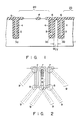
- As a method of isolating the element regions from one another an isolation technique using PN junctions, an isolation technique using oxide films and an isolation technique using grooves are known. The conventional semiconductor device and the method for manufacturing the same are explained below by using the isolation technique using the oxide films as an example. Fig. 1 shows the conventional semiconductor integrated circuit in which the isolation technique using the oxide films is used.
- In a
silicon substrate 1,element regions 2a, 2b, ... are formed. Theelement regions 2a, 2b, ... are surrounded bygrooves oxide film 4 is formed on the field region and the internal surfaces of thegrooves Polysilicon layers 5 are buried in thegrooves oxide film 4 is formed. Thincap oxide films 6 are formed on thegrooves polysilicon layers 5 are buried. - The element isolation in the above semiconductor integrated circuit is effected as follows.
- First, the
grooves element regions 2 are formed in thesilicon substrate 1 by an anisotropic etching technique. Then, a non-oxide film (Si₃N₄) such as a nitride film is formed on theelement regions 2. After this, theoxide film 4 is formed on the field region and the internal surfaces of thegrooves oxide film 4, thepolysilicon layers 5 are buried in thegrooves polysilicon layers 5 are made flat and then the thincap oxide films 6 are formed on the grooves. - In the integrated circuit thus formed, a distance WTT between the side wall of the
groove 3a and the side wall of thegroove 3b is designed to a minimum possible length in order to enhance the integration density of the elements. - However, it is generally known that as the distance between the grooves becomes shorter, thermal stress is more concentrated on the corner portions of the
grooves oxide films 4 on the field region and the internal surfaces of thegrooves dislocation defects 9 may be caused in theupper corner portions 7 and bottom corner portions 8 because of the concentration of thermal stress at the time of oxidation. Thedislocation defects 9 increase leak current between the collectors of transistors formed in the silicon substrate. Further, the transistor characteristic such as the IC (collector current)-hFE (grounded emitter current amplification factor) characteristic will be deteriorated. That is, if thedislocation defects 9 occur at a certain density, recombination current around the defect increases to deteriorate the element characteristic and element isolation characteristic, making the semiconductor device definitely impractical. - This invention has been made to solve the above problems, and an object of this invention is to provide a semiconductor device in which occurrence of dislocation defects in the upper and bottom corner portions of the element isolation grooves can be suppressed and deterioration of the element characteristic and the element isolation characteristic can be prevented.
- In order to attain the above object, there is provided a semiconductor device of this invention in which a distance between a groove surrounding an element region and a groove surrounding another element region is set at least 3 µm so as to electrically isolate the former element region from the latter adjacent element region.
- This invention can be more fully understood from the following detailed description when taken in conjunction with the accompanying drawings, in which:
- Figs. 1 and 2 are cross sectional views each showing the conventional semiconductor device;
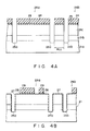
- Fig. 3 is a perspective view showing a semiconductor device according to one embodiment of this invention;
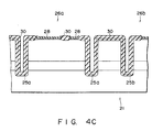
- Figs. 4A to 4C are cross sectional views showing a method of manufacturing the semiconductor device shown in Fig. 3;
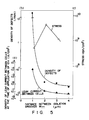
- Fig. 5 is a characteristic diagram showing the characteristic of the semiconductor device of this invention; and
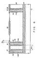
- Fig. 6 is a cross sectional view showing a semiconductor device according to another embodiment of this invention.
- Now, a semiconductor device according to one embodiment of this invention and a method for manufacturing the same are explained in detail with reference to the accompanying drawings.
- Fig. 3 shows a semiconductor device according to one embodiment of this invention. The semiconductor device has bipolar transistor arrays formed in element regions. That is, an N⁺-type buried
layer 12 is formed on a P-type monocrystalline silicon substrate 11. N-typeepitaxial layers 13 are formed on the N⁺-type buriedlayer 12.Element isolation grooves element regions 14a, 14b, ... are formed in the silicon substrate 11 and N-typeepitaxial layers 13. P⁺-type impurity regions 16 are formed on the bottom portions of theelement isolation grooves oxide film 17 is formed on a field region and the internal surfaces of theelement isolation grooves Polysilicon layers 18 are buried in theelement isolation grooves oxide film 17 is formed. Thincap oxide films 19 are formed on thegrooves polysilicon layers 18 are buried. Further, an N⁺-type collector lead-outregion 20, P-type base region 21 and N⁺-type emitter region 22 are formed in the N-type epitaxial regions of theelement regions 14a, 14b, ... - In the above semiconductor device, a WTT distance between the
adjacent element regions element isolation grooves oxide film 17 having a film thickness of not larger than 0.9 µm (9000 Å) is formed on the internal surfaces of theelement isolation regions - With the above construction, occurrence of dislocation defects in the upper corner and bottom corner of the element isolation region can be suppressed and therefore the element characteristic and element isolation characteristic will not be deteriorated.
- Figs. 4A to 4C show a method of manufacturing the semiconductor device shown in Fig. 3.
- First, as shown in Fig. 4A, an
SiO₂ film 21 is formed on the main surface of amonocrystalline silicon substrate 21 formed of a P-type substrate 21a, N⁺-type buriedlayer 21b and N-typeepitaxial layer 21c by use of a CVD method or thermal oxidation method. Further, aresist pattern 24 is formed on theSiO₂ film 23. After this, themonocrystalline silicon substrate 21 is etched in a vertical direction by use of an RIE (reactive ion etching) method so as to formelement isolation grooves element isolation grooves element regions 26a, 26b ..., and theelement isolation grooves - Next, as shown in Fig. 4B, the
SiO₂ film 23 andresist pattern 24 are removed. After this, thermal oxidation is effected in an H₂ and O₂ gas atmosphere at a temperature of approx. 950 Å to form anSiO₂ film 27 having a film thickness of approx. 500 Å. Further, anSi₃N₄ film 28 having a film thickness of approx. 1000 Å is formed by deposition at a temperature of approx. 780°C by use of an LP-CVD method. Then, aresist pattern 29 is formed on theSi₃N₄ film 28 by a photo-etching technique. Next, theSi₃N₄ film 28 is selectively etched by a plasma-etching technique to leave the Si₃N₄ film (non-oxide film) 28 only in positions above theelement regions 26a, 26b, ... - Next, as shown in Fig. 4C, the
resist pattern 29 is removed. After this, wet oxidation is effected at a temperature of approx. 1000 Å with theSi₃N₄ film 28 used as a mask. As a result, anoxide film 30 having a film thickness of less than 9000 Å, for example, 8000 Å is formed on the field region and on the internal surface of theelement isolation grooves - After this, polysilicon layers are buried into the
element isolation grooves element isolation grooves element regions 26a, 26b, ... - Now, the characteristic of the semiconductor device of this invention is explained with reference to Fig. 5.
- Bipolar transistor arrays were formed with a distance WTT between the side wall of one of the element isolation grooves and the side wall of an adjacent one of the element isolation grooves used as parameter. The distance WTT was set at four different values of 1.0, 2.0, 3.0 and 4.0 µm. The film thickness of the field oxide film was set at approx. 9000 Å and a distance WTL between the
element isolation grooves - The defects occurring in the upper corners and bottom corners of the
element isolation grooves element isolation grooves - The defects were evaluated by etching off the entire substrate surface after the step of forming the elements and then effecting the Wright etching to selectively etch the defects. After this, the number of defects were counted by observation of the defects by use of an optical microscope and were expressed by the density of defects occurring for the length of 1 mm of the
element isolation grooves element isolation grooves element isolation grooves - In Fig. 5 in which the evaluated items are collectively shown, the abscissa indicates the distance WTT (µm) between the adjacent element isolation grooves, the ordinate (a) indicates the density (A/cm²) of leak current flowing between the cells when a voltage of 12 V is applied between the elements, the ordinate (b) indicates the density of defects (/mm) in the upper corner and bottom corner, and the ordinate (c) indicates the stress (dyn/cm²).
- That is, when the distance WTT (µm) between the adjacent element isolation grooves is sequentially set to 4.0 m, 3.0 µm, 2.0 µm and 1.0 µm in this order, the stress basically increases and at the same time the defect density increases. The reason why the stress decreases near the point of 1.0 µm is that a large umber of defects are caused by application of an extremely strong stress to reduce the stress. Further, as the distance WTT decreases, the density of leak current between the cells indicating the element isolation characteristic increases. As a result, it is proved that it is preferable to set the distance WTT between the adjacent
element isolation grooves - Fig. 6 shows a semiconductor device according to another embodiment of this invention.
- The semiconductor device uses a bonded wafer or SOI wafer as a substrate. That is, an
oxide film 42 is formed on amonocrystalline silicon substrate 41. Further, amonocrystalline silicon substrate 43 is formed on theoxide film 42. Themonocrystalline silicon substrate 43 is polished to have a sufficiently small thickness, for example, a thickness of approx. 5 µm after it is bonded with thesubstrate 41. Element isolation grooves 44a, 44b, ... are formed in themonocrystalline silicon substrate 43.Oxide films 45 are formed on the field region and the internal surface of the element isolation grooves 44a, 44b, ... Polysilicon layers 46 are buried in the element isolation grooves 44a, 44b, ... on which theoxide films 45 are formed. Thincap oxide films 47 are formed on the element isolation grooves 44a, 44b, ... in which the polysilicon layers 46 are buried. - The distance WTT between the adjacent element isolation grooves 44a, 44b, ... is set to at least 3.0 µm. Further, the
oxide films 46 having a film thickness of not more than 0.9 µm (9000 Å) are formed on the internal surfaces of the element isolation grooves 44a, 44b, ... having a width in the range of 1 to 2 µm. - With the above construction, occurrence of the dislocation defects in the upper corner and bottom corner of the element isolation groove can be suppressed, and at the same time, the element characteristic and element isolation characteristic will not be deteriorated.
- Reference signs in the claims are intended for better understanding and shall not limit the scope.
Claims (7)
- A semiconductor device in which one element region (14a) is electrically isolated from another element region (14b) adjacent thereto by forming a groove (15a) surrounding said one element region (14a), characterized in that a distance between said groove (15a) surrounding said one element region (14a) and a groove (15b) surrounding said another element region (14b) is set to be equal to or larger than 3 µm.
- A semiconductor device according to claim 1, characterized in that an oxide film (17) having a film thickness of not larger than 9000 Å is formed in each of said grooves surrounding said one and another element regions.
- A semiconductor device according to claim 1, characterized in that the width of each of said grooves surrounding said one and another element regions is set to 1 to 2 µm.
- A semiconductor device according to claim 1, characterized in that said one and another element regions are formed in a bonded wafer.
- A semiconductor device according to claim 1, characterized in that said one and another element regions are formed in an SOI wafer.
- A semiconductor device according to claim 1, characterized in that bipolar transistors are formed in said one and another element regions.
- A semiconductor device according to claim 1, characterized in that a polysilicon layer (18) is buried in each of said grooves surrounding said one and another element regions.
Applications Claiming Priority (3)
| Application Number | Priority Date | Filing Date | Title |
|---|---|---|---|
| JP30584/90 | 1990-02-09 | ||
| JP2030584A JPH0736419B2 (en) | 1990-02-09 | 1990-02-09 | Semiconductor device and manufacturing method thereof |
| JP3058490 | 1990-02-09 |
Publications (3)
| Publication Number | Publication Date |
|---|---|
| EP0451454A2 true EP0451454A2 (en) | 1991-10-16 |
| EP0451454A3 EP0451454A3 (en) | 1994-08-24 |
| EP0451454B1 EP0451454B1 (en) | 2002-05-15 |
Family
ID=12307908
Family Applications (1)
| Application Number | Title | Priority Date | Filing Date |
|---|---|---|---|
| EP91101759A Expired - Lifetime EP0451454B1 (en) | 1990-02-09 | 1991-02-08 | Process of fabrication of a semiconductor device having element regions being electrically isolated from each other |
Country Status (5)
| Country | Link |
|---|---|
| US (1) | US5111272A (en) |
| EP (1) | EP0451454B1 (en) |
| JP (1) | JPH0736419B2 (en) |
| KR (1) | KR940003217B1 (en) |
| DE (1) | DE69133009T2 (en) |
Cited By (4)
| Publication number | Priority date | Publication date | Assignee | Title |
|---|---|---|---|---|
| EP0735594A3 (en) * | 1995-03-30 | 1997-01-08 | Toshiba Kk | Semiconductor devices on insulator and manufacturing method |
| EP0653785A3 (en) * | 1993-11-17 | 1997-07-09 | Nippon Denso Co | Di-electric isolated type semiconductor device. |
| GB2322736A (en) * | 1997-02-28 | 1998-09-02 | Int Rectifier Corp | Forming trench isolation regions in integrated circuits |
| EP1220312A1 (en) * | 2000-12-29 | 2002-07-03 | STMicroelectronics S.r.l. | Integration process on a SOI substrate of a semiconductor device comprising at least a dielectrically isolated well |
Families Citing this family (6)
| Publication number | Priority date | Publication date | Assignee | Title |
|---|---|---|---|---|
| JPH04107949A (en) * | 1990-08-28 | 1992-04-09 | Mitsubishi Electric Corp | Semiconductor device and its manufacture |
| EP0608999B1 (en) * | 1993-01-29 | 1997-03-26 | National Semiconductor Corporation | Bipolar transistors and methods for fabrication thereof |
| JP3031137B2 (en) * | 1993-10-15 | 2000-04-10 | 株式会社デンソー | Insulator-isolated semiconductor device |
| US5693971A (en) * | 1994-07-14 | 1997-12-02 | Micron Technology, Inc. | Combined trench and field isolation structure for semiconductor devices |
| JP4657614B2 (en) * | 2004-03-09 | 2011-03-23 | Okiセミコンダクタ株式会社 | Semiconductor device and manufacturing method of semiconductor device |
| JP7038518B2 (en) * | 2017-10-11 | 2022-03-18 | ローム株式会社 | Semiconductor device |
Family Cites Families (7)
| Publication number | Priority date | Publication date | Assignee | Title |
|---|---|---|---|---|
| US4238278A (en) * | 1979-06-14 | 1980-12-09 | International Business Machines Corporation | Polycrystalline silicon oxidation method for making shallow and deep isolation trenches |
| JPS5943545A (en) * | 1982-09-06 | 1984-03-10 | Hitachi Ltd | Semiconductor ic device and its manufacture |
| US4593459A (en) * | 1984-12-28 | 1986-06-10 | Gte Laboratories Incorporated | Monolithic integrated circuit structure and method of fabrication |
| US4631803A (en) * | 1985-02-14 | 1986-12-30 | Texas Instruments Incorporated | Method of fabricating defect free trench isolation devices |
| US4799099A (en) * | 1986-01-30 | 1989-01-17 | Texas Instruments Incorporated | Bipolar transistor in isolation well with angled corners |
| JPS63314844A (en) * | 1987-06-18 | 1988-12-22 | Toshiba Corp | Manufacture of semiconductor device |
| JP2839651B2 (en) * | 1989-06-14 | 1998-12-16 | 株式会社東芝 | Semiconductor device manufacturing method and semiconductor device |
-
1990
- 1990-02-09 JP JP2030584A patent/JPH0736419B2/en not_active Expired - Lifetime
-
1991
- 1991-02-07 US US07/651,988 patent/US5111272A/en not_active Expired - Lifetime
- 1991-02-08 DE DE69133009T patent/DE69133009T2/en not_active Expired - Fee Related
- 1991-02-08 EP EP91101759A patent/EP0451454B1/en not_active Expired - Lifetime
- 1991-02-08 KR KR1019910002124A patent/KR940003217B1/en not_active Expired - Fee Related
Cited By (7)
| Publication number | Priority date | Publication date | Assignee | Title |
|---|---|---|---|---|
| EP0653785A3 (en) * | 1993-11-17 | 1997-07-09 | Nippon Denso Co | Di-electric isolated type semiconductor device. |
| EP0735594A3 (en) * | 1995-03-30 | 1997-01-08 | Toshiba Kk | Semiconductor devices on insulator and manufacturing method |
| US5773868A (en) * | 1995-03-30 | 1998-06-30 | Kabushiki Kaisha Toshiba | Semiconductor device and method of manufacturing the same |
| GB2322736A (en) * | 1997-02-28 | 1998-09-02 | Int Rectifier Corp | Forming trench isolation regions in integrated circuits |
| GB2322736B (en) * | 1997-02-28 | 2002-06-26 | Int Rectifier Corp | Integrated photovoltaic switch with integrated power device |
| EP1220312A1 (en) * | 2000-12-29 | 2002-07-03 | STMicroelectronics S.r.l. | Integration process on a SOI substrate of a semiconductor device comprising at least a dielectrically isolated well |
| US6784042B2 (en) | 2000-12-29 | 2004-08-31 | Stmicroelectronics S.R.L. | Integration process on a SOI substrate of a semiconductor device comprising at least a dielectrically isolated well |
Also Published As
| Publication number | Publication date |
|---|---|
| DE69133009D1 (en) | 2002-06-20 |
| KR910016061A (en) | 1991-09-30 |
| JPH03234042A (en) | 1991-10-18 |
| EP0451454A3 (en) | 1994-08-24 |
| DE69133009T2 (en) | 2002-11-07 |
| US5111272A (en) | 1992-05-05 |
| EP0451454B1 (en) | 2002-05-15 |
| JPH0736419B2 (en) | 1995-04-19 |
| KR940003217B1 (en) | 1994-04-16 |
Similar Documents
| Publication | Publication Date | Title |
|---|---|---|
| EP0072966B1 (en) | Integrated circuit structure and method for forming a recessed isolation structure for integrated circuits | |
| US5691230A (en) | Technique for producing small islands of silicon on insulator | |
| KR100195672B1 (en) | Method of forming semiconductor device isolation region | |
| EP0073370B1 (en) | Integrated circuit structure and method for forming a recessed isolation structure for integrated circuits | |
| EP0615286B1 (en) | Semiconductor device provided with isolation region | |
| EP0036111A2 (en) | Method for making fine deep dielectric isolation | |
| US4396933A (en) | Dielectrically isolated semiconductor devices | |
| EP0323856B1 (en) | Substrate structure for composite semiconductor device | |
| US4161745A (en) | Semiconductor device having non-metallic connection zones | |
| US5111272A (en) | Semiconductor device having element regions electrically isolated from each other | |
| US7064360B2 (en) | Bipolar transistor and method for fabricating it | |
| KR19980071857A (en) | Bipolar transistor on insulator semiconductor substrate and manufacturing method thereof | |
| US20020028551A1 (en) | Method for manufacturing semiconductor integrated circuit device | |
| EP0435550B1 (en) | Semiconductor device having dielectric isolation region of U-groove structure and process for fabricating the same | |
| US3954522A (en) | Integrated circuit process | |
| US4026736A (en) | Integrated semiconductor structure with combined dielectric and PN junction isolation including fabrication method therefor | |
| EP0418737B1 (en) | Method of manufacturing a semiconductor substrate dielectric isolating structure | |
| JP2667552B2 (en) | Method for manufacturing semiconductor device | |
| US4231819A (en) | Dielectric isolation method using shallow oxide and polycrystalline silicon utilizing a preliminary etching step | |
| KR890003146B1 (en) | Method of manufacturing a compensation semiconductor device having a dielectric isolation structure | |
| EP0402897B1 (en) | Method of manufacturing semiconductor device having elements isolated by trench | |
| EP0469583A2 (en) | Semiconductor substrate with complete dielectric isolation structure and method of making the same | |
| EP0346625B1 (en) | Method of forming a semiconductor integrated circuit having isolation trenches | |
| US5789793A (en) | Dielectrically isolated well structures | |
| JPH0314228B2 (en) |
Legal Events
| Date | Code | Title | Description |
|---|---|---|---|
| PUAI | Public reference made under article 153(3) epc to a published international application that has entered the european phase |
Free format text: ORIGINAL CODE: 0009012 |
|
| 17P | Request for examination filed |
Effective date: 19910208 |
|
| AK | Designated contracting states |
Kind code of ref document: A2 Designated state(s): DE FR GB |
|
| PUAL | Search report despatched |
Free format text: ORIGINAL CODE: 0009013 |
|
| AK | Designated contracting states |
Kind code of ref document: A3 Designated state(s): DE FR GB |
|
| 17Q | First examination report despatched |
Effective date: 19941108 |
|
| RTI1 | Title (correction) |
Free format text: PROCESS OF FABRICATION OF A SEMICONDUCTOR DEVICE HAVING ELEMENT REGIONS BEING ELECTRICALLY ISOLATED FROM EACH OTHER |
|
| GRAG | Despatch of communication of intention to grant |
Free format text: ORIGINAL CODE: EPIDOS AGRA |
|
| RTI1 | Title (correction) |
Free format text: PROCESS OF FABRICATION OF A SEMICONDUCTOR DEVICE HAVING ELEMENT REGIONS BEING ELECTRICALLY ISOLATED FROM EACH OTHER |
|
| GRAG | Despatch of communication of intention to grant |
Free format text: ORIGINAL CODE: EPIDOS AGRA |
|
| GRAH | Despatch of communication of intention to grant a patent |
Free format text: ORIGINAL CODE: EPIDOS IGRA |
|
| GRAH | Despatch of communication of intention to grant a patent |
Free format text: ORIGINAL CODE: EPIDOS IGRA |
|
| GRAA | (expected) grant |
Free format text: ORIGINAL CODE: 0009210 |
|
| AK | Designated contracting states |
Kind code of ref document: B1 Designated state(s): DE FR GB |
|
| REG | Reference to a national code |
Ref country code: GB Ref legal event code: FG4D |
|
| REF | Corresponds to: |
Ref document number: 69133009 Country of ref document: DE Date of ref document: 20020620 |
|
| ET | Fr: translation filed | ||
| PLBE | No opposition filed within time limit |
Free format text: ORIGINAL CODE: 0009261 |
|
| STAA | Information on the status of an ep patent application or granted ep patent |
Free format text: STATUS: NO OPPOSITION FILED WITHIN TIME LIMIT |
|
| 26N | No opposition filed |
Effective date: 20030218 |
|
| PGFP | Annual fee paid to national office [announced via postgrant information from national office to epo] |
Ref country code: DE Payment date: 20070201 Year of fee payment: 17 |
|
| PGFP | Annual fee paid to national office [announced via postgrant information from national office to epo] |
Ref country code: GB Payment date: 20070207 Year of fee payment: 17 |
|
| PGFP | Annual fee paid to national office [announced via postgrant information from national office to epo] |
Ref country code: FR Payment date: 20070208 Year of fee payment: 17 |
|
| GBPC | Gb: european patent ceased through non-payment of renewal fee |
Effective date: 20080208 |
|
| REG | Reference to a national code |
Ref country code: FR Ref legal event code: ST Effective date: 20081031 |
|
| PG25 | Lapsed in a contracting state [announced via postgrant information from national office to epo] |
Ref country code: DE Free format text: LAPSE BECAUSE OF NON-PAYMENT OF DUE FEES Effective date: 20080902 |
|
| PG25 | Lapsed in a contracting state [announced via postgrant information from national office to epo] |
Ref country code: FR Free format text: LAPSE BECAUSE OF NON-PAYMENT OF DUE FEES Effective date: 20080229 |
|
| PG25 | Lapsed in a contracting state [announced via postgrant information from national office to epo] |
Ref country code: GB Free format text: LAPSE BECAUSE OF NON-PAYMENT OF DUE FEES Effective date: 20080208 |