EP0451483B1 - Elektrisch angeregter Bandleiterlaser - Google Patents
Elektrisch angeregter Bandleiterlaser Download PDFInfo
- Publication number
- EP0451483B1 EP0451483B1 EP91102975A EP91102975A EP0451483B1 EP 0451483 B1 EP0451483 B1 EP 0451483B1 EP 91102975 A EP91102975 A EP 91102975A EP 91102975 A EP91102975 A EP 91102975A EP 0451483 B1 EP0451483 B1 EP 0451483B1
- Authority
- EP
- European Patent Office
- Prior art keywords
- insulating
- electrode
- material part
- microstrip
- laser according
- Prior art date
- Legal status (The legal status is an assumption and is not a legal conclusion. Google has not performed a legal analysis and makes no representation as to the accuracy of the status listed.)
- Expired - Lifetime
Links
- 239000011810 insulating material Substances 0.000 claims description 26
- 239000000463 material Substances 0.000 claims description 12
- 229910052751 metal Inorganic materials 0.000 claims description 6
- 239000002184 metal Substances 0.000 claims description 6
- 239000002826 coolant Substances 0.000 claims description 5
- RYGMFSIKBFXOCR-UHFFFAOYSA-N Copper Chemical compound [Cu] RYGMFSIKBFXOCR-UHFFFAOYSA-N 0.000 claims description 2
- 229910052802 copper Inorganic materials 0.000 claims description 2
- 239000010949 copper Substances 0.000 claims description 2
- 239000012777 electrically insulating material Substances 0.000 claims 1
- 230000005855 radiation Effects 0.000 claims 1
- 230000006378 damage Effects 0.000 description 4
- 238000001816 cooling Methods 0.000 description 3
- JBRZTFJDHDCESZ-UHFFFAOYSA-N AsGa Chemical compound [As]#[Ga] JBRZTFJDHDCESZ-UHFFFAOYSA-N 0.000 description 2
- 229910001218 Gallium arsenide Inorganic materials 0.000 description 2
- 239000004020 conductor Substances 0.000 description 2
- 239000007772 electrode material Substances 0.000 description 2
- 229910052732 germanium Inorganic materials 0.000 description 2
- 229910052710 silicon Inorganic materials 0.000 description 2
- XUIMIQQOPSSXEZ-UHFFFAOYSA-N Silicon Chemical compound [Si] XUIMIQQOPSSXEZ-UHFFFAOYSA-N 0.000 description 1
- 229910000831 Steel Inorganic materials 0.000 description 1
- 238000010276 construction Methods 0.000 description 1
- 239000004744 fabric Substances 0.000 description 1
- 230000002349 favourable effect Effects 0.000 description 1
- 229910052839 forsterite Inorganic materials 0.000 description 1
- GNPVGFCGXDBREM-UHFFFAOYSA-N germanium atom Chemical compound [Ge] GNPVGFCGXDBREM-UHFFFAOYSA-N 0.000 description 1
- 239000011521 glass Substances 0.000 description 1
- 238000010438 heat treatment Methods 0.000 description 1
- 238000002955 isolation Methods 0.000 description 1
- HCWCAKKEBCNQJP-UHFFFAOYSA-N magnesium orthosilicate Chemical compound [Mg+2].[Mg+2].[O-][Si]([O-])([O-])[O-] HCWCAKKEBCNQJP-UHFFFAOYSA-N 0.000 description 1
- 150000002739 metals Chemical class 0.000 description 1
- 238000013021 overheating Methods 0.000 description 1
- 238000002310 reflectometry Methods 0.000 description 1
- 239000010703 silicon Substances 0.000 description 1
- 239000010959 steel Substances 0.000 description 1
- 230000007704 transition Effects 0.000 description 1
- XLYOFNOQVPJJNP-UHFFFAOYSA-N water Substances O XLYOFNOQVPJJNP-UHFFFAOYSA-N 0.000 description 1
Images

Classifications
-
- H—ELECTRICITY
- H01—ELECTRIC ELEMENTS
- H01S—DEVICES USING THE PROCESS OF LIGHT AMPLIFICATION BY STIMULATED EMISSION OF RADIATION [LASER] TO AMPLIFY OR GENERATE LIGHT; DEVICES USING STIMULATED EMISSION OF ELECTROMAGNETIC RADIATION IN WAVE RANGES OTHER THAN OPTICAL
- H01S3/00—Lasers, i.e. devices using stimulated emission of electromagnetic radiation in the infrared, visible or ultraviolet wave range
- H01S3/02—Constructional details
- H01S3/03—Constructional details of gas laser discharge tubes
- H01S3/0315—Waveguide lasers
Definitions
- the present invention relates to an electrically excited stripline laser according to the preamble of claim 1.
- a laser is known from DE-OS 37 29 053.
- a waveguide made of insulating material is coated on the outside with electrodes. Additional metal layers can be arranged in the discharge gap to improve the wave conductivity. These layers can be divided into areas between which there are metal-free, electrically insulating strips.
- the object on which the present invention is based is to increase the specific power of such a laser.
- the power per discharge volume unit is referred to as the specific power. This object is achieved in a laser according to the preamble by the characterizing features of patent claim 1.
- An insulating material part which lies between the electrode and the mirror, enables an increase in the laser power both with metal mirrors and with electrically non-conductive mirrors. This is due to the fact that no plasma is generated in the area of the insulating part. This prevents flashovers on the mirror in the case of metal mirrors and prevents damage caused by the action of the plasma in the case of insulating material mirrors. In particular, a reduction in the reflectivity of the mirror is avoided.
- the invention makes it possible to dispense with insulating and plasma-stable, but relatively expensive mirror materials such as gallium arsenide, silicon, germanium.
- This can be easily coolable and high-temperature resistant mirror materials use, for example metals, especially copper. This is especially necessary with high laser powers, since the very low losses at the mirror lead to significant heating and thus to deformation or destruction of the mirror.
- the insulating material part is advantageously adapted in its wave conductivity to that of the electrode material.
- the materials of the electrode and the insulating material part are matched to one another in terms of the coefficient of thermal expansion, and the insulating material part is provided with a layer on the side facing the discharge channel with advantageous waveguide properties.
- the material combinations steel / forsterite and vacon / glass are also largely matched to one another in terms of temperature coefficient.
- the electrode and the insulating part are initially mechanically connected to one another in such a way that a smooth waveguide surface is obtained. It is also advantageous if the insulating material part consists of a material with a relatively low dielectric constant. This results in a favorable field distribution at the end of the part of the discharge space filled by the plasma with a relatively short insulating material part in the beam direction of the laser beam.
- a simple, sufficiently coolable and plasma-stable embodiment is provided in that one electrode fills the entire distance between the resonator mirrors, in that this electrode is electrically grounded and is galvanically and thermally conductively connected to both mirrors, in that only this electrode contains coolant channels and in that the opposite one Electrode is connected to the resonator mirrors on both sides via insulating material parts. Here the plasma is kept away from the mirror.
- the grounded electrode also enables a stable construction and avoids all problems with voltage isolation of the coolant line from the electrode.
- electrodes 1 and 2 are located opposite one another with respect to a discharge gap 7.
- An insulating material part 4 adjoins the electrode 1 on both sides and a mirror 5 or 6 adjoins this.
- the opposite electrode 2 is directly adjacent to the mirrors 5 and 6.
- the electrode 1 and the insulating material parts 4 together form a waveguide surface 8.
- the insulating material parts 4 are coated with a layer 10 of good waveguiding material, the waveguide properties of the layer 10 being matched to that of the electrode 1.
- the electrode 1 and the layer 10 are smoothed together, for example lapped and / or polished. This results in a waveguide surface of high quality and without cracks in the Waveguide properties.
- a structure with insulating parts 4, 12, 13, as also shown in FIGS. 2 and 3.
- a grounded and cooled electrode 2 is used.
- the second electrode 18 is offset on both sides with insulating parts 12, 13 against the mirrors 5, 6.
- the electrode 18 contains at least one cooling channel 16, to which a connecting pipe 14 connects. Water can also be used as a coolant.
- the electrode 2 is connected to ground and contains cooling channels 3 which open into coolant lines 15, 17 at at least two locations.
- the waveguide surface 9 formed by the electrode 2 passes from mirror to mirror. This results in good cooling over the entire length of the discharge gap, which is sufficient, in particular for small gap thicknesses of the discharge gap 7, for higher laser powers.
- the mirrors 5, 6 are electrically connected to the electrode 2.
- the insulating parts 4 and 12, 13 are dimensioned such that a flashover to the mirror 5, 6 is not possible at any point and that the plasma in the area of the insulating parts 4, 12, 13 ends due to the field distribution before reaching the mirror 5, 6 or at least drops to an uncritically low value.
- the plasma is discharged towards the electrode in the area of the insulating material parts 4, 12, 13, arcs from the plasma are drawn onto the electrode 2, the mirrors 5, 6 remain intact.
- the mirror 5 is concave, the mirror 6 is convex.
- the mirrors form an unstable resonator.
- a window 11 represents the beam exit.
Landscapes
- Physics & Mathematics (AREA)
- Electromagnetism (AREA)
- Engineering & Computer Science (AREA)
- Plasma & Fusion (AREA)
- Optics & Photonics (AREA)
- Lasers (AREA)
Description
- Die vorliegende Erfindung betrifft einen elektrisch angeregten Bandleiterlaser nach dem Oberbegriff des Patentanspruchs 1. Ein derartiger Laser ist aus der DE-OS 37 29 053 bekannt. Dort ist ein Wellenleiter aus Isolierstoff an seiner Außenseite mit Elektroden beschichtet. Im Entladungsspalt können zusätzliche Metallschichten zur Verbesserung der Wellenleitfähigkeit angeordnet sein. Diese Schichten können in Flächen aufgeteilt sein, zwischen denen metallfreie, elektrisch isolierende Streifen liegen.
- Die Aufgabe, die der vorliegenden Erfindung zugrundeliegt, besteht in einer Erhöhung der spezifischen Leistung eines derartigen Lasers. Als spezifische Leistung wird die Leistung je Entladungsvolumeneinheit bezeichnet. Diese Aufgabe wird bei einem Laser nach dem Oberbegriff durch die kennzeichnenden Merkmale des Patentanspruchs 1 gelöst.
- Ein Isolierstoffteil, welches zwischen Elektrode und Spiegel liegt, ermöglicht sowohl bei Metallspiegeln als auch bei elektrisch nicht leitenden Spiegeln eine Erhöhung der Laserleistung. Dies beruht darauf, daß im Bereich des Isolierstoffteiles kein Plasma entsteht. Dadurch bedingt werden bei Metallspiegeln Überschläge auf den Spiegel vermieden und bei Isolierstoffspiegeln eine Schädigung durch Einwirkung des Plasmas ausgeschaltet. Insbesondere wird eine Herabsetzung des Relexionsvermögens des Spiegels vermieden.
- Durch die Erfindung kann man auf isolierende und plasmastabile, dafür aber relativ teure Spiegelmaterialien wie beispielsweise Gallium-Arsenid, Silizium, Germanium verzichten. Dafür lassen sich gut kühlbare und hochtemperaturfeste Spiegelmaterialien einsetzen, beispielsweise Metalle, insbesondere Kupfer. Dies ist gerade bei hohen Laserleistungen erforderlich, da dabei bereits die sehr geringen Verluste am Spiegel zu einer deutlichen Erwärmung und damit zu einer Verformung oder Zerstörung desselben führen.
- Das Isolierstoffteil wird vorteilhaft in seiner Wellenleitfähigkeit an diejenige des Elektrodenmaterials angepaßt. In einer verbesserten Ausführungsform werden die Materialien der Elektrode und des Isolierstoffteiles im Temperaturausdehnungskoeffizienten aneinander angepaßt und das Isolierstoffteil auf der dem Entladungskanal zugewandten Seite mit einer Schicht mit vorteilhaften Wellenleitereigenschaften versehen.
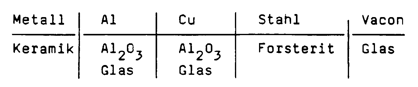
- Als besonders geeignet haben sich die folgenden Werkstoffpaarungen Metallelektrode/Isolierstoffteil herausgestellt:

- Diese Werkstoffe passen im Wellenleiterverhalten gut zueinander, es ergeben sich dabei nahezu verlustlose Wellenleiter. Die Stoffpaarungen Stahl/Forsterit und Vacon/Glas sind außerdem im Temperaturkoeffizienten weitgehend aneinander angepaßt. Die Elektrode und das Isolierstoffteil sind dabei zunächst miteinander mechanisch so verbunden, daß sich eine glatte Wellenleiterfläche ergibt. Vorteilhaft ist weiterhin, wenn das Isolierstoffteil aus einem Material mit relativ kleiner Dielektrizitätskonstante besteht. Dadurch ergibt sich eine günstige Feldverteilung am Ende des vom Plasma erfüllten Teiles des Entladungsraums bei einem in Strahlrichtung des Laserstrahles relativ kurzen Isolierstoffteil.
- Eine einfache, ausreichend kühlbare und plasmastabile Ausführungsform ist gegeben, indem eine Elektrode den gesamten Abstand zwischen den Resonatorspiegeln ausfüllt, indem diese Elektrode elektrisch auf Masse gelegt und mit beiden Spiegeln galvanisch und thermisch leitend verbunden ist, indem nur diese Elektrode Kühlmittelkanäle enthält und indem die gegenüberliegende Elektrode beidseitig über Isolierstoffteile mit den Resonatorspiegeln verbunden ist. Hier wird das Plasma vom Spiegel ferngehalten. Die geerdete Elektrode ermöglicht außerdem einen stabilen Aufbau und vermeidet alle Probleme mit einer spannungsmäßigen Abtrennung der Kühlmittelleitung von der Elektrode.
- Die Erfindung wird nun anhand von drei Figuren näher erläutert. Sie ist nicht auf die in den Figuren gezeigte Beispiele beschränkt.
- FIG 1
- zeigt einen Schnitt eines ersten,
- FIG 2
- zeigt eine Draufsicht und
- FIG 3
- einen Schnitt durch einen zweiten erfindungsgemäßen Bandleiter- oder Slablaser schematisch.
- In einem erfindungsgemäßen Bandleiterlaser liegen sich Elektroden 1 und 2 bezogen auf einen Entladungsspalt 7 gegenüber. An die Elektrode 1 grenzt auf beiden Seiten ein Isolierstoffteil 4 und an dieses je ein Spiegel 5 bzw. 6 an. Die gegenüberliegende Elektrode 2 grenzt unmittelbar an die Spiegel 5 und 6 an. Die Elektrode 1 und die Isolierstoffteile 4 bilden gemeinsam eine Wellenleiterfläche 8. Hierzu sind die Isolierstoffteile 4 mit einer Schicht 10 aus gut wellenleitendem Material beschichtet, wobei die Wellenleitereigenschaften der Schicht 10 an die der Elektrode 1 angepaßt sind. Die Elektrode 1 und die Schicht 10 sind nach dem Zusammenbau der Elektrode 1 mit den Isolierstoffteilen 4 gemeinsam geglättet, beispielsweise geläppt und/oder poliert. Dadurch ergibt sich eine Wellenleiterfläche hoher Güte und ohne Sprünge in den Wellenleitereigenschaften. Dadurch werden die Verluste kleingehalten und eine lokale Überhitzung und Zerstörung der Wellenleiterfläche am Übergang von einem Material zum anderen vermieden. Die Leistungsfähigkeit der beschriebenen Anordnung ist besonders hoch, da einerseits die Spiegel unmittelbar am Wellenleiter anliegen, so daß Streuungen und Verluste durch die Divergenz des Laserlichtes ausgeschaltet sind und da andererseits weder Überschläge von der Elektrode 1 auf die Spiegel 5, 6 noch eine Schädigung der Spiegel durch das Plasma möglich ist. Wird ein Spiegel 5, 6 aus einem plasmaunempfindlichen Isolierstoff hergestellt, beispielsweise aus GaAs oder Si oder Ge, dann kann das entsprechende Isolierstoffteil 4 entfallen und die Elektrode 1 an den Spiegel heranreichen. Diese Stoffe sind teuer. Bei höheren Belastungen empfiehlt es sich generell, einen Aufbau mit Isolierstoffteilen 4, 12, 13 einzusetzen, wie auch in den FIG 2 und 3 gezeigt. In diesem Beispiel ist eine geerdete und gekühlte Elektrode 2 eingesetzt. Die zweite Elektrode 18 ist hier beidseitig mit Isolierstoffteilen 12, 13 gegen die Spiegel 5, 6 abgesetzt. Die Elektrode 18 enthält zumindest einen Kühlkanal 16, an den ein Anschlußrohr 14 anschließt. Auch Wasser ist als Kühlmittel einsetzbar.
- Die Elektrode 2 ist auf Masse gelegt und enthält Kühlkanäle 3, die an zumindest zwei Stellen in Kühlmittelleitungen 15, 17 einmünden. Die von der Elektrode 2 gebildete Wellenleiterfläche 9 geht von Spiegel zu Spiegel durch. So ergibt sich eine gute Kühlung über die gesamte Länge des Entladungsspaltes, die insbesondere bei geringen Spaltdicken des Entladungsspaltes 7 auch für höhere Laserleistungen ausreicht. Die Spiegel 5, 6 sind mit der Elektrode 2 galvanisch leitend verbunden.
- Die Isolierstoffteile 4 bzw. 12, 13 sind so dimensioniert, daß an keiner Stelle ein Überschlag zum Spiegel 5, 6 möglich ist und daß das Plasma im Bereich der Isolierstoffteile 4,12, 13 aufgrund der Feldverteilung vor dem Erreichen des Spiegels 5, 6 endet oder zumindest auf einen unkritisch geringen Wert abfällt. Das Plasma wird im Bereich der Isolierstoffteile 4, 12, 13 zur Elektrode hin entladen, Lichtbögen aus dem Plasma werden auf die Elektrode 2 gezogen, die Spiegel 5, 6 bleiben unversehrt.
- Der Spiegel 5 ist konkav, der Spiegel 6 konvex gewölbt. Die Spiegel bilden einen instabilen Resonator. Ein Fenster 11 stellt den Strahlaustritt dar.
Claims (7)
- Elektrisch angeregter Bandleiterlaser, welcher zwei Wellenleiterflächen (8,9), zwei Resonatorspiegel (5,6) und zumindest zwei Entladungselektroden (1,2) enthält, wobei die Elektroden einander bezogen auf die Strahlrichtung gegenüber liegen und wobei Wellenleiterflächen bis an die Resonatorspiegel heranreichen und aus elektrisch nichtleitenden und metallischen Teilflächen zusammengesetzt sind, dadurch gekennzeichnet, daß eine der Wellenleiterflächen aus einer Elektrode (1) und zumindest einem daran in Strahlrichtung angrenzenden Isolierstoffteil (4) zusammengesetzt ist, daß die zweite Elektrode (2) das Isolierstoffteil in Strahlrichtung überlappt und daß das Isolierstoffteil aus einem Werkstoff mit vorteilhaftem Wellenleitereigenschaften für die Laserstrahlung besteht.
- Bandleiterlaser nach Anspruch 1, dadurch gekennzeichnet, daß an das Isolierstoffteil ein Spiegel aus Metall, insbesondere Kupfer, angrenzt.
- Bandleiterlaser nach Anspruch 1, dadurch gekennzeichnet, daß an das Isolierstoffteil ein Spiegel aus elektrisch isolierendem Material angrenzt.
- Bandleiterlaser nach Anspruch 1, dadurch gekennzeichnet, daß das Material der Elektrode und das des Isolierstoffteiles im Temperaturausdehnungskoeffizienten aufeinander angepaßt sind und daß das Isolierstoffteil auf der dem Entladungskanal zugewandten Seite mit einer Schicht mit vorteilhaften Wellenleitereigenschaften versehen ist.
- Bandleiterlaser nach Anspruch 1, dadurch gekennzeichnet, daß die Werkstoffpaarung für die Elektrode und für das Isolierstoffteil aus der folgenden Tabelle ausgewählt ist:
- Bandleiterlaser nach Anspruch 1, dadurch gekennzeichnet, daß das Isolierstoffteil aus einem Material mit einer relativ kleinen Dielektrizitätskonstante besteht.
- Bandleiterlaser nach einem der Ansprüche 1 bis 6, dadurch gekennzeichnet, daß eine Elektrode den gesamten Abstand zwischen den Resonatorspiegeln ausfüllt, daß diese Elektrode (2) elektrisch auf Masse gelegt und mit beiden Spiegeln galvanisch leitend verbunden ist, daß nur diese Elektrode Kühlmittelkanäle (3) enthält und daß die gegenüberliegende Elektrode beidseitig über Isolierstoffteile mit den Resonatorspiegeln verbunden ist.
Applications Claiming Priority (2)
| Application Number | Priority Date | Filing Date | Title |
|---|---|---|---|
| DE4010147 | 1990-03-29 | ||
| DE4010147A DE4010147A1 (de) | 1990-03-29 | 1990-03-29 | Elektrisch angeregter bandleiterlaser |
Publications (3)
| Publication Number | Publication Date |
|---|---|
| EP0451483A2 EP0451483A2 (de) | 1991-10-16 |
| EP0451483A3 EP0451483A3 (en) | 1991-11-13 |
| EP0451483B1 true EP0451483B1 (de) | 1994-01-19 |
Family
ID=6403350
Family Applications (1)
| Application Number | Title | Priority Date | Filing Date |
|---|---|---|---|
| EP91102975A Expired - Lifetime EP0451483B1 (de) | 1990-03-29 | 1991-02-27 | Elektrisch angeregter Bandleiterlaser |
Country Status (4)
| Country | Link |
|---|---|
| US (1) | US5127017A (de) |
| EP (1) | EP0451483B1 (de) |
| JP (1) | JPH0774415A (de) |
| DE (2) | DE4010147A1 (de) |
Families Citing this family (5)
| Publication number | Priority date | Publication date | Assignee | Title |
|---|---|---|---|---|
| US5231644A (en) * | 1990-09-26 | 1993-07-27 | Siemens Aktiengesellschaft | Slab or stripline gas laser |
| US5216689A (en) * | 1990-10-12 | 1993-06-01 | Coherent, Inc. | Slab laser with enhanced lifetime |
| DE4131623A1 (de) * | 1991-09-23 | 1993-03-25 | Siemens Ag | Bandleiterlaser |
| US7756182B2 (en) * | 2007-03-28 | 2010-07-13 | Coherent, Inc. | RF excited CO2 slab laser tube housing and electrodes cooling |
| US10644474B2 (en) * | 2018-03-07 | 2020-05-05 | Coherent, Inc. | Conductively-cooled slab laser |
Family Cites Families (3)
| Publication number | Priority date | Publication date | Assignee | Title |
|---|---|---|---|---|
| US4908585A (en) * | 1985-04-30 | 1990-03-13 | Chenausky Peter P | RF transformer and diagnostic technique therefor |
| US4890294A (en) * | 1987-01-26 | 1989-12-26 | Mitsubishi Denki Kabushiki Kaisha | Plasma apparatus |
| DE3729053A1 (de) * | 1987-08-31 | 1989-03-16 | Deutsche Forsch Luft Raumfahrt | Hochleistungs-bandleiterlaser |
-
1990
- 1990-03-29 DE DE4010147A patent/DE4010147A1/de not_active Withdrawn
-
1991
- 1991-02-27 US US07/661,220 patent/US5127017A/en not_active Expired - Fee Related
- 1991-02-27 DE DE91102975T patent/DE59100874D1/de not_active Expired - Fee Related
- 1991-02-27 EP EP91102975A patent/EP0451483B1/de not_active Expired - Lifetime
- 1991-03-27 JP JP3089650A patent/JPH0774415A/ja active Pending
Also Published As
| Publication number | Publication date |
|---|---|
| EP0451483A2 (de) | 1991-10-16 |
| DE59100874D1 (de) | 1994-03-03 |
| EP0451483A3 (en) | 1991-11-13 |
| JPH0774415A (ja) | 1995-03-17 |
| DE4010147A1 (de) | 1991-10-02 |
| US5127017A (en) | 1992-06-30 |
Similar Documents
| Publication | Publication Date | Title |
|---|---|---|
| EP0305893B1 (de) | Hochleistungs-Bandleiterlaser | |
| DE19633078C2 (de) | Dielektrischer Wellenleiter | |
| DE3028461C2 (de) | ||
| DE19918567C2 (de) | Verbindungsanordnung für dielektrische Wellenleiter | |
| DE4407251A1 (de) | Nicht strahlender dielektrischer Hohlleiter und Herstellungsverfahren für diesen | |
| DE3215087A1 (de) | Fensteranordnung fuer einen mikrowellenleiter | |
| DE69523699T2 (de) | Einrichtung die einen nicht strahlenden dielektrischen Mikrowellenleiter enthält | |
| DE60307903T2 (de) | Impedanzanpassungskoppler | |
| DE3852981T2 (de) | Matrix aus koaxialen Leitungen mit planaren Überkreuzungen. | |
| EP0886896A1 (de) | Bandleiterlaser | |
| EP0451483B1 (de) | Elektrisch angeregter Bandleiterlaser | |
| DE2752333A1 (de) | Streifenleitungs-kondensator | |
| DE2506425C2 (de) | Hohlleiter/Microstrip-Übergang | |
| DE102012222469B4 (de) | Diffusionsgekühlte Gaslaseranordnung und Verfahren zur Einstellung der Entladungsverteilung bei einer diffusionsgekühlten Gaslaseranordnung | |
| DE3446196C1 (de) | Hohlleiterbauelement mit stark verlustbehaftetem Werkstoff | |
| EP0403907A1 (de) | Auskopplungsfenster für linear polarisierte Mikrowellen | |
| EP0392485A1 (de) | Gaslaser mit Mikrowellenanregung | |
| EP2553757B1 (de) | Koaxialleiterstruktur | |
| EP0477879A1 (de) | Für hohe Eingangsleistung geeigneter elektrisch gepumpter Gaslaser | |
| DE2525845B2 (de) | Breitbandig reflexionsarm bedaempfte verzoegerungsleitung und verfahren zu ihrer herstellung | |
| DE69934968T2 (de) | Breitbandiger übergang von mikrostreifenleitung auf parallelplatten-hohlleiter | |
| EP0276443B1 (de) | Quer angeregter Wellenleiter-Laser | |
| EP0594672B1 (de) | Gaslaser, insbesondere co2-laser | |
| EP4080999B1 (de) | Hochfrequenz-zuleitung und elektronische komponente mit hochfrequenz-zuleitung | |
| DE4205577A1 (de) | Breitbandige hohlleiter-serien-parallelverzweigung |
Legal Events
| Date | Code | Title | Description |
|---|---|---|---|
| PUAI | Public reference made under article 153(3) epc to a published international application that has entered the european phase |
Free format text: ORIGINAL CODE: 0009012 |
|
| PUAL | Search report despatched |
Free format text: ORIGINAL CODE: 0009013 |
|
| AK | Designated contracting states |
Kind code of ref document: A2 Designated state(s): DE FR GB IT |
|
| AK | Designated contracting states |
Kind code of ref document: A3 Designated state(s): DE FR GB IT |
|
| 17P | Request for examination filed |
Effective date: 19920110 |
|
| 17Q | First examination report despatched |
Effective date: 19930302 |
|
| GRAA | (expected) grant |
Free format text: ORIGINAL CODE: 0009210 |
|
| AK | Designated contracting states |
Kind code of ref document: B1 Designated state(s): DE FR GB IT |
|
| REF | Corresponds to: |
Ref document number: 59100874 Country of ref document: DE Date of ref document: 19940303 |
|
| ITF | It: translation for a ep patent filed | ||
| GBT | Gb: translation of ep patent filed (gb section 77(6)(a)/1977) |
Effective date: 19940325 |
|
| ET | Fr: translation filed | ||
| PLBE | No opposition filed within time limit |
Free format text: ORIGINAL CODE: 0009261 |
|
| STAA | Information on the status of an ep patent application or granted ep patent |
Free format text: STATUS: NO OPPOSITION FILED WITHIN TIME LIMIT |
|
| 26N | No opposition filed | ||
| PGFP | Annual fee paid to national office [announced via postgrant information from national office to epo] |
Ref country code: FR Payment date: 19950227 Year of fee payment: 5 |
|
| PG25 | Lapsed in a contracting state [announced via postgrant information from national office to epo] |
Ref country code: FR Effective date: 19961031 |
|
| REG | Reference to a national code |
Ref country code: FR Ref legal event code: ST |
|
| REG | Reference to a national code |
Ref country code: GB Ref legal event code: 732E |
|
| REG | Reference to a national code |
Ref country code: GB Ref legal event code: 732E |
|
| PGFP | Annual fee paid to national office [announced via postgrant information from national office to epo] |
Ref country code: GB Payment date: 19990304 Year of fee payment: 9 |
|
| PGFP | Annual fee paid to national office [announced via postgrant information from national office to epo] |
Ref country code: DE Payment date: 19990306 Year of fee payment: 9 |
|
| PG25 | Lapsed in a contracting state [announced via postgrant information from national office to epo] |
Ref country code: GB Free format text: LAPSE BECAUSE OF NON-PAYMENT OF DUE FEES Effective date: 20000227 |
|
| GBPC | Gb: european patent ceased through non-payment of renewal fee |
Effective date: 20000227 |
|
| PG25 | Lapsed in a contracting state [announced via postgrant information from national office to epo] |
Ref country code: DE Free format text: LAPSE BECAUSE OF NON-PAYMENT OF DUE FEES Effective date: 20001201 |
|
| PG25 | Lapsed in a contracting state [announced via postgrant information from national office to epo] |
Ref country code: IT Free format text: LAPSE BECAUSE OF NON-PAYMENT OF DUE FEES;WARNING: LAPSES OF ITALIAN PATENTS WITH EFFECTIVE DATE BEFORE 2007 MAY HAVE OCCURRED AT ANY TIME BEFORE 2007. THE CORRECT EFFECTIVE DATE MAY BE DIFFERENT FROM THE ONE RECORDED. Effective date: 20050227 |