EP0451646A2 - Dispositif de circuit de correction d'erreur double et de détection d'erreur triple - Google Patents
Dispositif de circuit de correction d'erreur double et de détection d'erreur triple Download PDFInfo
- Publication number
- EP0451646A2 EP0451646A2 EP91105044A EP91105044A EP0451646A2 EP 0451646 A2 EP0451646 A2 EP 0451646A2 EP 91105044 A EP91105044 A EP 91105044A EP 91105044 A EP91105044 A EP 91105044A EP 0451646 A2 EP0451646 A2 EP 0451646A2
- Authority
- EP
- European Patent Office
- Prior art keywords
- data stream
- errors
- reading
- string
- generating
- Prior art date
- Legal status (The legal status is an assumption and is not a legal conclusion. Google has not performed a legal analysis and makes no representation as to the accuracy of the status listed.)
- Withdrawn
Links
Images
Classifications
-
- G—PHYSICS
- G06—COMPUTING OR CALCULATING; COUNTING
- G06F—ELECTRIC DIGITAL DATA PROCESSING
- G06F11/00—Error detection; Error correction; Monitoring
- G06F11/22—Detection or location of defective computer hardware by testing during standby operation or during idle time, e.g. start-up testing
- G06F11/2205—Detection or location of defective computer hardware by testing during standby operation or during idle time, e.g. start-up testing using arrangements specific to the hardware being tested
- G06F11/2215—Detection or location of defective computer hardware by testing during standby operation or during idle time, e.g. start-up testing using arrangements specific to the hardware being tested to test error correction or detection circuits
-
- H—ELECTRICITY
- H03—ELECTRONIC CIRCUITRY
- H03M—CODING; DECODING; CODE CONVERSION IN GENERAL
- H03M13/00—Coding, decoding or code conversion, for error detection or error correction; Coding theory basic assumptions; Coding bounds; Error probability evaluation methods; Channel models; Simulation or testing of codes
- H03M13/03—Error detection or forward error correction by redundancy in data representation, i.e. code words containing more digits than the source words
- H03M13/05—Error detection or forward error correction by redundancy in data representation, i.e. code words containing more digits than the source words using block codes, i.e. a predetermined number of check bits joined to a predetermined number of information bits
- H03M13/13—Linear codes
- H03M13/15—Cyclic codes, i.e. cyclic shifts of codewords produce other codewords, e.g. codes defined by a generator polynomial, Bose-Chaudhuri-Hocquenghem [BCH] codes
Definitions
- the present invention is concerned with a circuit device for correction of double errors and detection of triple errors.
- the main object of the present invention is to solve the aforementioned problem and therefore to eliminate the abovementioned drawbacks by realizing a circuit device for correction of double errors and detection of triple errors which is able to perform coding, error correction and detection functions with a considerable reduction in power consumption, according an integrable structure, thus providing a higher reliability while avoiding the use of burdensome external memories for decoding.
- the basic idea of the invention is to provide a transmitting block having two separate coding sections connected in series, one for double-error correction and one for triple error detection, and a receiving block having two corresponding decoding sections, and testing means for testing the working of the circuit device. Both, coding and decoding sections work in an algorithmic way.
- BCH means Binary Code Hamming, which is the decoding form according to Hamming binary logic theory to which reference has to be made for details.
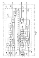
- 1 stands for the circuit device whereon are a transmission block 2 and a receive block 3.
- transmission block 2 Within transmission block 2 is a timing circuitry 4 for generating the control signals for all the circuit sections present in block 2, and a circuitry 5 for generating desired errors at the output of a section 9, which is a multiplexer.
- Numeral reference 6 indicates a coding circuitry according BCH (127, 113) code, which allows the coding of a serial data stream in one hundred thirteen bits received at an input or pin 6a.
- BCH 127, 113 code
- Numeral reference 7 indicates a circuitry which allows a parity generation
- 8 stands for another circuitry for coding the parity check signal from section 7.
- Signal 4a starts the operation of the relative timing section 4 so as to allow the coding of the serial data stream transmitted via the input 6a.
- Exclusive OR 10 By means of an Exclusive OR 10 it is possible to invert the output bits in order to provide an output 10a according to what expected, with desired number and position of error bits.
- Reference 9a indicates the normal output, i.e., the corresponding output of the transmission block 2.
- the output 10a goes to section 13 through a multiplexer 11.
- At the input of multiplexer 11 is also input 11b, which is the normal input of the receive block 3.
- Through a select signal 11a it is possible to decide which of the two signals 10a und 11b send to section 13.
- the signal is then transmitted to a section 13 which substantially calculates the syndrome on the first, more significant, one hundred twenty seven bits received and at whose output power sums 13a and 13b, which result from the processing of the received data stream, are generated.
- timing section 12 similar to section 4 of receive block 2.
- timing section 12 receives in turn a start pin 12a which activates the relative circuitry.
- a double-error detection section 14 By means of a double-error detection section 14 the eventual errors present in the received code are detected and thus sent, through relative addressing by the signals 14a and 14b, to another section 15 which is a double-error correction section.
- Such section generates a correction signal 15a in a proper position for a maximum of two errors present in the data code.
- section 17 it is possible to delay data entering block 3 and such section 17 presents at the output a signal 17a which will enter one of the inputs of an Exclusive OR 18 and will then add to the correction signal 15a from section 15.
- the output from section 18 will enter an input of a last section 16, representing a circuitry which detects the presence of triple errors.
- Such triple-error detection section 16 will then generate an error signal 16a at the output, if any coding irregularity in the data stream has been detected.
- the normal output receive block 3 is signal 18a.
- the circuit device is designated as FEC (Forward Error Correction) i.e., error correction in successive steps.
- FEC Forward Error Correction
- the device makes use of error correction code of BCH (127, 113) type.
- This code has an Hamming distance equal to 5, i.e., the difference between any two codes is not less than 5 bis, therefore is able to correct all single and double errors on the group of the one hundred twenty seven bits; for this purpose a field of 14 bits is added to the 113 bits.
- the BCH (127, 113) block and the global parity bit are decoded separately by using the two coding sections indicated in figure by 6 and 8, as well as by parity generator 7.
- a first coding is realized on the block of one hundred thirteen symbols (i.e. bits) which are to be transmitted according to a polynomial generating the BCH (127, 113) code which, from an algebraic viewpoint, may be represented as: 1 + x + x2 + x4 + x5 + x6 + x8 + x9 + x14.
- a parity field is added calculated on the one hundred seven eight bits and coded according to code (5, 1).
- a block code (132, 113) is so obtained and then transmitted.
- the start signal is given through the input 4 which serves for activating all the circuitry.
- the 132 bits are sent to section 13, but only the 113 original bits are sent to section 17 for delaying and synchronization purpose.
- the 113 corrected bits outputted form section 18 are sent to section 16 where first are codified into 127 bits, second a parity bit is computed on such 127 bits, third the computed 14 bits are extracted from such 127 bits and last a second redundancy, comprising the parity bit and the 14 bits, is obtained.
- the two redundancies are compared in section 16 and, if different, the presence of three errors, obviously not corrected, is detected in the received one hundred twenty seven bits. Then an error signal 16a will be present at the output of section 16 which can be read and detected.
- section 6 of transmission block 2 the coding of a serial data stream in one hundred thirteen bits received at its input, represented by pin 6a, is performed.
- Coding is performed by generating 14 bits, called as above redundancy bits to be added to the already existent one hundred thirteen bits so as to form a data stream or block of one hundred twenty seven bits coded according to BCH (127, 113) cyclic Hamming code.
- a parity check on said one hundred twenty seven bits is then carried out by section 7, generating a bit equal to 1 if the number of ones therein contained is odd, or equal to 0 if such number is even.
- Such coding may be set up externally so as to obtain a block code (5, 1), a data stream is thus generated which will be added in the multiplexer 9, to the end in the data stream of one hundred twenty seven bits form coder 6, thus providing a serial data stream of one hundred thirty two bitds at the output pin 9a.
- the timer 4, as well as the one 12 of receive block 3, generates all the control signals for the management of the various circuitries present in block 2 and 3. Moreover, it is possible to choose the type of parity control through input pin 4b.
- Section 5 is an error generator which under circuit test conditions generates an error data stream 5b to be added to the data flow outgoing from the multiplexer section 9.
- control signals from a generic external microprocessor connected to device 1 via the input 5a, on which two address lines are also connected.
- the external microprocessor through writing on special internal registers not shwon in figure, can program the location of three errors at most in the 132 bits.
- the external microprocessor has the chance to check wether the 113 bits sent to the transmitting block 2 and the 113 bits outputted by the receive block 3 are identical. Using different numbers and positions of errors the microprocessor can make a test of the circuit device during both operation and non-operation conditions.
- the two inputs inside block 14 allow the calculation of eventual errors present in the received code, the eventual detection of position and then the transmission of the relative result to correction block 15.
- Block 17 which is a data buffer, i.e., a data memory, is used for delaying input data in receive block 3 so taht this will be in phase coincidence with correction signal 15a.
- a signal 17a will be present at the output and will enter the exclusive OR 18, and at the other input of the same exclusive OR 18 is a correction signal 15a which will perform error correction by adding itself to 17a.
- block 16 it is possible to detect the presence of three errors in the data code; in such event no correction occurs but an error signal 16a is present at the output of device 1 and indicates thus a useful information to the external microprocessor for an eventual retransmission of the previously transmitted data stream.
- the error correction is a FEC type correction.
Landscapes
- Engineering & Computer Science (AREA)
- Physics & Mathematics (AREA)
- Theoretical Computer Science (AREA)
- General Engineering & Computer Science (AREA)
- General Physics & Mathematics (AREA)
- Computer Hardware Design (AREA)
- Probability & Statistics with Applications (AREA)
- Pure & Applied Mathematics (AREA)
- Mathematical Physics (AREA)
- Algebra (AREA)
- Quality & Reliability (AREA)
- Detection And Correction Of Errors (AREA)
- Radar Systems Or Details Thereof (AREA)
- Optical Radar Systems And Details Thereof (AREA)
- Detection And Prevention Of Errors In Transmission (AREA)
- Error Detection And Correction (AREA)
Applications Claiming Priority (2)
| Application Number | Priority Date | Filing Date | Title |
|---|---|---|---|
| IT19958A IT1239530B (it) | 1990-04-06 | 1990-04-06 | Dispositivo circuitale per la correzione di errori doppi e la rilevazione di errori tripli |
| IT1995890 | 1990-04-06 |
Publications (2)
| Publication Number | Publication Date |
|---|---|
| EP0451646A2 true EP0451646A2 (fr) | 1991-10-16 |
| EP0451646A3 EP0451646A3 (en) | 1993-03-17 |
Family
ID=11162648
Family Applications (1)
| Application Number | Title | Priority Date | Filing Date |
|---|---|---|---|
| EP19910105044 Withdrawn EP0451646A3 (en) | 1990-04-06 | 1991-03-28 | Circuit device for correction of double errors and detection of triple errors |
Country Status (2)
| Country | Link |
|---|---|
| EP (1) | EP0451646A3 (fr) |
| IT (1) | IT1239530B (fr) |
Family Cites Families (2)
| Publication number | Priority date | Publication date | Assignee | Title |
|---|---|---|---|---|
| US4117458A (en) * | 1977-03-04 | 1978-09-26 | Grumman Aerospace Corporation | High speed double error correction plus triple error detection system |
| US4736376A (en) * | 1985-10-25 | 1988-04-05 | Sequoia Systems, Inc. | Self-checking error correcting encoder/decoder |
-
1990
- 1990-04-06 IT IT19958A patent/IT1239530B/it active IP Right Grant
-
1991
- 1991-03-28 EP EP19910105044 patent/EP0451646A3/en not_active Withdrawn
Also Published As
| Publication number | Publication date |
|---|---|
| IT9019958A1 (it) | 1991-10-06 |
| IT1239530B (it) | 1993-11-05 |
| EP0451646A3 (en) | 1993-03-17 |
| IT9019958A0 (it) | 1990-04-06 |
Similar Documents
| Publication | Publication Date | Title |
|---|---|---|
| EP1160987B1 (fr) | Méthode et dispositif de vérification de codes correcteurs d'erreurs | |
| JP3234130B2 (ja) | 誤り訂正符号復号化方法およびこの方法を用いる回路 | |
| US5384788A (en) | Apparatus and method for optimal error correcting code to parity conversion | |
| US5598424A (en) | Error detection structure and method for serial or parallel data stream using partial polynomial check | |
| JP3325914B2 (ja) | データ用誤り訂正検出方法及びコンピュータ・メモリ用 誤り検出回路 | |
| JPH0812612B2 (ja) | 誤り訂正方法及び装置 | |
| JP3272903B2 (ja) | 誤り訂正検出回路と半導体記憶装置 | |
| US6742159B2 (en) | Address parity error processing method, and apparatus and storage for the method | |
| JPH06324951A (ja) | 誤り検査/訂正機能を有するコンピュータ・システム | |
| EP0037705A1 (fr) | Système de mémoire à correction d'erreurs | |
| GB2226168A (en) | Testing error checking and correction circuit in digital memory device | |
| JPS6346615B2 (fr) | ||
| US5751745A (en) | Memory implemented error detection and correction code with address parity bits | |
| EP0147336A2 (fr) | Système de correction et de détection d'erreurs | |
| EP0753942A2 (fr) | Traitement par mot pour des codes Reed-Solomon | |
| US5761221A (en) | Memory implemented error detection and correction code using memory modules | |
| US6393597B1 (en) | Mechanism for decoding linearly-shifted codes to facilitate correction of bit errors due to component failures | |
| US4404673A (en) | Error correcting network | |
| CN102545914B (zh) | Bch编译码方法及装置 | |
| US3891969A (en) | Syndrome logic checker for an error correcting code decoder | |
| US4384353A (en) | Method and means for internal error check in a digital memory | |
| US20250038769A1 (en) | Syndrome decoder circuit | |
| JPH05216698A (ja) | 改良されたエラー検出および訂正回路 | |
| JPH08293802A (ja) | インターリーブ式誤り訂正方法 | |
| EP1192544B1 (fr) | Circuit et procede de correction d'erreurs destines a un dispositif de memoire |
Legal Events
| Date | Code | Title | Description |
|---|---|---|---|
| PUAI | Public reference made under article 153(3) epc to a published international application that has entered the european phase |
Free format text: ORIGINAL CODE: 0009012 |
|
| AK | Designated contracting states |
Kind code of ref document: A2 Designated state(s): AT BE CH DE ES FR GB IT LI NL SE |
|
| RAP1 | Party data changed (applicant data changed or rights of an application transferred) |
Owner name: ALCATEL FACE S.P.A. |
|
| RAP1 | Party data changed (applicant data changed or rights of an application transferred) |
Owner name: ALCATEL ITALIA S.P.A. |
|
| PUAL | Search report despatched |
Free format text: ORIGINAL CODE: 0009013 |
|
| AK | Designated contracting states |
Kind code of ref document: A3 Designated state(s): AT BE CH DE ES FR GB IT LI NL SE |
|
| 17P | Request for examination filed |
Effective date: 19930716 |
|
| 17Q | First examination report despatched |
Effective date: 19960125 |
|
| STAA | Information on the status of an ep patent application or granted ep patent |
Free format text: STATUS: THE APPLICATION IS DEEMED TO BE WITHDRAWN |
|
| 18D | Application deemed to be withdrawn |
Effective date: 19961203 |