EP0451855A1 - Verfahren zur Herstellung eines epitaktischen Wafers - Google Patents
Verfahren zur Herstellung eines epitaktischen Wafers Download PDFInfo
- Publication number
- EP0451855A1 EP0451855A1 EP91105832A EP91105832A EP0451855A1 EP 0451855 A1 EP0451855 A1 EP 0451855A1 EP 91105832 A EP91105832 A EP 91105832A EP 91105832 A EP91105832 A EP 91105832A EP 0451855 A1 EP0451855 A1 EP 0451855A1
- Authority
- EP
- European Patent Office
- Prior art keywords
- wafer
- epitaxial growth
- vapor
- principal surface
- silicon
- Prior art date
- Legal status (The legal status is an assumption and is not a legal conclusion. Google has not performed a legal analysis and makes no representation as to the accuracy of the status listed.)
- Withdrawn
Links
Images

Classifications
-
- H—ELECTRICITY
- H10—SEMICONDUCTOR DEVICES; ELECTRIC SOLID-STATE DEVICES NOT OTHERWISE PROVIDED FOR
- H10P—GENERIC PROCESSES OR APPARATUS FOR THE MANUFACTURE OR TREATMENT OF DEVICES COVERED BY CLASS H10
- H10P52/00—Grinding, lapping or polishing of wafers, substrates or parts of devices
- H10P52/40—Chemomechanical polishing [CMP]
- H10P52/402—Chemomechanical polishing [CMP] of semiconductor materials
-
- H—ELECTRICITY
- H10—SEMICONDUCTOR DEVICES; ELECTRIC SOLID-STATE DEVICES NOT OTHERWISE PROVIDED FOR
- H10P—GENERIC PROCESSES OR APPARATUS FOR THE MANUFACTURE OR TREATMENT OF DEVICES COVERED BY CLASS H10
- H10P14/00—Formation of materials, e.g. in the shape of layers or pillars
- H10P14/20—Formation of materials, e.g. in the shape of layers or pillars of semiconductor materials
- H10P14/24—Formation of materials, e.g. in the shape of layers or pillars of semiconductor materials using chemical vapour deposition [CVD]
-
- H—ELECTRICITY
- H10—SEMICONDUCTOR DEVICES; ELECTRIC SOLID-STATE DEVICES NOT OTHERWISE PROVIDED FOR
- H10P—GENERIC PROCESSES OR APPARATUS FOR THE MANUFACTURE OR TREATMENT OF DEVICES COVERED BY CLASS H10
- H10P14/00—Formation of materials, e.g. in the shape of layers or pillars
- H10P14/20—Formation of materials, e.g. in the shape of layers or pillars of semiconductor materials
- H10P14/29—Formation of materials, e.g. in the shape of layers or pillars of semiconductor materials characterised by the substrates
- H10P14/2901—Materials
- H10P14/2902—Materials being Group IVA materials
- H10P14/2905—Silicon, silicon germanium or germanium
-
- H—ELECTRICITY
- H10—SEMICONDUCTOR DEVICES; ELECTRIC SOLID-STATE DEVICES NOT OTHERWISE PROVIDED FOR
- H10P—GENERIC PROCESSES OR APPARATUS FOR THE MANUFACTURE OR TREATMENT OF DEVICES COVERED BY CLASS H10
- H10P14/00—Formation of materials, e.g. in the shape of layers or pillars
- H10P14/20—Formation of materials, e.g. in the shape of layers or pillars of semiconductor materials
- H10P14/34—Deposited materials, e.g. layers
- H10P14/3402—Deposited materials, e.g. layers characterised by the chemical composition
- H10P14/3404—Deposited materials, e.g. layers characterised by the chemical composition being Group IVA materials
- H10P14/3411—Silicon, silicon germanium or germanium
-
- H—ELECTRICITY
- H10—SEMICONDUCTOR DEVICES; ELECTRIC SOLID-STATE DEVICES NOT OTHERWISE PROVIDED FOR
- H10P—GENERIC PROCESSES OR APPARATUS FOR THE MANUFACTURE OR TREATMENT OF DEVICES COVERED BY CLASS H10
- H10P50/00—Etching of wafers, substrates or parts of devices
- H10P50/60—Wet etching
- H10P50/64—Wet etching of semiconductor materials
- H10P50/642—Chemical etching
Definitions
- This invention relates to a method of manufacturing an epitaxial wafer, and more particularly to an epitaxial wafer manufacturing method most suitable for highly integrated devices such as 1M, 4M, or 16M bit devices, etc.
- a semiconductor device is formed on a wafer provided by slicing a silicon single crystal obtained by a pulling method.
- the following method is a known method relatively frequently used. Namely, an external shape processing is implemented to a CZ crystal formed by pulling using the Czochralski method so that it is in the form of an accurate cylinder, and is then sliced. Thereafter, etching is implemented in order to remove a damaged layer formed on the surface by machining at the time of slicing. Further, an abrasive process for improvement of flatness or planarization, removal of surface defects, and improvement of surface roughness is implemented.
- micro-defects are given to the crystal by implementing mechanical abrasion to the back surface of the wafer, or spraying, at a high pressure, silicon oxide powder or diffusion liquid into water, to thus form gettering nuclei for capturing polluted atoms.
- This method is certainly effective, but the mechanically processed layer results in a cause of dust. Accordingly, from a microscopic point of view, dust may be produced on the principal surface of the wafer. In this sense, this method is not necessarily satisfactory.
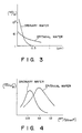
- FIG. 3 is a graph showing, in a comparative manner, what sizes of dust are observed in the case of an ordinary wafer having a diameter of 150 mm and in the case where an epitaxial layer is formed on the ordinary wafer.
- FIG. 4 The comparison between the flatness of the conventional wafer and that of the epitaxial wafer is shown in FIG. 4.
- This figure shows the distribution of an uneveness difference in the cell with 20 mm ⁇ as a unit.
- the peak value of the unevenness difference is deteriorated by 0.2 to 0.5 ⁇ m.
- Such a deterioration is considered to be caused by unevenness of the thickness of the film grown at the time of vapor phase growth, and partial growth of silicon due to flowing to the back surface of the wafer of reaction gas.
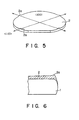
- FIG. 6 is a partial cross sectional view taken along the ⁇ 100 ⁇ direction of the wafer.
- the shape of the crown is shown. It is seen from this figure that the upper end portion of the epitaxial growth layer 2 formed on the beveling processed wafer 1 is extraordinarily grown, resulting in the projection 2a.
- Such a crown not only damages flatness of the wafer, but also causes cracking due to impact of the mechanical processing at the time of handling or occurrence of silicon dust.
- the device function and/or yield may be lowered.
- the yield loss amounts to 20%.
- the yield loss as a material for improving the flatness of a material so that it is equal to 0.5 to 0.7 ⁇ m/20 mm ⁇ will reach 30 to 50 %.
- the distortion formed at a high temperature ranging from 1150 to 1250°C at this process are annealed, or the density is reduced by growth of the epitaxial layer on the back surface of the wafer, resulting in a considerably lowered gettering effect.
- an object of this invention is to provide a method of manufacturing an epitaxial wafer for high integration devices having fewer surface defects and excellent planarization characteristics.
- a method of manufacturing an epitaxial wafer comprises the steps of slicing a silicon single crystal pulled up to provide a wafer, etching the principal surface of the wafer to remove a damaged layer due to slicing of the surface, implementing specular processing to the principal surface, allowing silicon to be subjected to vapor-phase epitaxial growth on the specularly processed principal surface, and implementing specular processing to the principal surface for a second time to remove various defects produced at the time of the vapor phase epitaxial growth to improve flatness.
- a method of manufacturing an epitaxial wafer comprises the steps of slicing a silicon single crystal pulled up to provide a wafer, etching the principal surface of the wafer to remove a damaged layer due to slicing of the surface, allowing silicon to be subjected to vapor-phase epitaxial growth on the etched principal surface, and implementing specular processing to the principal surface on which the vapor-phase epitaxial growth is carried out to remove various defects produced at the time of the vapor-phase epitaxial growth to improve flatness.
- a beveling processing step for removing an extraordinary growth layer produced at the time of the silicon epitaxial growth at the peripheral edge portion of the wafer, and a step for forming backside damage of the wafer.
- FIG. 1 is a flowchart showing a first embodiment of a method of manufacturing an epitaxial wafer according to this invention.
- a silicon single crystal to which external shape processing is implemented is sliced (step S101).
- the silicon single crystal thus sliced is chemically etched to remove a damaged layer produced at the time of slicing (step S102).
- specular processing is implemented to the surface by chemical abrasion (step S103). The planarization of the surface is considerably improved by this specular processing.
- a silicon layer is then formed by epitaxial growth (step S104).
- a wafer is heated at about 1150°C in the atmosphere of hydrogen to introduce a mixture of silicon compound and carrier gas to form decomposed silicon atoms as a single crystal layer 10 to 20 ⁇ m thick on a silicon substrate.
- a silicon compound silicon tetrachloride (SiH4), trichlorosilane (SiHCl3), or dichlorosilane (SiH2Cl2), etc. may be used.
- specular processing by chemical abrasive process is carried out for a second time (step S105).
- This second specular processing is carried out in order to remove dust and crown causing deterioration of flatness, which are produced in the epitaxial growth, and attached dust.
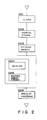
- FIG. 2 is a flowchart showing a second embodiment of a method of manufacturing an epitaxial wafer according to this invention.
- a silicon single crystal to which external processing is implemented is sliced (step S201).
- the silicon single crystal thus sliced is chemically etched to remove a damaged layer produced at the time of slicing.
- a silicon layer is then formed by vapor-phase epitaxial growth on the etched surface (step S203).
- the epitaxial growth condition is the same as that in the case of FIG. 1.
- Beveling processing for removing the peripheral edge portion of the upper surface of the wafer is then carried out (step S204).
- growth of the ⁇ 100 ⁇ orientation is fast at the time of vapor-phase growth of silicon, so crown is apt to take place on the (110) plane.
- the above-mentioned beveling processing is implemented in order to remove such a crown.
- Honing processing for forming processed distortions having gettering effect is implemented to the back surface of the wafer after vapor-phase epitaxial growth (step S205). While this processed distortion formation process may be added also before the vapor-phase epitaxial growth process, since distortion may be reduced at the vapor-phase epitaxial growth process as previously described, it is desirable to newly add such processed distortion formation process. Steps S204 and S205 are addition processes for improving the characteristic of the wafer.
- specular processing by chemical abrasion is carried out for a second time (step S206). This specular processing is carried out in order to remove defects produced at the epitaxial growth process step and process steps succeeding thereto to improve flatness.
- the boundary between the silicon base layer and the epitaxial growth layer has a degree of unevenness greater than that of the specular surface of the wafer surface from a microscopic point of view.
- the adverse influence on the electric characteristic was not particularly observed in devices using only a surface area as an active area as in MOS device.
- the beveling processing and the honing processing may be carried out in reverse order. Further, without carrying out these processing, the method of this invention may be implemented so as to immediately shift from the vapor-phase epitaxial growth process step to the specular processing step.
Applications Claiming Priority (2)
| Application Number | Priority Date | Filing Date | Title |
|---|---|---|---|
| JP2097219A JPH0817163B2 (ja) | 1990-04-12 | 1990-04-12 | エピタキシャルウェーハの製造方法 |
| JP97219/90 | 1990-04-12 |
Publications (1)
| Publication Number | Publication Date |
|---|---|
| EP0451855A1 true EP0451855A1 (de) | 1991-10-16 |
Family
ID=14186522
Family Applications (1)
| Application Number | Title | Priority Date | Filing Date |
|---|---|---|---|
| EP91105832A Withdrawn EP0451855A1 (de) | 1990-04-12 | 1991-04-12 | Verfahren zur Herstellung eines epitaktischen Wafers |
Country Status (3)
| Country | Link |
|---|---|
| EP (1) | EP0451855A1 (de) |
| JP (1) | JPH0817163B2 (de) |
| KR (1) | KR920005807A (de) |
Cited By (8)
| Publication number | Priority date | Publication date | Assignee | Title |
|---|---|---|---|---|
| EP0617456A3 (de) * | 1993-03-08 | 1995-12-27 | Gi Corp | Billiges Verfahren zur Herstellung von epitaktischen Halbleiteranordnungen. |
| US6365461B1 (en) * | 1999-10-07 | 2002-04-02 | Sumitomo Metal Industries, Ltd. | Method of manufacturing epitaxial wafer |
| EP0989600A3 (de) * | 1998-09-25 | 2003-09-10 | Sumitomo Electric Industries, Ltd. | Oberflächenreinigungsverfahren zur Herstellung von epitaktischen II-VI Verbindungshalbleiterscheiben |
| EP1988193A4 (de) * | 2006-01-31 | 2009-07-22 | Sumco Corp | Herstellungsverfahren für einen epitaktischen wafer |
| TWI418648B (zh) * | 2007-06-26 | 2013-12-11 | Sumco Corp | Epitaxial wafer and its manufacturing method |
| US9340900B2 (en) * | 2006-09-06 | 2016-05-17 | Sumco Corporation | Epitaxial wafer and method of producing same |
| CN106068546A (zh) * | 2014-03-05 | 2016-11-02 | 信越半导体株式会社 | 半导体外延晶圆的制造方法及半导体外延晶圆 |
| CN107004583A (zh) * | 2014-12-02 | 2017-08-01 | 昭和电工株式会社 | 晶片支承台、化学气相生长装置、外延晶片及其制造方法 |
Families Citing this family (10)
| Publication number | Priority date | Publication date | Assignee | Title |
|---|---|---|---|---|
| JP2639744B2 (ja) * | 1990-07-09 | 1997-08-13 | 三菱マテリアル株式会社 | シリコンウェーハおよびその製造方法 |
| US6458205B1 (en) * | 1999-04-20 | 2002-10-01 | Shin-Etsu Handotai Co., Ltd. | Silicon epitaxial wafer and its manufacturing method |
| JP4528599B2 (ja) * | 2004-10-25 | 2010-08-18 | Sumco Techxiv株式会社 | エピタキシャル基板の製造方法 |
| TWI370184B (en) * | 2006-09-06 | 2012-08-11 | Sumco Corp | Epitaxial wafer and method of producing same |
| JP4935572B2 (ja) * | 2007-08-09 | 2012-05-23 | 信越半導体株式会社 | 高輝度発光ダイオードの製造方法 |
| JP5212472B2 (ja) * | 2008-06-10 | 2013-06-19 | 株式会社Sumco | シリコンエピタキシャルウェーハの製造方法 |
| JP5287982B2 (ja) | 2009-04-13 | 2013-09-11 | 株式会社Sumco | シリコンエピタキシャルウェーハの製造方法 |
| JP5795461B2 (ja) | 2009-08-19 | 2015-10-14 | 株式会社Sumco | エピタキシャルシリコンウェーハの製造方法 |
| JP5757088B2 (ja) * | 2011-01-05 | 2015-07-29 | 株式会社Sumco | エピタキシャルウェーハの製造方法、エピタキシャルウェーハ |
| JP6015127B2 (ja) * | 2012-05-23 | 2016-10-26 | 株式会社デンソー | 半導体装置の製造方法およびそれに用いられる半導体基板 |
Citations (3)
| Publication number | Priority date | Publication date | Assignee | Title |
|---|---|---|---|---|
| GB2014790A (en) * | 1978-02-20 | 1979-08-30 | Hitachi Ltd | Semiconductor substrate and method of manufacture thereof |
| EP0319805A1 (de) * | 1987-11-28 | 1989-06-14 | Kabushiki Kaisha Toshiba | Verfahren zur Behandlung eines Plättchens |
| US4885056A (en) * | 1988-09-02 | 1989-12-05 | Motorola Inc. | Method of reducing defects on semiconductor wafers |
Family Cites Families (7)
| Publication number | Priority date | Publication date | Assignee | Title |
|---|---|---|---|---|
| JPS5534454A (en) * | 1978-08-31 | 1980-03-11 | Nec Corp | Preparation of semiconductor substrate with epitaxial layer |
| JPS5844725A (ja) * | 1981-09-11 | 1983-03-15 | Komatsu Denshi Kinzoku Kk | 半導体シリコン基板の製造方法 |
| JPS592317A (ja) * | 1982-06-28 | 1984-01-07 | Nec Corp | 半導体装置の製造方法 |
| JPS60198811A (ja) * | 1984-03-23 | 1985-10-08 | Mitsubishi Electric Corp | 半導体装置の製造方法 |
| JPS60246637A (ja) * | 1984-05-21 | 1985-12-06 | Mitsubishi Electric Corp | 半導体装置の製造方法 |
| JPH0646622B2 (ja) * | 1987-06-30 | 1994-06-15 | 三菱電機株式会社 | 半導体基板用シリコンウェハの製造方法 |
| JPH01201922A (ja) * | 1988-02-05 | 1989-08-14 | Nec Corp | ウェハーの製造方法 |
-
1990
- 1990-04-12 JP JP2097219A patent/JPH0817163B2/ja not_active Expired - Lifetime
-
1991
- 1991-04-11 KR KR1019910005752A patent/KR920005807A/ko not_active Abandoned
- 1991-04-12 EP EP91105832A patent/EP0451855A1/de not_active Withdrawn
Patent Citations (3)
| Publication number | Priority date | Publication date | Assignee | Title |
|---|---|---|---|---|
| GB2014790A (en) * | 1978-02-20 | 1979-08-30 | Hitachi Ltd | Semiconductor substrate and method of manufacture thereof |
| EP0319805A1 (de) * | 1987-11-28 | 1989-06-14 | Kabushiki Kaisha Toshiba | Verfahren zur Behandlung eines Plättchens |
| US4885056A (en) * | 1988-09-02 | 1989-12-05 | Motorola Inc. | Method of reducing defects on semiconductor wafers |
Non-Patent Citations (3)
| Title |
|---|
| PATENT ABSTRACTS OF JAPAN, vol. 4, no. 175 (E-036) 03 December 1980; & JP-A-55 121 644 (CHIYOU LSI GIJUTSU KENKYU KUMIAI) 18 September 1980, * |
| PATENT ABSTRACTS OF JAPAN, vol. 9, no. 315 (E-365) 11 December 1985; & JP-A-60 148 137 (NIPPON DENKI K.K.) 05 August 1985, * |
| RESEARCH DISCLOSURE. no. 271, November 1986, HAVANT, GB; page 671, "Method for very flat wafer polishing" * |
Cited By (14)
| Publication number | Priority date | Publication date | Assignee | Title |
|---|---|---|---|---|
| EP0617456A3 (de) * | 1993-03-08 | 1995-12-27 | Gi Corp | Billiges Verfahren zur Herstellung von epitaktischen Halbleiteranordnungen. |
| EP0989600A3 (de) * | 1998-09-25 | 2003-09-10 | Sumitomo Electric Industries, Ltd. | Oberflächenreinigungsverfahren zur Herstellung von epitaktischen II-VI Verbindungshalbleiterscheiben |
| US6365461B1 (en) * | 1999-10-07 | 2002-04-02 | Sumitomo Metal Industries, Ltd. | Method of manufacturing epitaxial wafer |
| CN101415866B (zh) * | 2006-01-31 | 2015-06-17 | 胜高股份有限公司 | 外延片的制造方法 |
| US8759229B2 (en) | 2006-01-31 | 2014-06-24 | Sumco Corporation | Method for manufacturing epitaxial wafer |
| EP1988193A4 (de) * | 2006-01-31 | 2009-07-22 | Sumco Corp | Herstellungsverfahren für einen epitaktischen wafer |
| US9340900B2 (en) * | 2006-09-06 | 2016-05-17 | Sumco Corporation | Epitaxial wafer and method of producing same |
| TWI418648B (zh) * | 2007-06-26 | 2013-12-11 | Sumco Corp | Epitaxial wafer and its manufacturing method |
| CN106068546A (zh) * | 2014-03-05 | 2016-11-02 | 信越半导体株式会社 | 半导体外延晶圆的制造方法及半导体外延晶圆 |
| US9938638B2 (en) | 2014-03-05 | 2018-04-10 | Shin-Etsu Handotai Co., Ltd. | Method for producing semiconductor epitaxial wafer and semiconductor epitaxial wafer |
| CN106068546B (zh) * | 2014-03-05 | 2019-04-26 | 信越半导体株式会社 | 半导体外延晶圆的制造方法及半导体外延晶圆 |
| CN107004583A (zh) * | 2014-12-02 | 2017-08-01 | 昭和电工株式会社 | 晶片支承台、化学气相生长装置、外延晶片及其制造方法 |
| US10519566B2 (en) | 2014-12-02 | 2019-12-31 | Showa Denko K.K. | Wafer support, chemical vapor phase growth device, epitaxial wafer and manufacturing method thereof |
| CN107004583B (zh) * | 2014-12-02 | 2020-06-26 | 昭和电工株式会社 | 晶片支承台、化学气相生长装置、外延晶片及其制造方法 |
Also Published As
| Publication number | Publication date |
|---|---|
| KR920005807A (ko) | 1992-04-03 |
| JPH03295235A (ja) | 1991-12-26 |
| JPH0817163B2 (ja) | 1996-02-21 |
Similar Documents
| Publication | Publication Date | Title |
|---|---|---|
| EP0451855A1 (de) | Verfahren zur Herstellung eines epitaktischen Wafers | |
| US5751055A (en) | Semiconductor single crystalline substrate and method for production thereof | |
| US4276114A (en) | Semiconductor substrate and a manufacturing method thereof | |
| US8551870B2 (en) | Method for producing an epitaxially coated semiconductor wafer | |
| JPH0786289A (ja) | 半導体シリコンウェハおよびその製造方法 | |
| US7659207B2 (en) | Epitaxially coated silicon wafer and method for producing epitaxially coated silicon wafer | |
| US5389551A (en) | Method of manufacturing a semiconductor substrate | |
| JPS62502438A (ja) | エピタキシヤル層のオ−トド−ピング防止方法 | |
| JP3454033B2 (ja) | シリコンウェーハおよびその製造方法 | |
| JP5273150B2 (ja) | シリコンエピタキシャルウェーハの製造方法 | |
| US6878630B2 (en) | Method of manufacturing a wafer | |
| JPH10106955A (ja) | 半導体基板の製造方法及びその製造装置 | |
| JP2759594B2 (ja) | エピタキシャル基板の製造方法 | |
| JP3888416B2 (ja) | シリコンエピタキシャルウェーハの製造方法及びシリコンエピタキシャルウェーハ | |
| US6965149B2 (en) | Epitaxial semiconductor wafer and a manufacturing method thereof | |
| US6211088B1 (en) | Manufacturing method for semiconductor gas-phase epitaxial wafer | |
| EP1187189A1 (de) | Siliziumschiff mit schutzlage, seine herstellung und hitzebehandlung einer siliziumscheibe darin | |
| EP0420636B1 (de) | Verfahren für die Überwachung von Fehlanpassungsversetzungen | |
| US20060226557A1 (en) | Semiconductor substrate with occurrence of slip suppressed and method of manufacturing the same | |
| EP0709878B1 (de) | Verfahren zur Herstellung von Einzelsubstraten aus einem Silizium-Halbleiterwafer | |
| EP0601513A2 (de) | Verfahren zur Herstellung einer abgeschiedenen Schicht | |
| JP2003197547A (ja) | シリコンエピタキシャルウェーハの製造方法 | |
| KR100635771B1 (ko) | 반도체 소자의 실리콘 에피막 형성 방법 | |
| JPH08115918A (ja) | 単結晶シリコンウェーハの製造方法および単結晶シリコンウェーハ | |
| JP2025075397A (ja) | エピタキシャルシリコンウェーハ及びその製造方法 |
Legal Events
| Date | Code | Title | Description |
|---|---|---|---|
| PUAI | Public reference made under article 153(3) epc to a published international application that has entered the european phase |
Free format text: ORIGINAL CODE: 0009012 |
|
| 17P | Request for examination filed |
Effective date: 19910412 |
|
| AK | Designated contracting states |
Kind code of ref document: A1 Designated state(s): DE FR GB |
|
| STAA | Information on the status of an ep patent application or granted ep patent |
Free format text: STATUS: THE APPLICATION HAS BEEN WITHDRAWN |
|
| 18W | Application withdrawn |
Withdrawal date: 19930506 |